1. Introduction
Chemical vapor deposition (CVD) synthesis of graphene on metal substrates is the most promising method for growing large-area films of high-quality [
1]. Copper foil is usually chosen as a catalytic substrate for graphene synthesis since the single layer is easily grown due to the limited solubility of carbon in copper [
2]. The quality of graphene depends not only on precursors and CVD parameters (pressure, temperature) but also on the properties of the copper substrate such as thickness, surface roughness, polycrystallinity, grain size, and the presence of surface impurities [
3]. If the copper surface is well developed and has a strong roughness, then the formation of a second graphene layer during synthesis becomes more likely than on a smooth surface.
Copper foil is usually produced by mechanical rolling resulting in scratches along the rolling direction. As reported, the density and uniformity of graphene domains correlate with the surface roughness of the copper substrate [
4]. One of the most efficient ways to grow an ideal graphene monolayer is to use a smooth single-crystal copper [
5]. However, this approach is technologically difficult to implement and scale, since it requires the purchase of expensive single-crystal copper or recrystallization of a copper film. A simpler and more affordable option to reduce the formation of the second graphene layer is to process the surface of copper before the synthesis to reduce surface roughness. Different pretreatment methods have been investigated such as physical polishing [
6], chemical etching [
7], annealing [
8], resolidification [
9], and electrochemical polishing (ECP) [
10] to smooth the surface. Mechanical polishing is a good method to get a smooth surface, but a thick copper substrate and the use of a special grinding machine are needed. Chemical treatment is effective for cleaning the surface of copper from impurities, but it is necessary to adjust the concentration of strong etchants based on nitric acid and the exposure time to avoid complete etching of copper. The annealing (resolidification) is a relatively simple method for smoothing the surface of copper. It is based on a rearrangement of surface copper atoms, which leads to the release of internal stresses and an increase in crystal size. However, this approach requires a high temperature close to the melting point of copper (1085 °C) and a long time for processing. ECP is the most effective method of cleaning and smoothing the surface of copper foil, which takes a few minutes and requires only a phosphoric acid and a power supply not exceeding 10 Watts.
2. Materials and Methods
2.1. Pretreatment of Copper Substrates
Alfa Aesar copper foil (25 μm, 99.8%) was used for various processing methods before the graphene synthesis. The chemical etching of the sample in nitric acid was performed in solution with a concentration of H2O:HNO3 = 2:1 for 60 s. ECP was made using copper foil as anode placed in parallel to bulk copper substrate cathode in phosphoric acid for 60 s. The annealing of the copper sample was performed at 1000 °C in a hydrogen atmosphere under 100 mbar for 5 h.
2.2. Copper Film Deposition
The copper film was deposited on a single-crystal sapphire substrate in a UNIVEX 300 vacuum chamber at a pressure of 10–5 mbar by passing an electric current through a molybdenum boat with copper metal pieces. The molybdenum boat was heated up to 1700–2000 °C and the copper evaporated and deposited on the target substrate. The thickness of the copper film was 1000 nm and was determined by the mass of metal placed into the boat.
2.3. Graphene Growth Procedure
The synthesis of graphene on copper foil has been well studied and various scientific groups have presented numerous options for the synthesis of graphene on copper foil under various conditions. The review [
11] presents the basic principles of the formation of graphene on copper. We used a standard tube furnace and the main feature of the synthesis was the absence of gas flow. The following optimal parameters of graphene growth were determined in this configuration: pressure 100 mbar, gas concentration of H
2:CH
4 = 100:1, temperature 1000 °C for 20 min. Before the graphene formation, the copper foil was annealed at 1000 °C for 30 min in a hydrogen atmosphere with 100 mbar to remove natural oxide from copper foil.
2.4. Transfer of the Grown Graphene
After the growth, the graphene was transferred from the copper to a SiO2/Si substrate using standard “wet” transfer technology. First, polymethylmethacrylate (PMMA, 4% in anisole) was applied to the copper foil by the spin-coating method at 3000 rpm for 45 s. Then, the copper was etched with ammonium persulfate ((NH4)2S2O8). Finally, a PMMA/graphene film was washed with DI water and transferred onto the target substrate, and PMMA was removed with acetone.
2.5. Sample Characterization
The quality of graphene films and the number of islands with two-layered graphene were investigated using optical microscopy and Raman scattering. The electrical characteristics of the graphene films were obtained using the four-probe method and Hall effect measurements. The surface morphology of the copper foil was examined by a white-light interference microscope (ZYGO NewView 5000) and a scanning electron microscope (SEM—TESCAN Mira 3). The amount of the second layer on the surface area was calculated using graphics software for image analysis of transferred graphene films obtained using an optical microscope. The second and subsequent graphene layers transferred from copper foil onto 285 nm SiO2/Si substrate had a higher contrast (darker areas) in optical images than the monolayer. This difference was enough to set the monolayer as the base contrast and calculate the number of all darker spots as a percentage of the entire surface area.
3. Results and Discussion
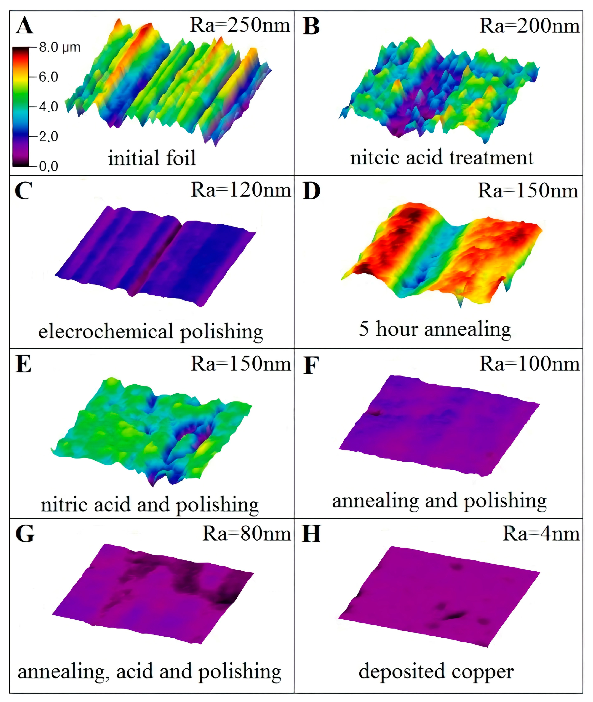
For the fabrication of a high quality and uniform graphene monolayer by CVD technology on copper foil from carbonaceous gas, it is necessary to use copper foil with the lowest value of roughness. In this work, six methods were used to form the surface with minimal roughness. The result of the analysis of surface morphology after different treatments is shown in
Figure 1.
The initial copper foil has the arithmetic average roughness R
a about 250 nm (
Figure 1A). The treatment of sample in nitric acid leads to R
a about 200 nm (
Figure 1B), while ECP can provide R
a = 120 nm of the foil (
Figure 1C). The annealing process results in the same R
a = 150 nm of copper foil as the combination of nitric acid treatment with further ECP, see
Figure 1D,E, respectively. The combination of annealing and further polishing, as well as annealing and further acid treatment and ECP results in the roughness of 100 and 80 nm and is presented in
Figure 1F,G, respectively. For comparison, the morphology of thin copper film (R
a = 4 nm) deposited on an optically flat single-crystal sapphire substrate is shown in
Figure 1H.
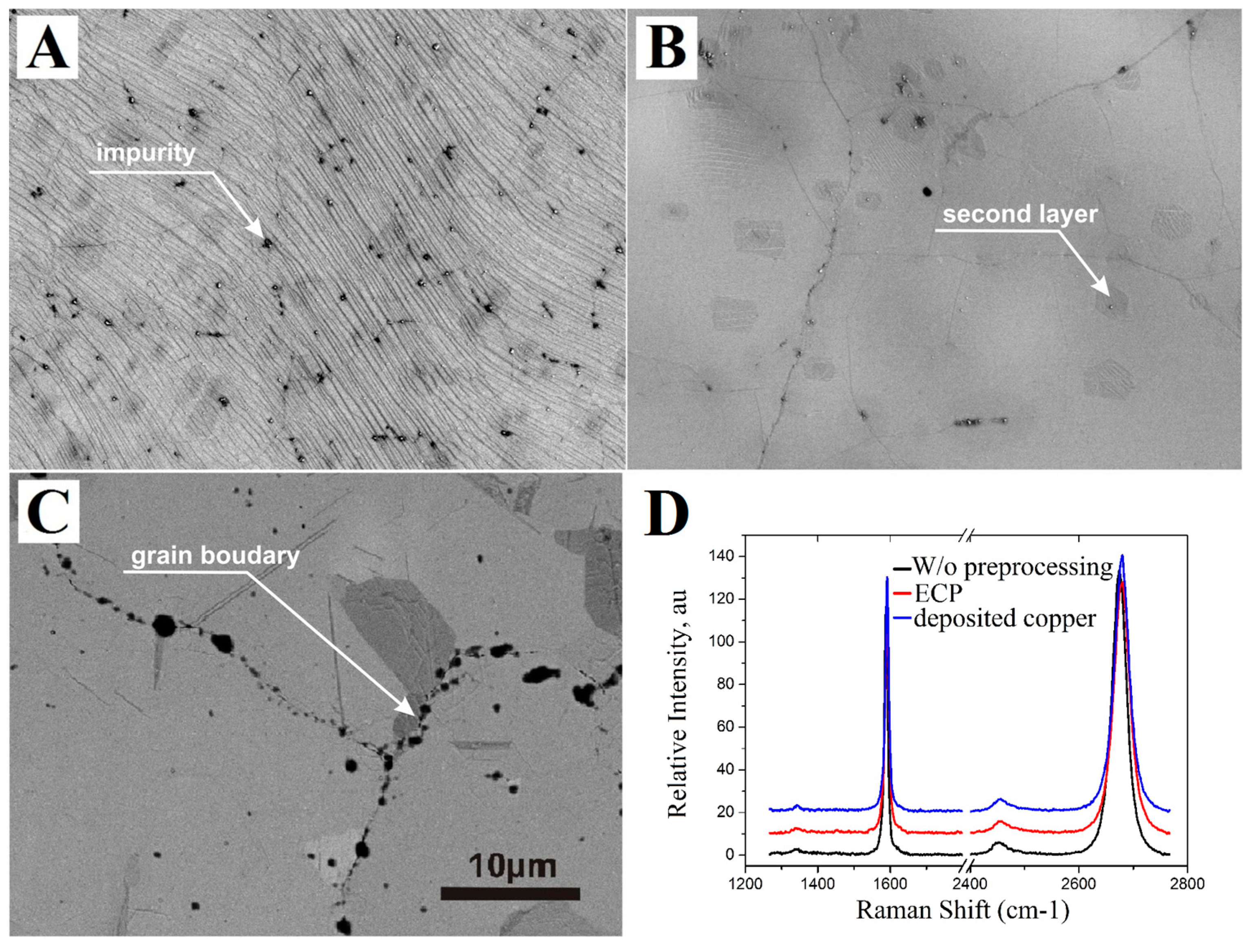
The process of nucleation of second and more layers of graphene and its correlation with defects (impurities) and the roughness of the copper surface is investigated using images obtained by electron microscope (
Figure 2). The graphene film synthesized on initial copper foils without any processing has different impurities that look like black dots in the SEM image (
Figure 2A). Almost 10% of the total area is occupied by islands of dark gray color, which correspond to double-layer graphene. The copper foil treated by a combination of annealing and ECP with synthesized graphene which has the lowest density of the few layer islands is demonstrated in
Figure 2B. Surface defects were removed by electropolishing and followed annealing of the copper surface leaded to smooth the surface more. Smoother copper surface provides lower nucleation sites for the graphene and as a result graphene film has less area of few layer. The area of the few layered graphene on the sample with the smooth deposited copper film is comparable with the area on the polished foil and combinations with it (
Figure 2C). Despite the minimal roughness of the copper film, it is not possible to completely get rid of the few layer, because it grows at the copper grain edges, unlike the irregularities and impurities in the case of copper foils. It should also be mentioned that most of the impurities on the surface of the copper film are located on the grain boundaries of neighboring crystallites.
The Raman spectra in
Figure 2D shows that the quality of graphene films is the same for all substrates and does not depend on the surface processing of copper foils, the only difference is the number and average size of islands with few layer graphene film. Measurements of the carrier mobility and sheet resistance, carried out by the four-probe method, have shown values from 2000 to 3000 cm
2/(V·s) and less than 500 Ohm/square, respectively, indicating the high quality of the synthesized graphene film.
Five regions (100 × 100 μm2) of graphene transferred onto silicon oxide were taken from each sample and analyzed using optical microscopy. With a decrease in roughness, the amount of the few layer graphene also decreases. However, with a decrease in roughness below 120 nm, the amount of the few layer graphene remains approximately the same. This can be explained by a decrease in the number of the nucleus (islands) and an increase in the size of islands with a few layer graphene film. For example, for untreated foil (Ra = 250 nm), more than 1000 islands with an area of 6–9 μm2 are obtained in the area of 100 × 100 μm2, that is, the total area of the few layer graphene film (ρ) is 6 ÷ 10% of the entire surface. After the ECP processing (Ra = 120 nm), 150–200 islands are formed in the same region, but the size of each of them is reduced to 15–20 μm2 (ρ = 2 ÷ 3%). In the case of a combination of annealing, chemical etching, and ECP (Ra = 80 nm), less than 50 islands with an area of 50 μm2 are formed on the foil, that corresponds to a percentage ρ = 2 ÷ 3%. On a deposited copper film with a roughness of only 4 nm, the formation of a few layer graphene occurs at the grain boundary of copper crystals, but the size of islands can grow significantly. So only 10–20 islands of the few layer graphene with an area of 50–100 μm2 are observed and their total area takes the same percentage ρ = 2–3%.


 ,
, 

