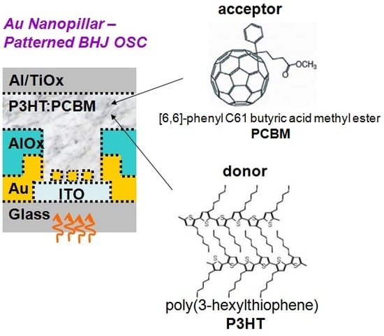
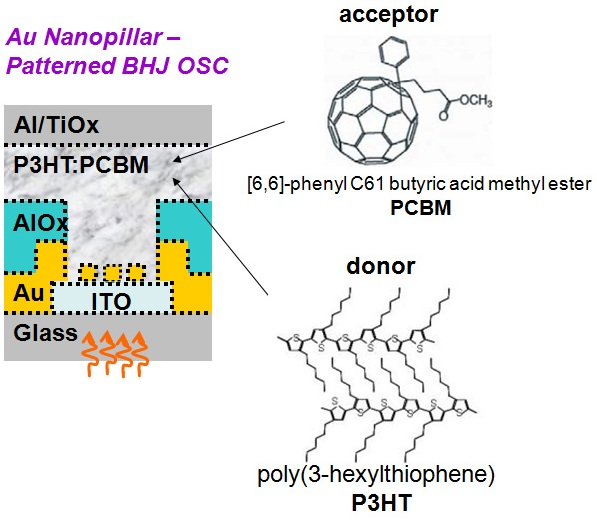
2. Results and Discussion
Our device architecture is shown in
Figure 1, and described in detail in the
Experimental Section. Briefly, Au nanopillars of varied size and spacing are patterned onto a transparent indium tin oxide electrode onto which a PCBM/P3HT mixture is deposited, followed by capping with a nonstoichiometric titanium oxide (TiO
x) layer. As will be seen below, the absence of a hole conduction layer such as PEDOT:PSS above the transparent electrode results in a relatively low overall external quantum efficiency. However the central point of this work is to investigate the effect of plasmonic resonance of noble metal particles on the efficiency of the OSCs, not to achieve an optimized design which includes such an effect. Our focus in this work is to explore the relationship between the optical extinction spectrum and external quantum efficiency of our OSC devices; we reported on the performance of similar devices under simulated solar illumination elsewhere [
13]. In this work we first carried out transmission spectrum measurements. We calculate the extinction from the measured transmission using:
where
TSample is the transmission for a given sample and
TSub is that for an ITO-coated glass substrate. As we discuss below, we observed peaks in the extinction spectra, typically identified with excitation of localized surface plasmons [
14,
15,
16].
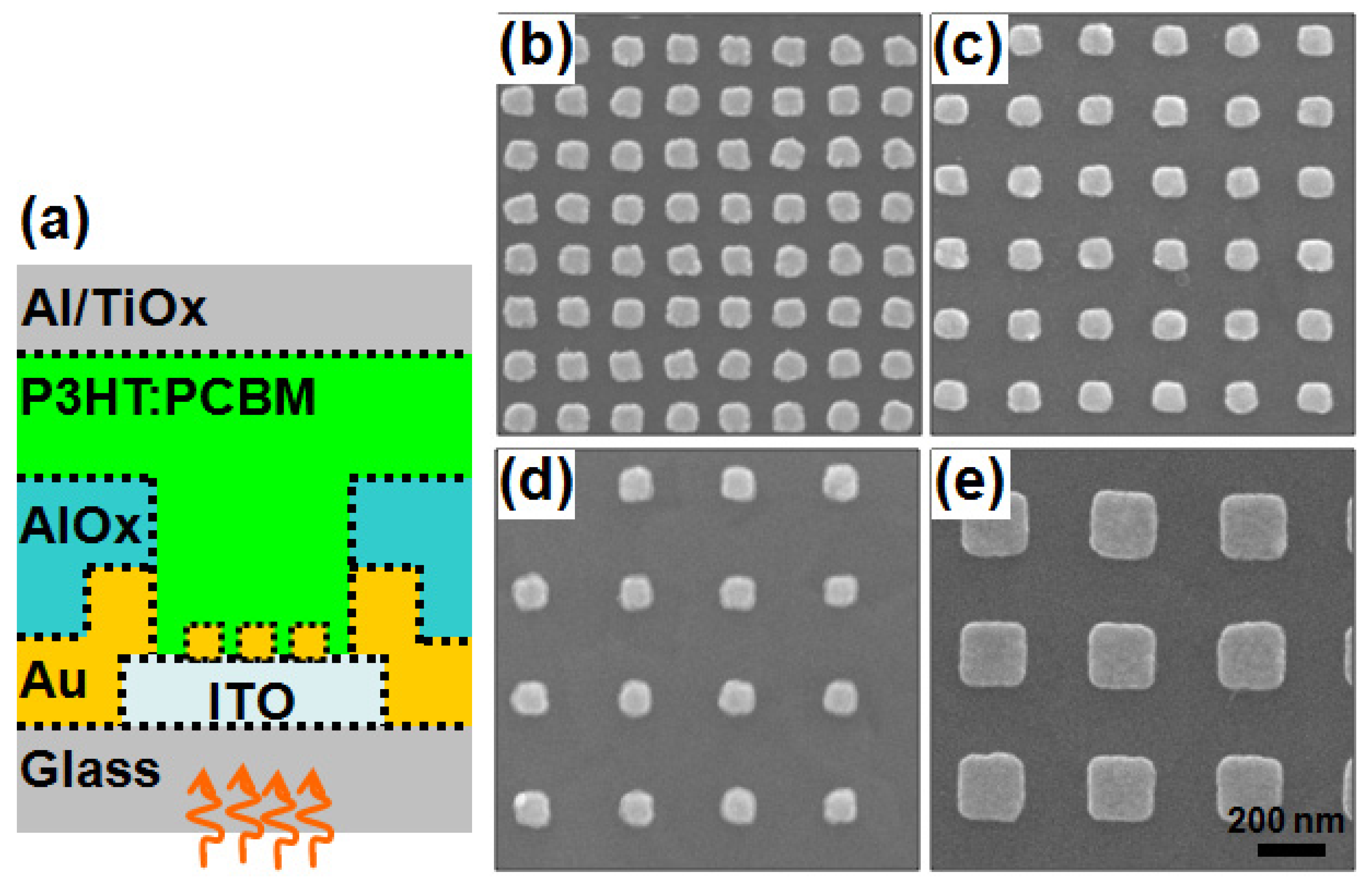
Figure 1.
(a) Schematic cross section of the NP-patterned organic solar cell design studied in this work; (b–e) SEM images of Au nanopillar arrays on ITO surface with pillars (b) 95 nm wide × 150 nm pitch; (c) 95 nm wide × 200 nm pitch; (d) 95 nm wide × 300 nm pitch; and (e) 180 nm wide × 360 nm pitch, respectively. The pillar heights are 70 nm in each case.
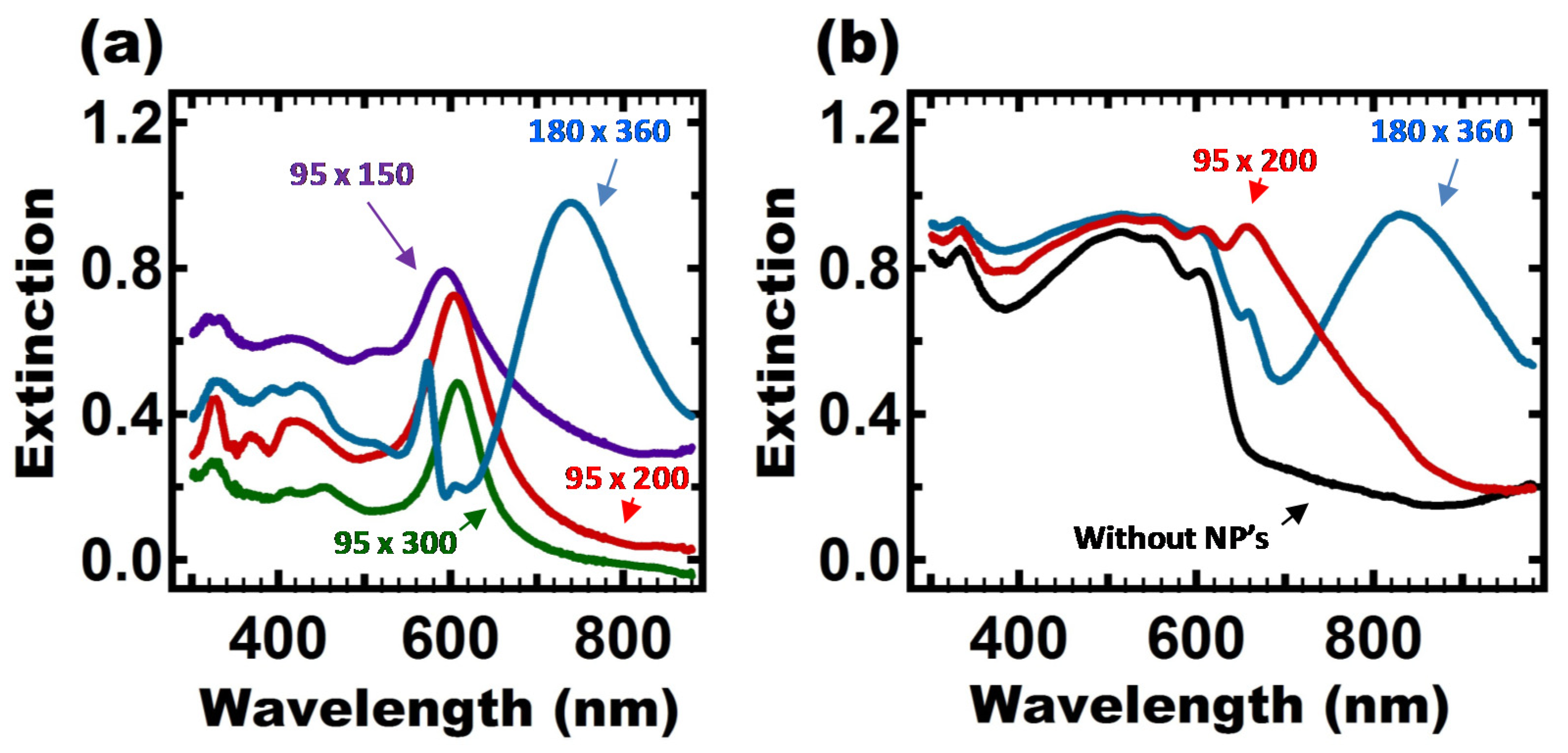
Figure 2a shows the results of transmission measurements through nanopillar arrays on ITO-coated glass substrates. For the NP array with width W = 95 nm and pitch P = 150 nm, the measured peak in the extinction occurs at 596 ± 3 nm optical wavelength (purple curve). On increasing the pitch the peak in extinction slightly shifts toward longer wavelengths, 604 ± 2 nm at a pitch of 200 nm (red curve), and 609 ± 2 nm at a pitch of 300 nm (green curve). The slight red shift in the peak in extinction with increasing pitch, can be attributed to the effect of radiative dipole coupling [
14]. For the array with W = 180 nm × P = 360 nm, the most intense peak in extinction occurs at a wavelength of 680 ± 4 nm (blue curve). This red shift in the peak in extinction as the NP width increases is consistent with the known behavior of localized surface plasmon resonances [
14,
17,
18].
Figure 2b shows the experimentally derived extinction spectra for a P3HT:PCBM film deposited on a non-NP-patterned substrate (black curve), for a P3HT:PCBM film on an Au NP array with W = 95 nm × P = 200 nm (red curve), and for a P3HT:PCBM film-coated NP array with W = 180 nm × P = 360 nm (blue curve). The thickness of the P3HT:PCBM film, as determined by profilometer measurements, was approximately 168 nm. Its presence produces a red shift in the extinction peaks, consistent with the increase in dielectric constant of the medium surrounding the nanopillars [
14]. The measured red shifts are from approximately 604 nm to 657 nm for NP arrays with W = 95 nm × P = 200 nm, and from 680 nm to 830 nm for NP arrays with W = 180 nm × P = 360 nm.
Figure 2b also shows a second, less intense NP-associated peak in the extinction spectrum for the W = 180 nm × P = 360 nm arrays near λ = 660 nm, apparently due to a higher-order particle plasmon mode; it is red shifted from λ ~ 560 nm for the bare NP array, and less intense than the peak for the W = 95 nm arrays. The peak in extinction for P3HT:PCBM-coated NP arrays with W = 95 nm × P = 150 nm occurs at approximately 650 nm (curve not shown). We did not measure the extinction spectrum for P3HT:PCBM-coated nanopillar arrays with W = 95 nm × P = 300 nm, but extrapolating the red shift based upon that for samples with pitch 150 nm and 200 nm, would give a peak at approximately 664 nm.
The results presented above are consistent with an increase in the optical extinction due to excitation of particle plasmons in our NP array-containing OSC devices. We next examine whether this results in an associated broadening in the absorption spectrum of the P3HT:PCBM layer, and in the EQE spectrum of OSC devices.
Figure 2.
(a) Extinction spectra from NP-patterned arrays on ITO-coated glass substrates with 95 nm wide × 150 nm pitch pillars (purple curve), with 95 nm wide × 200 nm pitch pillars (red curve), with 95 nm wide × 300 nm pitch pillars (green curve), and with 180 nm wide × 360 nm pitch pillars (blue curve); (b) Corresponding extinction spectra after coating with a 168 nm thick layer of P3HT:PCBM. The red curve is for NP arrays with W = 95 nm wide × P = 200 nm, the blue curve is for that with W = 180 nm × P = 360 nm, and the black curve is for P3HT:PCBM on ITO- coated glass substrate.
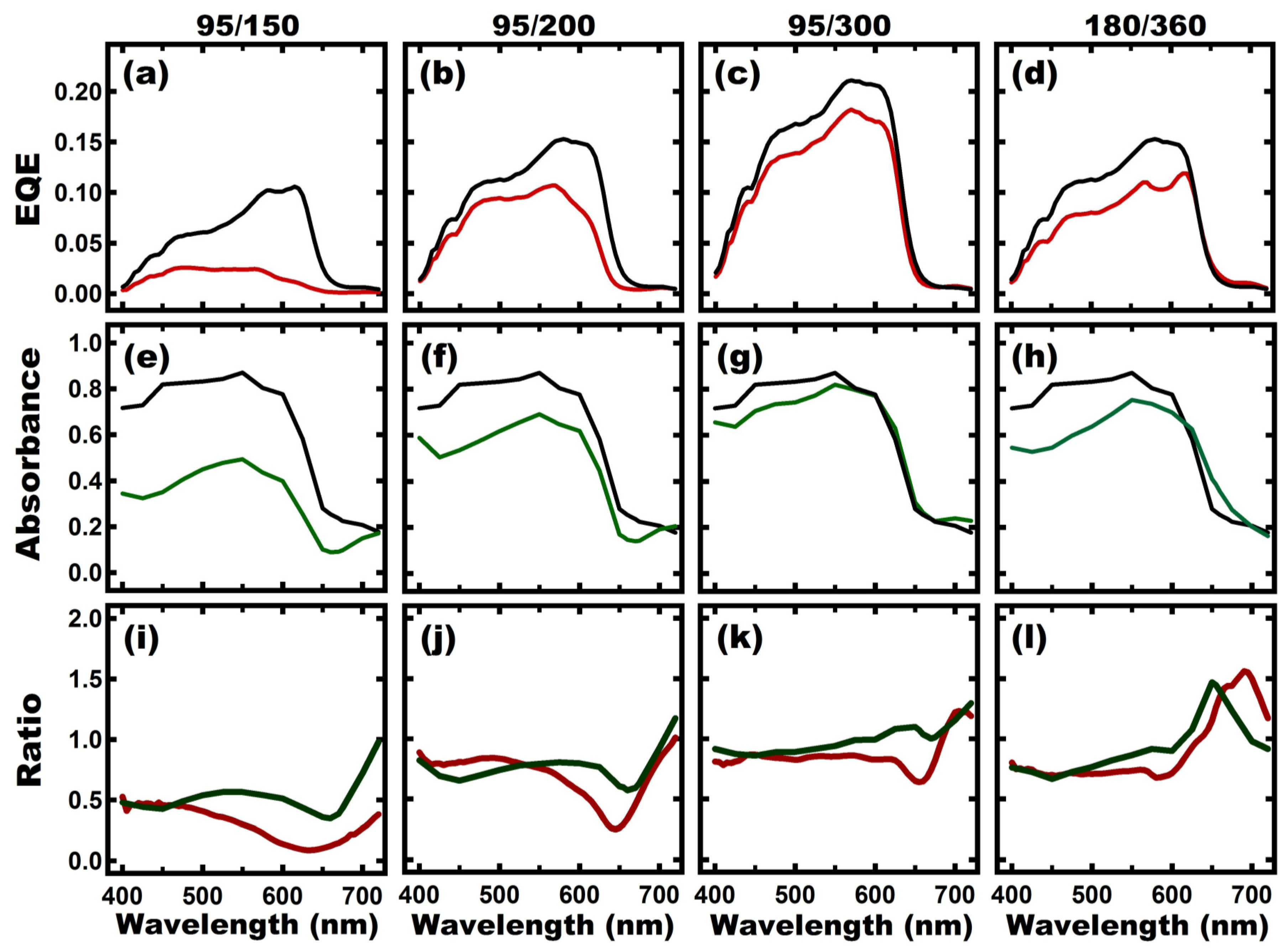
Measured external quantum efficiency (EQE) spectra for devices with (red curves) and without (black curves) arrays of NPs are shown in in
Figure 3a,d. The differences in the overall level of the EQE spectra for cells without NP’s we attribute to variation in the phase separated domain structure within the active layer, which is sensitive to the details of the deposition and annealing; an advantage of our sample design is that it allows a direct comparison of the EQE between cells with and without NP’s on the same substrate so that the effects of such differences are minimized. The pillar widths and pitches for these spectra are (a) W = 95 nm × P = 150 nm, (b) W = 95 nm × P = 200 nm; (c) W = 95 nm × P = 300 nm, and (d) W = 180 nm × P = 360 nm. Comparison of the NP array and control spectra in
Figure 3a–c shows that for the W = 95 nm arrays there is no enhancement in the EQE at the wavelengths where we observe peaks in the extinction spectra (
i.e., 650 nm, 657 nm, and 664 nm, respectively). The NP-associated peaks in extinction for the smaller, 95 nm width nanopillars do not give rise to enhanced solar cell efficiency. Instead they show a decrease in EQE near the optical wavelengths corresponding to NP-associated peaks in the extinction. In contrast, for the wider, W = 180 nm pillars (red curve in
Figure 3d) a slight increase in the EQE is observed in the wavelength range from approximately 640 nm ~ 720 nm, bracketing the less intense peak in the extinction spectrum.
To understand the lack of simple correspondence between NP-associated peaks in the optical extinction and the measured EQE spectra for the W = 95 nm NP arrays, we calculate the absorbance within the P3HT:PCBM layer. Our previous results demonstrated that the calculated organic layer-absorbance is in good semi-quantitative agreement with the measured EQE of a NP array-patterned OSC [
13]. The details of the calculation were discussed previously [
13]. Based upon the observed corner rounding in our SEM images we approximated the W = 95 nm pillars as cylindrical, but used square cross sections for larger W = 180 nm pillars.
Figure 3e–h show calculated absorbance spectra, corresponding to the measured EQE spectra for the devices of
Figure 3a–d. The agreement is good between the calculated absorbance and measured EQE, both for the devices with (green curves in
Figure 3e–g) and without (black curve; reproduced in each of
Figure 3e–g for ease of direct comparison). We note that there is considerable rounding of the corners of the 95 nm wide Au pillars. We investigated the effect that this might have by comparing the calculated absorption for the square cross section pillars with the extreme case of cylindrical pillars. As shown in the
supplementary material (Figure S1) this produces only very minor changes in the calculated spectrum, so that the agreement with the measured EQE remains good. The overall EQE for the device without nanopillar arrays is larger, in particular at wavelengths less than approximately 620 nm. We find that the reduction in both EQE and in calculated absorbance in this region increases monotonically with the area fraction covered by Au nanopillars, indicating that it is mainly due to the limited light transmitted through the arrays into the active layer. Consistent with the measured EQE spectra, the calculated P3HT:PCBM absorbance spectra for the NP-patterned devices with W = 95 nm (
Figure 3e–g) are lower than that for the control device in the spectral region corresponding to the peaks in extinction. For the NP-patterned device with W = 180 nm, the absorbance is enhanced in the region from approximately from 620 nm to 700 nm, again qualitatively consistent with what we observe in the measured EQE spectra. Our earlier calculations indicated that this enhancement is associated with interference and diffraction effects due to presence of Au nanopillar arrays [
13]. To make a more detailed comparison, we calculated the ratios of both the EQE and absorption spectra, with and without NP arrays as a function of pillar width and pitch. The ratio curves for the absorbance (green curves) and EQE (red curves), shown in
Figure 3i–k, are similar in shape; both show dips near 650 nm, with a slight blue shift in that of the EQE relative to that in the absorbance, and with an overall red shift as the pitch of the array is increased. These dips are seemingly associated with the measured peaks in optical extinction,
i.e., that peaks in extinction correspond to dips in the EQE, at least for the smaller 95 nm width NP’s we investigated. This result is qualitatively consistent with Morfa’s [
5] findings but conflicts with Lee’s [
6] report of an increase in measured EQE at the peak wavelength in the extinction spectrum for a device containing Au nanoparticles.
Figure 3.
(a–d) Measured EQE for OSC devices with Au nanopillar arrays (red curves) and without (black curves); (e–h) Calculated P3HT:PCBM absorbance for devices with Au nanopillar arrays (green curves) and without (black curves); (i–l) Red curves are for ratios of measured EQE for devices with Au NP arrays and without and green curves are for ratios of calculated absorbance for devices with Au NP arrays and without. Panels from left to right are for Au NP-patterned cells with W = 95 nm × P = 150 nm, W = 95 nm × P = 200 nm, W = 95 nm × P = 300 nm, and W = 180 nm × P = 360 nm.
To reiterate, the motivation for the incorporation of noble metal nanoparticles in OSC devices is to enhance the optical absorbance in the organic active layer due to field enhancement associated with the particle plasmonic response to incident light. To return for a moment to the issue of the absence of the PEDOT:PSS layer in our devices, we note that some effect on the localized surface plasmon might be expected based on the change of the dielectric environment of the noble metal nanoparticles due the presence of this layer. However, since the typical thickness of the PEDOT:PSS layer (>70 nm) used for OSCs would place the active layer materials well beyond the range of the plasmonic evanescent field from the noble metal particles; we thus expect that the enhancement of the absorption would be even smaller if such a layer were present.
It is also interesting to note that for simpler geometries, the maximum field enhancement usually coincides with the peak in extinction [
14], and thus with the expected enhancement in the EQE of an OSC device. This however is the opposite of what we have seen in the correspondence between our extinction measurements and the EQE measurement; it leads us to ask whether field enhancement within the organic layer does occur at wavelengths corresponding to particle plasmon excitation in our devices. Fluorescence maps of molecular films on metallic nanostructures have been demonstrated to reveal the excitation of particle plasmon and surface plasmon resonances in such structures [
17,
18,
19,
20,
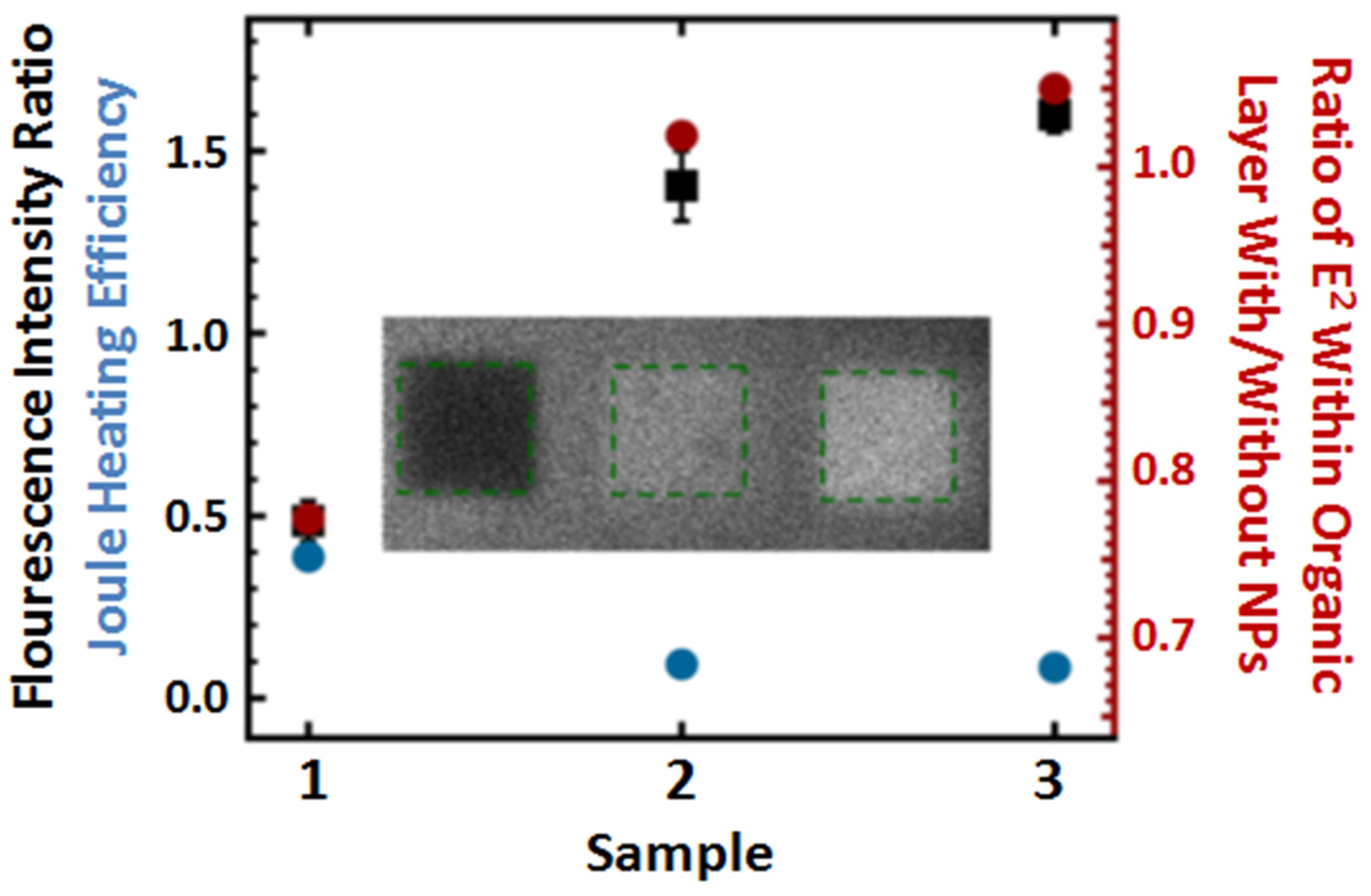
21]; locations in the map where enhancement in fluorescence occurs indicate regions of localized field enhancement. The insert in
Figure 4 shows a fluorescence map across three different P3HT:PCBM film-covered NP arrays on an ITO coated glass substrate (for this measurement no Al/TiOx layers were deposited).
Figure 4.
(insert) Fluorescence map across three different P3HT:PCBM film-covered NP arrays #1 to #3 indicated by the green dashed squares for W = 95 nm × P = 180 nm (left square), W = 95 nm × P = 300 nm (center square), and W = 180 nm × P = 360 nm (right square). The image was measured with a scanning laser microscope using a 633 nm wavelength source, collecting fluorescence at wavelengths above 660 nm. The black solid squares show the ratio of the fluorescent intensity from the corresponding areas with nanopillar arrays compared to that without NP-array. The red solid circles show the corresponding ratios of calculated |E|2 integrated over the P3HT:PCBM volume not shadowed by nanopillars compared to that without NP-arrays. The blue solid circles are the corresponding calculated Joule heating efficiencies. Normal incident light from glass substrate side with 633 nm wavelength is used for the calculations.
The image was measured with a scanning laser microscope using a 633 nm wavelength source, collecting fluorescence at wavelengths above 660 nm [
17]. The visible square regions in the map are from three Au nanopillar arrays; the pillar width and pitch are (left square) W = 95 nm × P = 180 nm, (center square) W = 95 nm × P = 300 nm, and (right square) W = 180 nm × P = 360 nm. The corresponding most intense extinction peaks for these arrays occur at 654 nm, 664 nm, and 830 nm, respectively.
It is clear that the field enhancement is absent in the NP array (left square) whose extinction peak most nearly coincides the excitation wavelength! Compared to the surrounding unpatterned area, the lower intensity in this pattern instead suggests a reduction of the field strength within the organic layer. For the arrays of the center and right squares in the map the most intense peak in the measured extinction is increasingly far from the wavelength of the 633 nm excitation wavelength, yet the fluorescence intensity from the NP array increases. This trend is illustrated by black solid squares in the plot of
Figure 4, which represent the ratio between the average fluorescent intensity on the NP-patterned area to that from the un-patterned area. For the arrays with W = 95 nm × P = 300 nm (center image) and with W = 180 nm × P = 360 nm (right image) we see a slight enhancement in the fluorescence. The solid red circles in
Figure 4 show the ratio of the calculated |E|
2, integrated over the volume of P3HT:PCBM not occupied by Au nanopillars, to that calculated for the unpatterned substrate. The visual agreement between these two ratios as the width and pitch of the NP’ are changed, and the lower value of the calculated |E|
2 over the W = 95 nm × P = 180 nm NP array confirms that attenuation, rather than enhancement in field strength occurs in the active layer at peak extinction.
It has recently been suggested by Atwater and Polman [
22], that depending on their size, inclusion of noble metal particles in OSC’s may result in ohmic loss which competes with scattering of the incident light. In addition, Mie Theory predicts that for smaller particles absorption within the particles dominates scattering. We thus consider the possibility that the extra extinction in the smaller width NP arrays we have studied is dominated by nanopillar absorption, and estimate how much of the power absorbed by the nanopillars in our arrays goes to Joule heating [
23,
24,
25]. (Note that in the measured extinction spectra of
Figure 2b, the back electrode is absent; while in the calculation for Joule heating efficiency presented here it is included.) Using the complex Poynting vector theorem, the time-average Ohmic loss within an Au nanopillar [
26] can be expressed as:
where is the conductivity, is the local electrical field squared, and the integration is over the volume of a nanopillar. The relationship between the relative complex permittivity, and the complex refractive index,
, is [
27]:
where χ is the electrical susceptibility; and ε
0 is the permittivity. Thus, the conductivity can be expressed as:
Combining these expressions, the Ohmic loss within the Au nanopillars is calculated, and the Joule heating efficiency,
, is determined by dividing
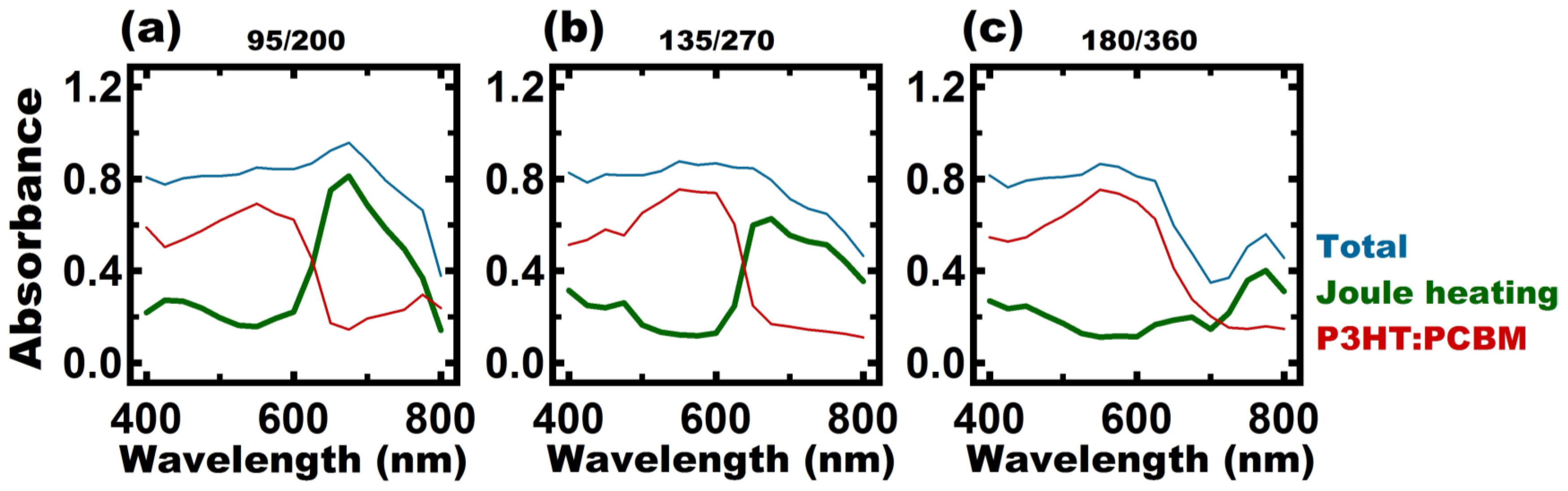
by the incident optical intensity. The green curves in
Figure 5a–c show the Joule heating efficiency for OSC devices with nanopillar arrays with (a) W = 95 nm × P = 200 nm; (b) W = 135 nm × P = 270 nm; and (c) W = 180 nm × P = 360 nm. It reaches a maximum value at a wavelength nearly coincident with the extinction peak for the smaller, W = 95 nm × P = 200 nm array. The Joule heating is also considerably smaller for the larger nanopillars in this spectral range. As the width of the nanopillar increases, the Joule heating efficiency peak red-shifts with decreasing maximum heights. The blue curves in
Figure 5 show for each device the total absorbance
, which is the sum of the calculated absorbance of the P3HT:PCBM film (red curves) and the calculated Joule heating efficiency (green curve). Compared to the extinction spectra shown in
Figure 2b, we see similar broadening in total absorbance spectra, suggesting that Joule heating contributes to the observed broadening in the extinction spectra. Especially for the case of the device with W = 95 nm × P = 200 nm pillars, the peak in the total absorbance
, appears near the measured peak in extinction, 657 nm, and is dominated by the Joule heating contribution.
Figure 5.
Calculated Joule heating efficiency (green curve), calculated P3HT:PCBM absorbance (red curve), and sum of both (blue curve) for NP-patterned devices. (a–c) for arrays with W = 95 nm × P = 200 nm, W = 135 nm × P = 270 nm, W = 180 nm × P = 360 nm, respectively. Nanopillar height is 70 nm for these arrays.
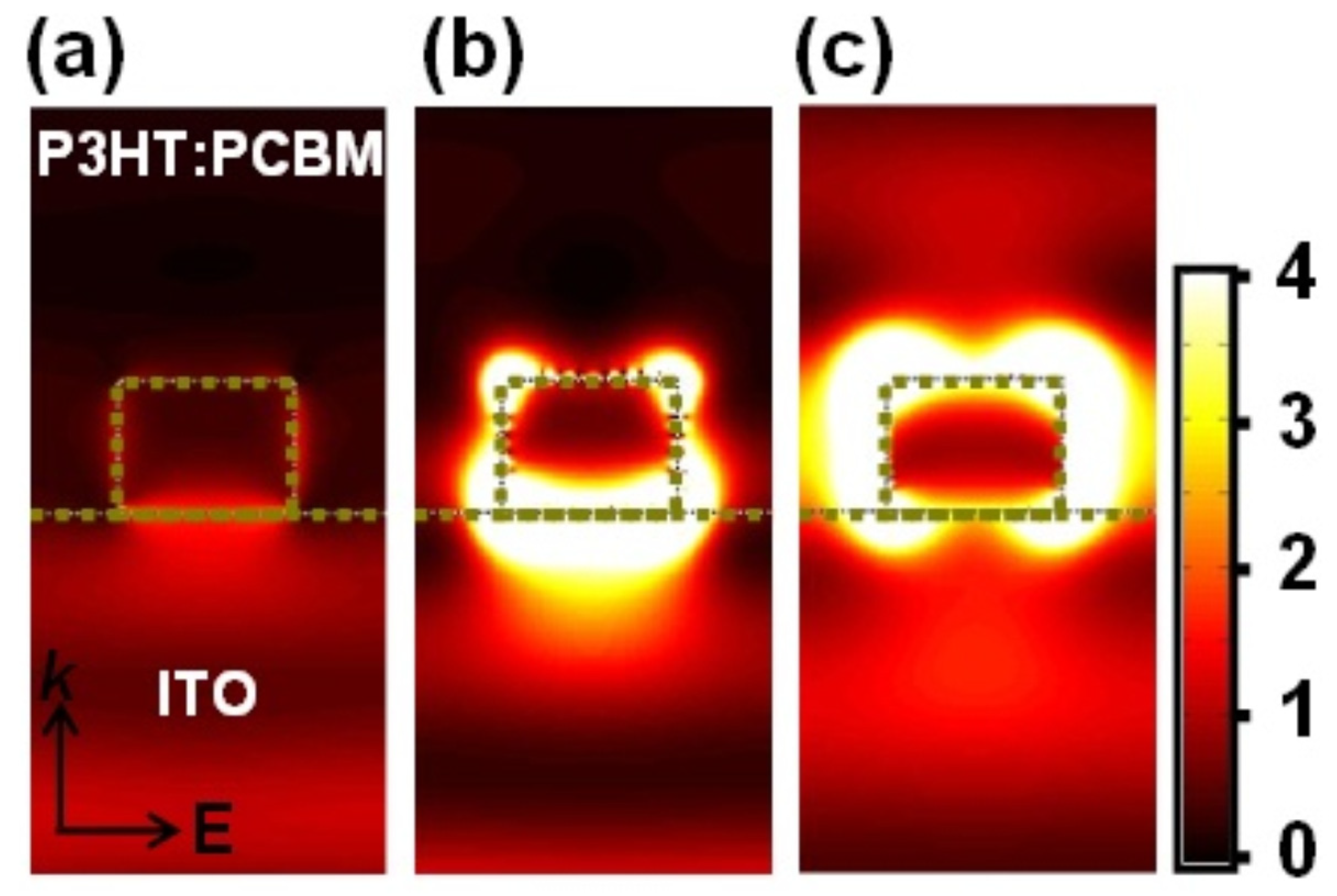
Figure 6a–c show the calculated spatial distribution of |E|
2 within a plane cutting though the center a nanopillar for an array with W = 95 nm × P = 200 nm, under normal incidence illumination at λ = 525 nm, 660 nm, and 750 nm, respectively. Near the peak in extinction (660 nm), the field within Au nanopillars is significantly more intense than that at 525 nm. Although local field enhancement is observed in close proximity to the nanopillar surface, the total field intensity integrated over the P3HT:PCBM layer is lower than that for the control device without nanopillars, consistent with the fluorescence image in
Figure 4. This indicates there is a tradeoff between the transmission and the absorption/scattering. Interestingly, for the wavelength beyond the peak in extinction,
i.e., at 750 nm, the local field enhancement near the surface gives rise to a 65% increase in the calculated organic layer absorbance; this is in qualitative, but not quantitative agreement with the slight increase in measured EQE, ~14%. The discrepancy might be due to the fact that measured photocurrent is very low beyond 720 nm wavelength, making it difficult to distinguish the difference in EQE with and without nanopillars beyond this wavelength. Our field-squared maps in
Figure 6b,c show that the enhancement is confined to a region within approximately 40 nm of the nanopillar surface. The very local nature of the intense field seemingly justifies our omitting a PEDOT:PSS interface layer (typically ~40 nm thick) in our devices.
The calculated Joule heating efficiency, shown by blue solid circles in the plot of
Figure 4 displays a nearly opposite variation with NP width and pitch as that of the measured fluorescence intensity ratio; the fluorescence thus scales with |E|
2 within the P3HT:PCBM film, but not within the Au nanopillars.
Figure 6.
(a–c) Cross sectional |E|2 maps, cutting though the center of the nanopillar for devices with NP-patterned arrays with W = 95 nm × P = 200 nm, and height = 70 nm. The incident optical wavelengths from left to right are 525 nm, 660 nm, and 750 nm.
Figure 6.
(a–c) Cross sectional |E|2 maps, cutting though the center of the nanopillar for devices with NP-patterned arrays with W = 95 nm × P = 200 nm, and height = 70 nm. The incident optical wavelengths from left to right are 525 nm, 660 nm, and 750 nm.


