A Universal Design of FPGA-Based Real-Time Simulator for Active Distribution Networks Based on Reconfigurable Computing


1
Key Laboratory of Smart Grid of Ministry of Education, Tianjin University, Tianjin 300072, China
2
State Grid Economic and Technological Research Institute Co. Ltd., Beijing 102209, China
*
Author to whom correspondence should be addressed.
Energies 2019, 12(11), 2086; https://doi.org/10.3390/en12112086
Submission received: 23 April 2019
/
Revised: 24 May 2019
/
Accepted: 28 May 2019
/
Published: 31 May 2019
(This article belongs to the Section F: Electrical Engineering)
Abstract
:Reconfigurable computing is that the logical resources in the system can be reconfigured according to the real-time changing data flow to achieve different calculation functions. The reconfigurable computing system has both high efficiency on hardware and universality of software. The field programmable gate array (FPGA)-based real-time simulator for active distribution networks (ADNs) requires a long compilation time for case modification, with low efficiency and low versatility, making it inconvenient and difficult for users. To solve the problem of long compile time with a new case, a universal design of the FPGA-based real-time simulator for ADNs based on reconfigurable computing is proposed in this paper. It includes the universal design of the simulation parameter configuration, the simulation initial value setting, the linear equations solving module and the simulation result output module. The proposed universal design of the simulator makes the modification and change of the cases and parameters without recompiling and further improves the simulation efficiency. Simulation results are conducted and compared with PSCAD/EMTDC to validate the correctness and effectiveness of the universal design.
1. Introduction
In recent years, with fast development and maturity of distributed generators (DGs) and microgrids [1], the structures and operation modes of distribution networks are undergoing tremendous changes [2]. Gradually, traditional distribution networks are transformed into active distribution networks (ADNs) [3]. The dynamic characteristics of ADNs are complicated, due to the integration of new devices and the application of new technologies [4]. Thus, researchers prefer to use transient simulation tools with detailed models to explore the dynamic characteristics and operation mechanisms of ADNs [5]. Compared with off-line transient simulation [6], real-time simulation of ADNs can not only simulate the complex dynamic and static characteristics of various equipment components within the system, but also perform hardware-in-the-loop (HIL) simulation with external physical devices. HIL simulation is of significance in online tests of hardware devices, such as the control and protection devices of ADNs [7].
At present, commercial real-time simulators, mainly represented by RTDS (real time digital simulator) [8], eMEGAsim [9], HYPERSIM [10] and NETOMAC [11], have been widely applied in various fields of power systems. Application scenarios include system stability research [12,13], relay protection device test [14,15], FACTS (flexible alternative current transmission systems) controller design [16] etc. Traditional real-time simulators are mainly used in the studies of transmission grids. Compared with transmission grids, ADNs have higher requirements on the computing capability of real-time simulators, due to the diverse types of DG, the complex controller function, and the high switching frequency of power electronic device. The aforementioned real-time simulators adopt latency-oriented hardware resources, such as central processing units (CPUs) and digital signal processors (DSPs), and can improve the computing capacity only by multi-processor parallel mode. However, due to the heavy burden of communication, it is difficult to guarantee real-time performance. Therefore, it is difficult to fully meet the computing needs of large-scale real-time simulation of ADNs.
Field programmable gate array (FPGA) has advantages on the highly parallel hardware structure, the pipeline processing architecture and the programmable characteristics, making it suitable for the real-time simulation of power systems. In terms of joint simulation with other devices, Reference [17] realizes the joint real-time simulation of RTDS, FPGA and TSA (transient stability analysis), in which FPGA is only used as a high-speed communication tool, and the computational capacity of FPGA is not fully utilized. In References [18,19], FPGA is used to simulate specific elements, such as power electronic converters and motors. References [20,21] realize the co-simulation of FPGA and an industrial control machine, in which FPGA is used as the solver. With the decreasing of manufacturing cost and the maturity of FPGA, real-time simulation fully realized with the FPGA has received more attention. Reference [22] adopts a development board integrated with multiple FPGAs to implement a real-time simulation of large-scale power systems. Reference [23] implements a real-time simulation of power electronic systems and applies to controller hardware-in-the-loop testing. Reference [24] proposes the real-time simulation method for the control system and the interaction of electrical and control system. Reference [25] studies the synchronization mechanism and interface design of the multi-FPGA real-time simulator for ADNs, and realizes the communication and co-simulation of the multi-FPGA development board.
Although FPGA has the advantages of high computing speed and programmable structure, it takes as long as hours to compile when a case has been modeled or modified. The compilation process, including analysis and synthesis, placing and routing, and timing analysis, is a complicated optimization process that translates high-level hardware description language (HDL) into individual bits and wires. For larger FPGA design, the compilation process may take hours or even days [26]. The mentioned long compilation time is required to achieve optimal utilization of FPGA resources. It is possible to shorten the compilation time with techniques, e.g., from References [26,27]. However, it is at the cost of inferior design with larger critical path delays, which is detrimental for the performance. As FPGA device capacity grows, the compilation time will also increase [27]. Although the computing capabilities are improving, the problem of compilation time will not be fundamentally solved.
For the FPGA-based real-time simulator for ADNs, the compilation time is also the bottleneck that restricts the simulation efficiency and application promotion. Because the design of the FPGA needs to be modified and recompiled when the parameters are modified or a new case is to be simulated, it is with extremely low efficiency for users to use. In addition, compilation needs to be done in the EDA (electronic design automation) tools of FPGA. In the current practice, users need to operate the EDA tool of FPGA to compile and download every time the simulation case is modified, as reported in both [28] and [29]. Even though the compilation time can be shortened, it is not friendly for the users working in the field of power systems with minimal knowledge of FPGA. Previous studies have paid little attention to this problem and seldom considered the impact of the time-consuming compilation process on the application efficiency of FPGA-based real-time simulators.
Some research has been carried out on the universal design of power system simulation. Reference [30] develops a general dynamic model of wind turbines, and Reference [31] proposes a universal photovoltaic (PV) power generation system model. The above research on the universal design mainly focuses on the universality of modeling to solve the compatibility and adaptability problems of the models. In serial-based simulation programs, it will not face the problem of long compilation time after the modification in the design. Moreover, it is difficult to realize the universal design of the FPGA-based real-time simulator by simply transplanting the method to the serial programs because of the parallel structure and design. Therefore, it is necessary to study the universal design method of the FPGA-based real-time simulator from the perspective of hardware design.
In the 1960s, Gerald Estrin first put forward the concept of reconfigurable computing [32], which has both high efficiency of hardware and programmability of software. With the progress of hardware technology, reconfigurable computing has become a research hotspot, and is gradually put into practical application in the field of high-performance computing. Its recognized definition was proposed in 1999 [33]. Due to different application fields, how to design a corresponding universal structure based on reconfigurable computing for a specific application domain is a crucial issue.
In this paper, in order to solve the problem of a time-consuming compilation process in the FPGA-based real-time simulator, and to fully consider the hardware architecture of FPGAs and algorithmic process of transient simulation, universal design of the FPGA-based real-time simulator is proposed based on the idea of reconfigurable computing. The simulator using the proposed universal design does not need to be recompiled when modifying cases, completely eliminating the time-consuming and inconvenient compilation process in the EDA tools. The efficiency of simulation calculation is greatly improved, and for users, the simulator can be used friendly without having to learn how to use the EDA tools of FPGA.
The rest of this paper is organized as follows. In Section 2, the idea of reconfigurable computing is introduced briefly, and the architecture of the FPGA-based real-time simulator is presented based on reconfigurable computing. From the aspects of limiting versatility, Section 3 puts forward the detailed universal design to the related module to make the simulator have the capabilities of reconfigurable computing. Several cases are simulated and validated in Section 4, and by comparing with the simulation results of the commercial software PSCAD/EMTDC [34], the correctness and the effectiveness of the universal design proposed in this paper are fully verified. Conclusions are presented in Section 5.
2. Overall Architecture of the FPGA-Based Real-Time Simulator Based on Reconfigurable Computing
2.1. Reconfigurable Computing
The typical structure of a reconfigurable computing system includes reconfigurable computing parts, operation control parts and software environment. Reconfigurable computing parts are responsible for data calculation, and these parts are reconfigurable and can realize different functions through programming. The operation control parts are responsible for the system control, which is used for programming the reconfigurable computing parts. The software environment is responsible for data management and scheduling [35]. Moreover, the obvious feature of most reconfigurable computing systems is that the control flow is effectively separated from the data flow, the control flow is used to change the function of the reconfigurable computing part, and the data flow is transmitted to the reconfigurable computing part for calculation.
The operation of a reconfigurable computing system is divided into two phases: Configuration and execution [36]. Under the control of the main processor, the configuration control flow is transmitted to the reconfigurable hardware operation part, which is used to determine the actual operation mode of the hardware. The configuration phase is loaded at program startup, and after the configuration phase, the execution phase begins.
The implementation of computing functions can be regarded as a two-dimensional structure composed of time and space. Compared with the hardware special circuit in which the time dimension and space dimension are both invariable and the general processor in which only the time dimension is variable, the reconfigurable computing system realizes the programmability of time and space dimensions, and can change the computing solution time and enable each part of the module to participate in the calculation according to different requirements.
2.2. Architecture Design of the FPGA-Based Real-Time Simulator Based on Reconfigurable Computing
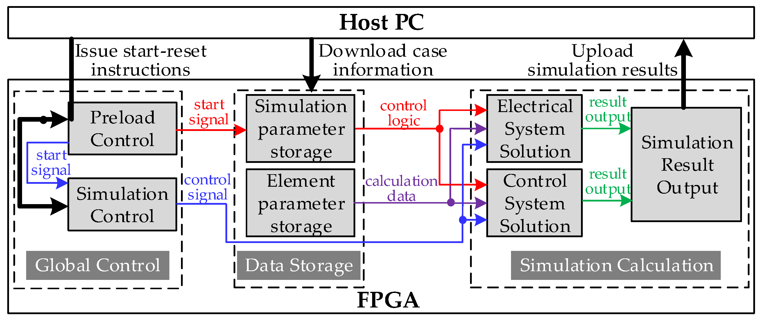
Considering the requirements on the universal FPGA-based real-time simulator and the idea of reconfigurable computing, the structure of the simulator is proposed, as shown in Figure 1.
The FPGA-based real-time simulator for ADNs is mainly divided into the off-line processing part located in the host PC and the real-time simulation part located in the FPGA. The host PC is mainly responsible for reading and topology recognition of simulation cases, as well as storing and displaying simulation results. The FPGA part is mainly responsible for real-time simulation solution of ADNs, including electrical system solving and control system solving [24].
The universal design proposed in this paper is a further development and improvement of the FPGA-based real-time simulator for ADNs [37], and the basic methods of transient simulation calculation are from Reference [37]. Reference [37] mainly considered the algorithm and parallelism of implementing transient simulation calculation in FPGA, and this paper aims to design the overall structure of the simulator so that the simulator is with the ability of reconfigurable computing. Usually, the hardware design of the FPGA-based real-time simulator needs to be modified according to the changes in the simulation cases. Although it has a higher efficiency of hardware calculation, it is not universal. In order to realize the reconfigurable computing of the simulator, this paper considers separating the part that needs to be changed with the simulation cases and the part that is independent of the simulation cases. The real-time simulation part located in the FPGA can be divided into three parts: Global Control, Data Storage and Simulation Calculation, as shown in Figure 1.
- Global Control is mainly used to control the simulator operation.
- Data Storage is mainly used to store the parameters of the simulation case, including simulation parameters, such as simulation time-step and numbers of the elements, and element parameters, such as equivalent conductance and element node number.
- Simulation Calculation is mainly responsible for the operation and processing of the calculation. The calculation processing logic is irrelevant with the case to be simulated, but can be controlled and reconfigured by simulation parameters.
- In addition, the host PC, as a software environment, is responsible for scheduling FPGA start and reset, and is responsible for managing and downloading case data.
In order to reconfigure Simulation Calculation, the preload process is set before the simulation. In the preload process, the simulation parameters, as the control flow, are read to Simulation Calculation to configure its logic. It includes three aspects: (a) enabling different modules to participate in the calculation according to the types of elements to be simulated; (b) controlling the pipeline length of the element modules according to the numbers of the elements to be simulated; (c) controlling the number of clock cycles required for each step calculation according to the solution time step set by users. The element parameters, as the data stream, are read directly from the memories to participate in the simulation calculation.
For Data Storage, in order to avoid the timing error and fan out problems that may be caused by the long-distance transmission of data signals across multi-layer modules, this paper adopts the form of distributed storage. In each element module, several memories are set to store the parameters of this type of element, and the parameters are read out to participate in the real-time simulation calculation in their own element module.
The universal real-time simulator, based on the idea of reconfigurable computing, has both advantages on the efficiency of hardware and the programmability of software. It should be noted that the reconfigurable computing implemented in this paper does not rewire the FPGA chip with the cache logic inherent in the dynamic reconfigurable FPGA itself. This paper is aimed at solving the problem of the time-consuming compilation process affecting simulation efficiency and proposes a universal design. Using the idea of reconfigurable computing, a new design of the structure of the FPGA-based real-time simulator is proposed, and according to the case to be simulated, Global Control realizes different control logic. Therefore, the simulator has the performance of high-speed real-time simulation and the universality of modifying cases online without recompiling. The dynamic reconfiguration of FPGA is mainly used to solve the resource issue and achieve more functions with limited FPGA resources. In the future work, we will consider the application of dynamic reconfiguration in the development of the FPGA-based real-time simulator, so that a larger scale power system can be simulated in a single FPGA.
3. Detailed Implementation of the Universal Design of the FPGA-Based Real-Time Simulator
In this section, the detailed implementation of universal design is carried out for the modules that follow the universality. Then Simulation Calculation can be reconfigured by the control flow of Global Control and Data Storage, and Simulation Calculation does not need to be changed with the case to be simulated. It mainly includes the following four aspects.
- Before the start of the simulation, according to the simulation parameters as the control flow, the relevant operation control logic in Simulation Calculation is reconfigured so that different cases can be calculated in this part.
- Before the start of the simulation, the initial values of the simulation calculation are set so that the initialization of Simulation Calculation is completed.
- The linear equations solving module in Simulation Calculation is designed so that it is compatible with equations of different dimensions without changing with the simulation case.
- The simulation result output module in Simulation Calculation is designed so that the output results can be adaptive to change with the user’s choice as the control flow.
3.1. Universal Design of the Simulation Parameter Configuration
As mentioned above, the preload process is set before the simulation calculation begins. The simulation parameters in Data Storage are read, and the relevant operation control logic in Simulation Calculation is reconfigured according to the parameters. Then, the reconfigurable computing of Simulation Calculation is realized.
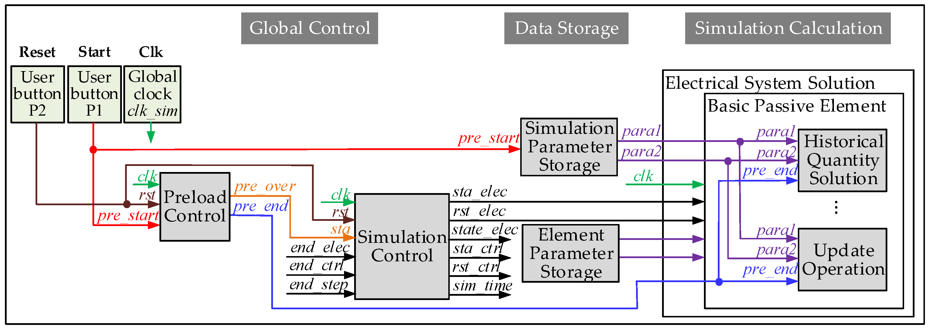
The preload process is illustrated with the basic passive element (RLC element) module in the electrical system solution module as an example. The design of the electrical system parameter information configuration is shown in Figure 2. All the clock signals in the figure are connected to the global clock clk_sim, which will not be marked for the sake of simplicity.
To achieve the above functions, the preload control module is set. According to levels of the three signals of this module, the preload process includes the following three stages:
- The signal pre_start is set to the high level: The parameter reading start signal pre_start is entered by the user button to start the preload process. At the same time, the signal is transmitted to the simulation parameter storage module. The reading of parameters is controlled by the finite state machine. When the high level of pre_start is detected, the finite state machine operates. At each state, one parameter is read out from the memory and assigned to the corresponding register. Then, the parameter is transmitted to the relevant module through the port.
- The signal pre_end is set to the high level: After tpre1 time, the simulation parameter reading has been completed, and the parameter configuration start signal pre_end is set to the high level. The signal is transmitted into sub-modules of the element modules (such as the historical quantity solution module in the basic passive element module). When the high level of pre_end is detected, the input simulation parameter data signals are assigned to the corresponding register.
- The signal pre_over is set to the high level: After tpre2 time, the simulation parameter configuration has been completed, and the real-time simulation start signal pre_over is set to the high level. The signal is transmitted to the simulation control module, and the simulation control module begins to generate the control signals of each time step periodically according to the simulation time step. At this point, the preload process has been completed.
The two time intervals, tpre1 and tpre2, are present in the FPGA design. The value of tpre1 depends on the number of simulation parameters to be read, with an appropriate margin. The value of tpre2 needs only to be sufficient to complete the read and write operations of transmitting to the submodules, and they don’t need to be changed with different cases.
For the basic passive elements, there are three simulation parameters, namely, the state containing basic passive elements (represented by a binary number, if yes, it is “1”, otherwise “0”), the number of basic passive elements and the number of nodes of basic passive elements. The first parameter determines whether the basic passive element module in Simulation Calculation is enabled and can participate in the calculation, and the last two parameters are used to control the pipeline length of the basic passive element solution. The same is true for other elements.
In this way, the online programming reconfiguration of Simulation Calculation is implemented through the control flow of Global Control and Data Storage.
3.2. Universal Design of the Simulation Initial Value Setting
In order to make Simulation Calculation reconfigurable, it is necessary to initialize it before simulation calculation so that the calculation is not affected by the previous simulation results.
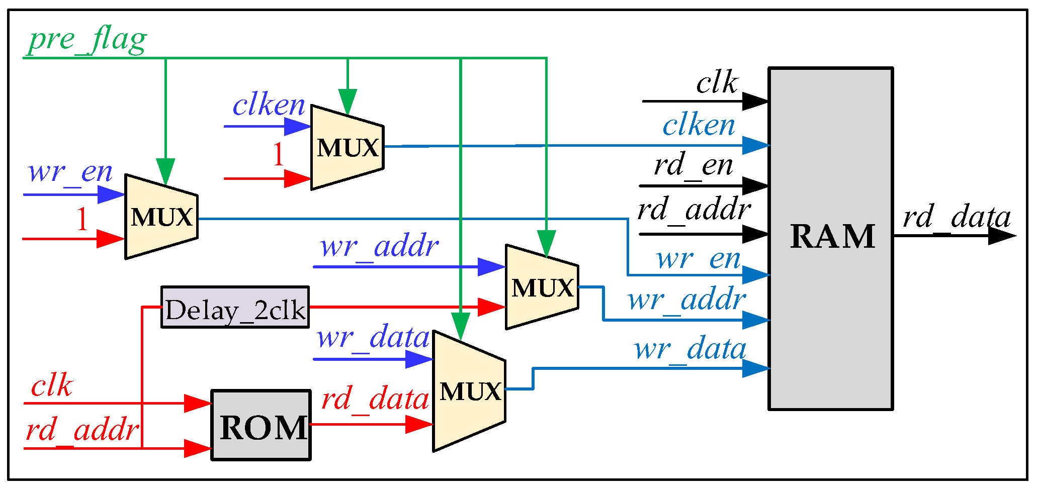
In the running process of the real-time simulator, a large number of RAMs (random-access memory) are needed to store the intermediate simulation results so that these results can participate in the simulation calculation of the next time-step. The global reset button of the FPGA will reset the registers but not the data stored in RAMs. The calculation results of the element modules are stored in RAMs, which will result in the calculation initial values of the latter case are actually the calculation results at the last moment of the previous simulation, so the values in RAMs must be reset.
The implementation method of simulation initial value setting is to set a ROM (read-only memory) corresponding to each RAM that needs to be set as initial values. During the preload process, the initial values stored in the ROM are read out and written to the corresponding RAM. Initial values are mainly divided into two categories: One is the initial values of transient numerical calculation, and the other is the element parameters related to the calculation case. The former, such as the initial values of the voltages and currents of the basic passive elements, are generally set to 0 of the corresponding numbers (consistent with the numbers of the elements). The latter, such as the amplitudes and initial phases of the source elements, can be set to the initial values of the relevant parameters of a new case.
The design of the simulation initial value setting is shown in Figure 3. The main process of the simulation initial value setting is to connect the write address signal wr_addr and the write data signal wr_data of the RAM with the read address signal rd_addr and the read data signal rd_data of the ROM respectively. The initial value setting process is also controlled by the finite state machine. Since the read data signal of the ROM has a delay of 2 clocks relative to the read address signal, a delay module is set between the write address signal of the RAM and the read address signal of the ROM to delay 2 clocks as well, so that the data stored at the same address in the ROM and the RAM are consistent. Considering that the RAM needs to participate in simulation calculation, four multi-channel data selectors MUX are set. When the preload process is carried out, the preload flag bit pre_flag is set to the high level, at this time the RAM is connected to the ROM. When the simulation calculation is carried out, the preload flag bit pre_flag is set to the low level, at this time the RAM is connected with the relevant calculation signals. By setting the multi-channel data selectors, simulation initial values can be reset without affecting the correctness of simulation calculation.
3.3. Universal Design of the Linear Equations Solving Module
The linear equations solving module is the core module of Simulation Calculation, which is located in the electrical system solution module. The FPGA-based real-time simulator for ADNs adopts the simulation framework of node analysis [38], and the linear equations, shown in Equation (1), need to be solved in each simulation time-step. Linear equations are solved by the method of pre-storing the inverse matrix of the nodal conductance matrix, and then highly parallel matrix-vector multiplication is used [37], as shown in Equation (2):
where denotes the vector of node injected currents, denotes the nodal conductance matrix, denotes the vector of node voltages, and denotes the inverse matrix of the nodal conductance matrix.
The dimensions of linear equations are often different in different ADNs. Each time a new case is simulated, the number of matrix-vector multiplication units in the FPGA hardware design needs to be modified. Then the FPGA design needs to be recompiled, which is time-consuming and extremely inconvenient for users.
On the basis of Reference [37], universal design of the linear equations solving module is proposed in this paper. The n-dimensional matrix-vector multiplication (3) is expanded by adding 0, as shown in Equations (4)–(6). The dimension of the vectors and the matrix is increased from the dimension of an ADN case to a fixed value , as shown in Equation (7). The fixed value is the maximum dimension of the linear equations that can be calculated by the FPGA chip used in the real-time simulator. The matrix-vector multiplication calculated in this module is always Equation (7), and the corresponding hardware circuit is always vector inner-product units. In this way, the solution of equations of any dimension less than can be realized, and the linear equations solving module does not need to be changed with cases.
According to block multiplication of matrix, the former rows of Equation (7) are the actual effective part of the ADN with dimension , and the vector of node voltages is transmitted to the subsequent modules for Simulation Calculation. Since the element node numbers are all less than or equal to , the data of the latter rows will never be read, which will not affect the simulation calculation.
The value of the maximum dimension mainly depends on the numbers of the resources of the selected FPGA chip. For the determination of the value of , after the FPGA chip is selected, the cases with different dimensions are compiled to obtain the occupation of the resources. When one kind of resources reaches an upper limit of 100%, the dimension is the maximum dimension that can be calculated. In order to ensure the success of layout and wiring, an appropriate margin can be left.
3.4. Universal Design of the Simulation Result Output Module
For each step, the simulation results are transmitted to the host PC after simulation. In order to adapt user’s choices without modifying the output module in Simulation Calculation, the module should be designed in universality.
The simulation results uploaded to the host PC can be set by the users, including electrical system results and control system results. The electrical system results include node voltages and branch currents. The control system results include the voltages and currents in DG outlet, the active and reactive power, and the voltage in the DC side of the power electronic converter, etc.
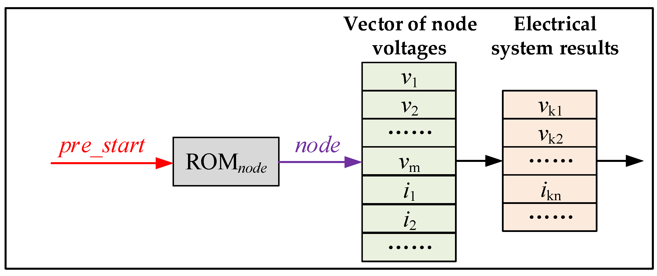
For the electrical system results, in this paper, the modified augmented nodal analysis [39] is applied to solve the electrical system. Both node voltages and branch currents can be obtained by solving the nodal equation. In the FPGA-based real-time simulator, they can be obtained by reading the corresponding node numbers. The number of each node is often different, due to the different structure of ADNs, and therefore the electrical system simulation result output module needs to be universally designed, as shown in Figure 4. In the preload process, the corresponding node numbers are read out from the ROM of the measurement element. Then, the electrical system results corresponding to the node numbers are taken out to form a register set. In this way, the results of the electrical system are obtained, and the universal design of the electrical system result output module can be realized.
For the control system results, the register set of the control system can be obtained by drawing the corresponding registers directly. In the ADNs with the same DGs, the registers don’t need to be modified in different simulation cases.
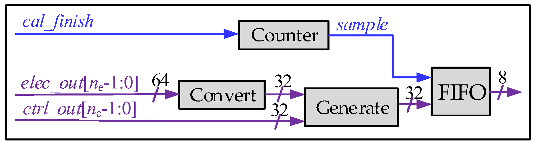
The design of the simulation result output module is shown in Figure 5. The numbers at the port in the figure represent the bit widths of the data signals. The parameters that can be set include the number of the electrical system output results , the number of the control system output results , the maximum number of the output results that can be transmitted to the host PC via Ethernet module , satisfying . denotes the output results sampling interval.
The electrical system output results elec_out and the control system output results ctrl_out are transmitted to the simulation result output module in the form of register sets. The sampling counter counts the completed step number since the last sampling. The sampling signal sample is set to the high level when the counter value is equal to . At this point, the double-precision floating-point electrical system output results are converted to single-precision floating-point by the floating-point conversion module Convert. Then, the output register set can be formed by combining the output results of the electrical system and the control system in the module Generate. The finite state machine is used to store the output results in the FIFO (first in first out) cache in the form of the pipeline. Finally, the output results are sent to the host PC via Ethernet.
4. Case Study
4.1. Simulation Platform
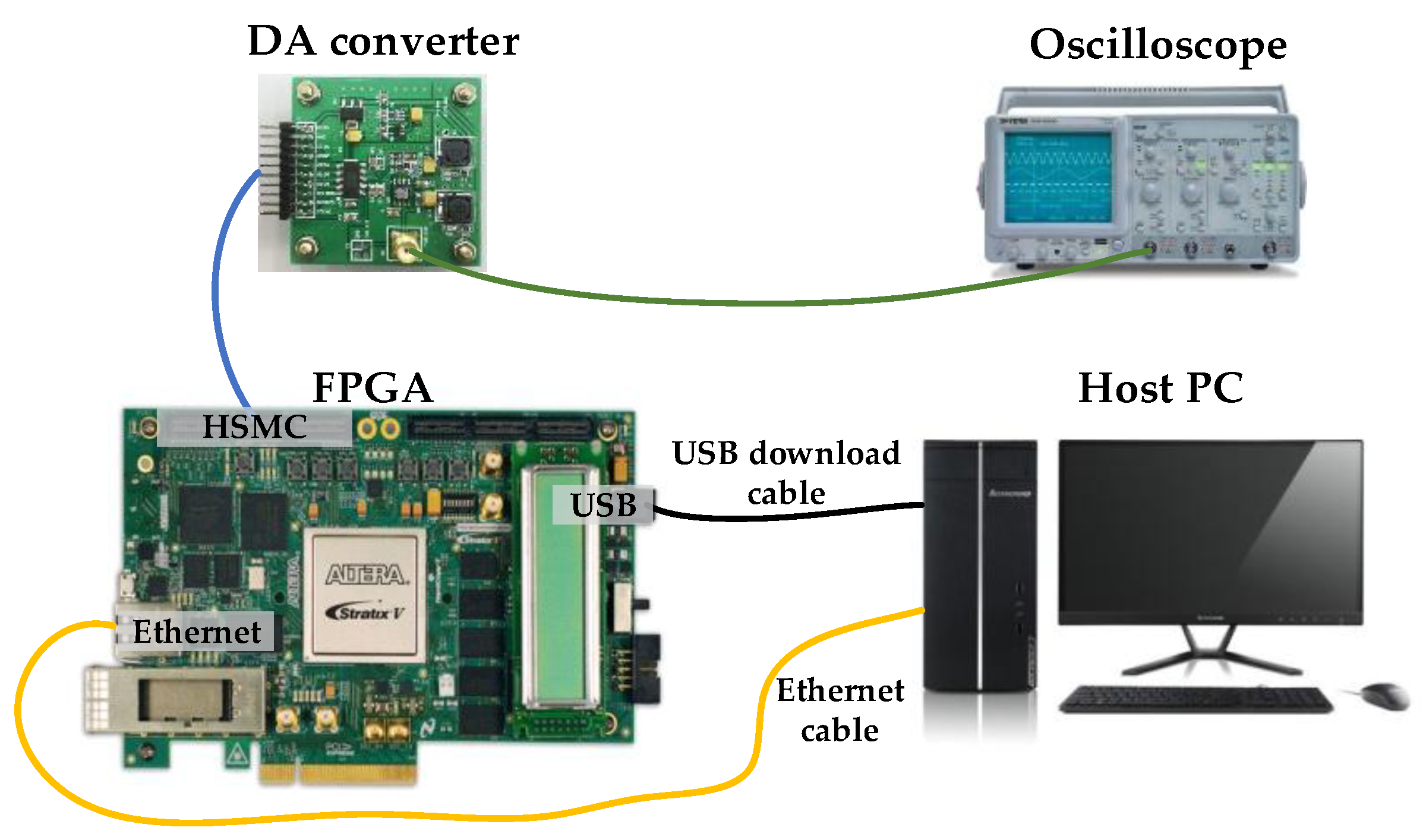
The FPGA-based real-time simulator for ADNs is shown in Figure 6. Stratix® V Edition DSP development kit from Altera® is utilized as the carrier of the real-time simulator, and the manufacturing part number of the FPGA device is 5SGSMD5K2F40C2N. The FPGA-based real-time simulator is driven by a 125 MHz clock. The host PC is a microcomputer with conventional configuration, and the hardware environment is Intel® Xeon® E5-2630 v3 2.40 GHz processor and 24.0 GB memory.
When a case is modified online, the file storing the information of the case is downloaded to the FPGA via the USB interface. The simulation results are uploaded to the host PC via Ethernet interface for real-time storage and display, or displayed on an oscilloscope via an HSMC interface via a digital-to-analog (DA) converter.
4.2. Test Case 1
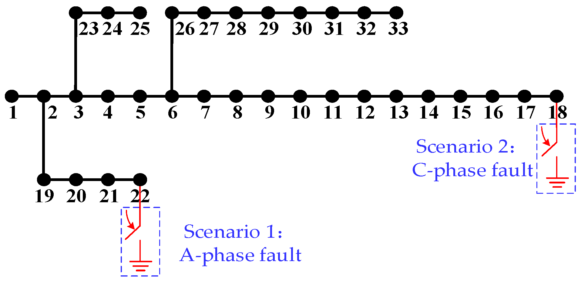
To verify the correctness and effectiveness of the universal design of the FPGA-based real-time simulator for ADNs, the simulator is adapted to conduct the multi-scene transient simulation of the distribution network in this test case. The IEEE 33-node system [40] is shown in Figure 7.
In Scenario 1, it is assumed that an A-phase grounding short circuit fault occurs at 2.0 s on node 22, and the fault is removed at 2.2 s. A simulation time-step of 5 μs is specified. In Scenario 2, it is assumed that a C-phase grounding short circuit fault occurs at 1.6 s on node 18, and the fault is removed at 1.8 s. A simulation time-step of 8 μs is specified. All the faults are simulated by breaker elements. The dimensions of linear equations are both 108 dimensions. With different simulation steps, element parameters and node numbers of the two scenarios, the correctness and effectiveness of the universal design without recompiling proposed in this paper can be verified.
For distribution network without DGs and their control systems, when the dimension of linear equations is 110, it occupies 98% of logic resources, 16% of memory resources and 30% of DSP modules. Therefore, the maximum dimension of the system of linear equations that can be simulated is set to 110 dimensions. It is worth mentioning that, for the simulation of larger systems, the multi-FPGA-based real-time simulator [25] can be used. The proposed universal design is extensible, and it will be applied in the multi-FPGA-based real-time simulator in future work.
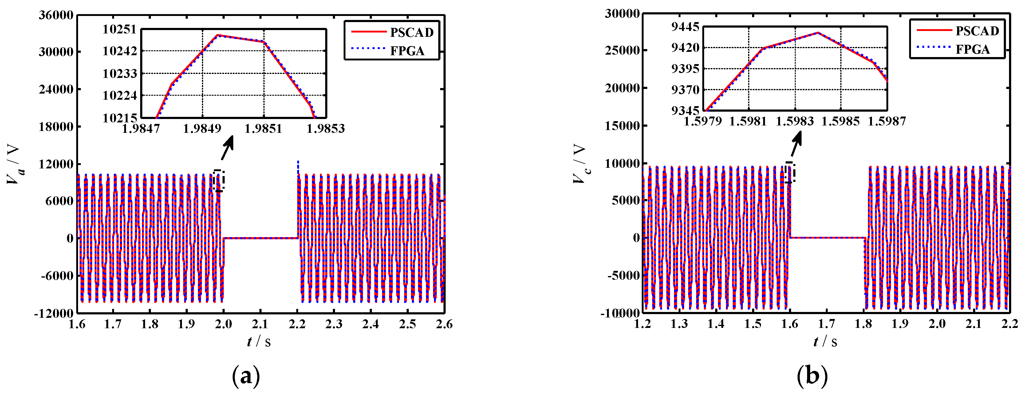
The simulation results of the proposed universal FPGA-based real-time simulator and commercial software PSCAD/EMTDC are compared, as shown in Figure 8. The simulation time-steps of 5 μs and 8 μs are adopted respectively in PSCAD/EMTDC. The simulation calculation time is set to 4 s. Firstly, Scenario 1 is implemented in both real-time simulators. The simulation results are shown in Figure 8a. It can be seen that the results obtained by the two simulators are basically the same, which proves the correctness of the proposed universal design of the FPGA-based simulator. Then, without modifying the design of the simulator and recompiling, the case run in the simulator is updated online as Scenario 2. The simulation results are shown in Figure 8b. It is shown that the simulation results are identical, which verifies the effectiveness of the universal function of the simulator. The results further demonstrate that the FPGA-based real-time simulator has the ability of reconfigurable computing, and users can simulate new cases without recompiling.
The comparison of simulation time between the universal FPGA-based real-time simulator and the conventional FPGA-based real-time simulator is shown in Table 1. The above test is carried out in both simulators. It can be seen that the adoption of the universal FPGA-base real-time simulator can save user’s time and greatly improve the simulation efficiency.
This case test process can be mainly used for fault scanning and other cases where multiple scenarios need to be simulated. When more scenes need to be simulated, the universal simulator can save more time. In contrast, for the conventional simulator, it takes several hours to compile every time the simulation scenario is changed. Therefore, the simulation efficiency can be better improved by the proposed universal real-time simulator.
4.3. Test Case 2
In this test case, the transient process of the distributed generator and the active distribution network is analyzed based on the simulator. For active distribution networks with a PV, when the dimension of the linear equations is 88, 99% of logic resources, 14% of memory resources and 26% of DSP modules are occupied. Thus, the maximum dimension of the linear equations that can be simulated is 88.
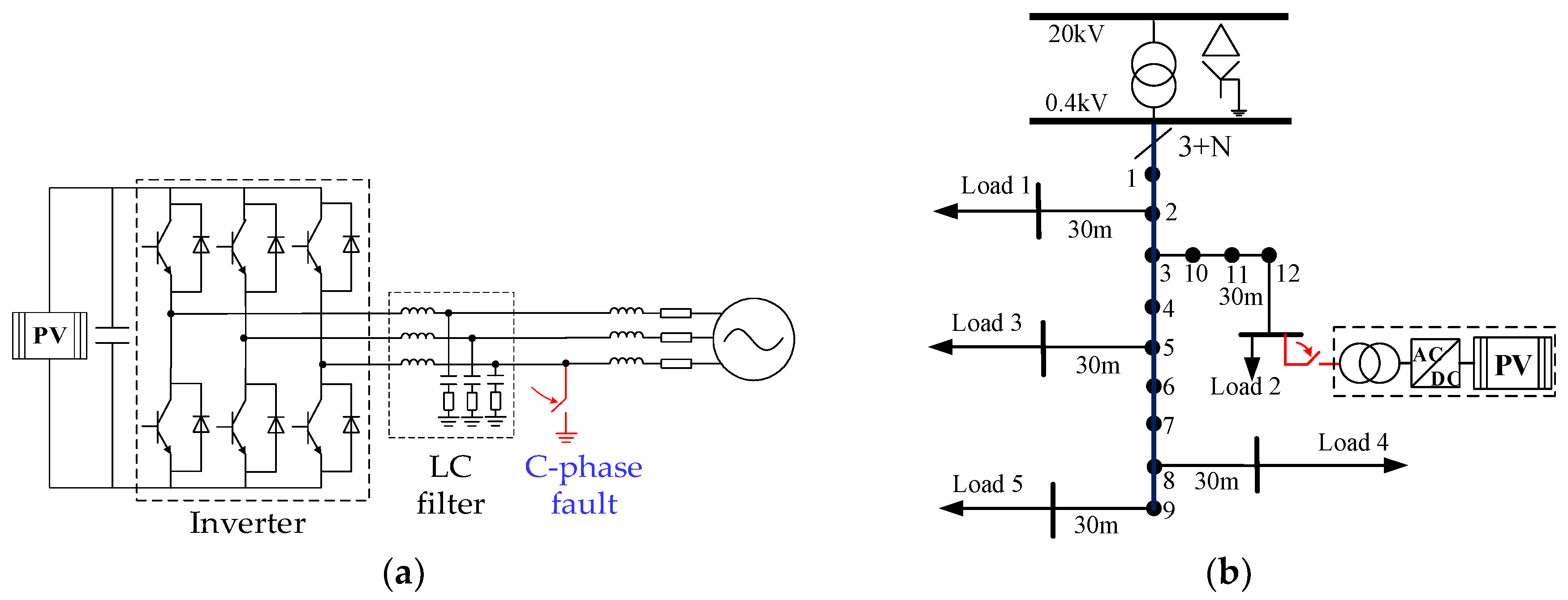
Figure 9 shows the structure of the ADNs. The same simulation time-steps as the FPGA-based real-time simulator is adopted by PSCAD/EMTDC, respectively.
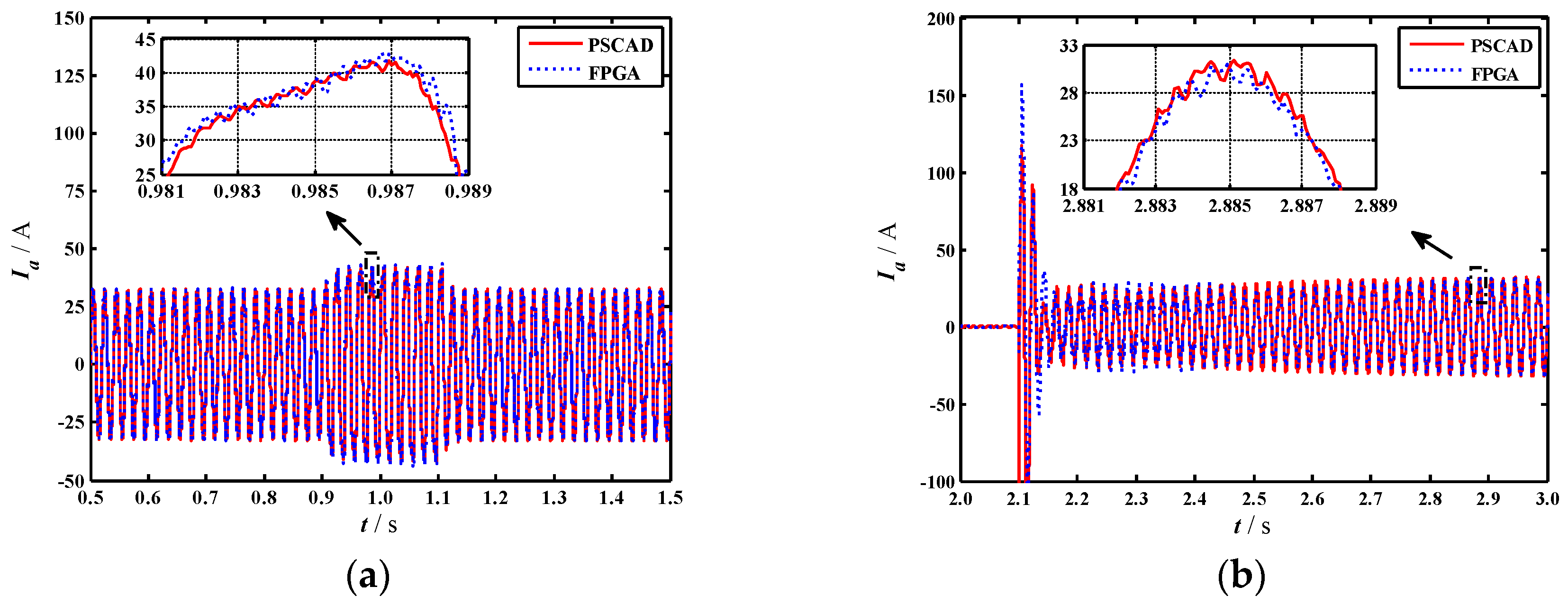
The transient process of the PV in scenario 1 is simulated firstly. As shown in Figure 9a, a unipolar photovoltaic unit is connected to an infinite bus in scenario 1. In the photovoltaic unit, the inverter is controlled by the - control strategy. The reference value of the photovoltaic voltage is 350 V, the temperature is 298 K, and the is 0var, which ensures the operation of unit power factor. The simulation time-step is 2 μs, and the dimension of linear equations is 21 dimension. It is assumed that C-phase grounding fault occurs at the grid-connected point of the photovoltaic cell at 0.9 s and the fault is removed at 1.1 s. The simulation results are shown in Figure 10a.
Then, the transient grid connecting process in Scenario 2 is simulated. As shown in Figure 9b, the test system is an active distribution network with a PV. The transformer and source are represented by a constant impedance in series with a voltage source. The detailed parameters of the distribution network can refer to Reference [41]. The simulation time-step is 3 μs, and the dimension of linear equations is 85 dimension. In the beginning, the circuit breaker between the PV and the distribution network is disconnected, and the PV is connected to the grid at 2.1 s. The simulation results are shown in Figure 10b.
The comparison of simulation time between the universal FPGA-based real-time simulator and the conventional FPGA-based real-time simulator is shown in Table 2. It can be seen that the proposed universal FPGA-base real-time simulator has high simulation efficiency.
On this basis, the parameters of the test case can be modified and updated online without recompiling to study the dynamic of the whole ADN after the DG is connected to the distribution network. This is beyond the scope of this paper and will not be further presented.
4.4. Test Case 3
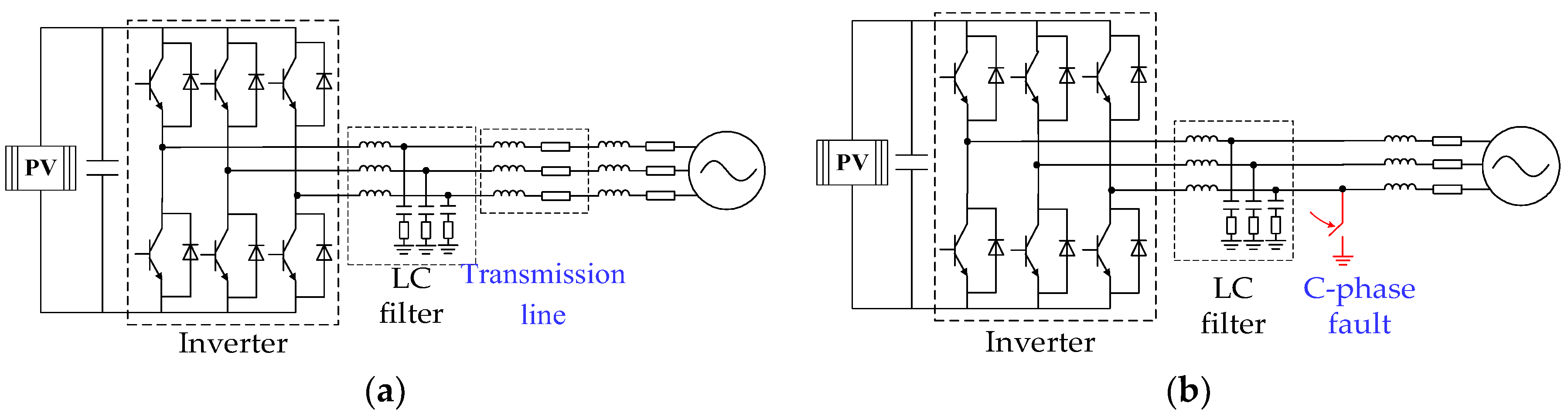
In this test case, another type of application of the universal FPGA-based real-time simulator is presented. As a DG with detailed modeling, there are many parameters that need to be continuously debugged, especially when the hardware-in-the-loop simulation is required. It is necessary to repeatedly modify the parameters for debugging according to the simulation results. To illustrate the application of parameter debugging, test cases of the PV are simulated in the simulator, as is shown in Figure 11.
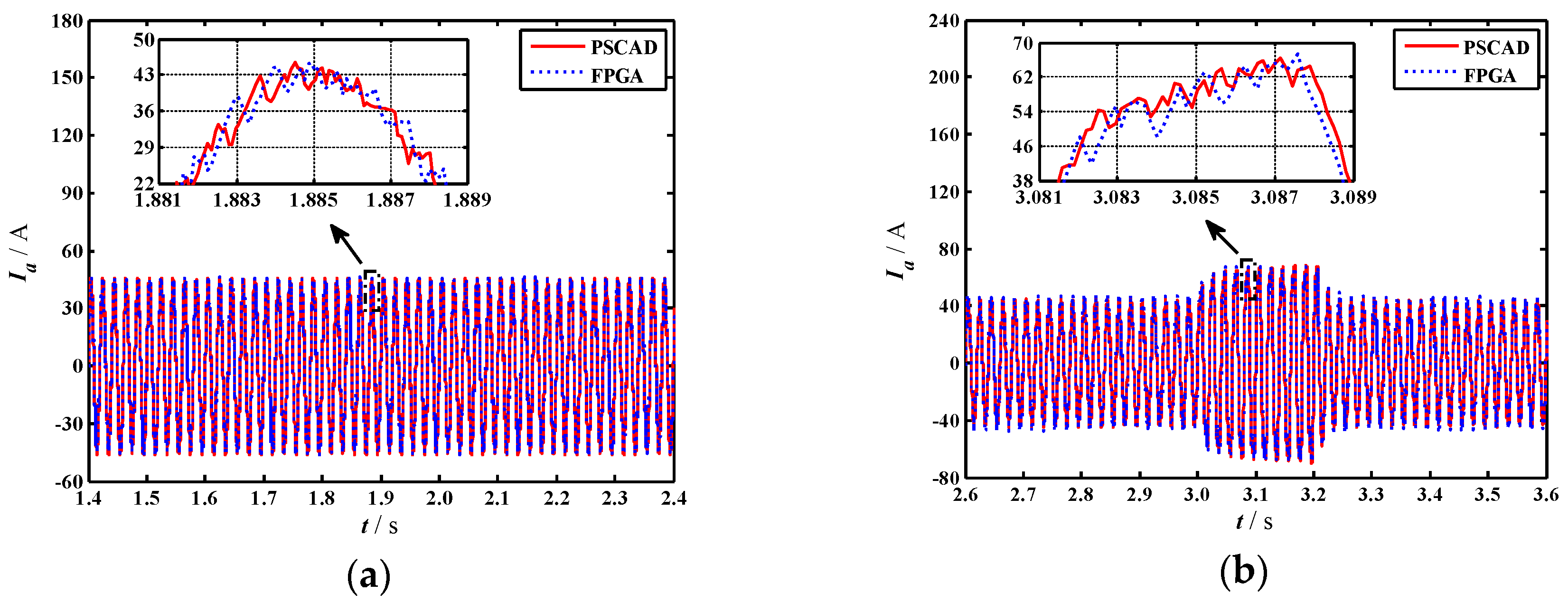
Two scenarios are given in this test case. (1) The simulation time-steps of the two scenarios are different. The simulation time-step of Scenario 1 is 3 μs, and the simulation time-step of Scenario 2 is 5 μs, which means that users can modify the simulation time-step as needed during debugging. (2) The two scenarios have different fault conditions. Scenario 1 has no faults, and Scenario 2 has a fault, which means that users can add faults to the system at any time according to needs, and can modify the fault occurrence time in real time. (3) The topologies of the two scenarios are different. A section of the transmission line is added in Scenario 2, which can help us observe the situation of the DG access to different topologies. Modifying the simulation time-step, modifying the location and occurrence time of the fault, and adjusting the topology are the functions we need to debug parameters of DGs. These functions can be achieved in the real-time simulator using this universal design method. Users can instantly adjust the parameters according to the simulation results and obtain the simulation results immediately.
The comparison of simulation time is the same as that in Test Case 2. The simulation results are shown in Figure 12. It can be seen that the simulation results of the two simulation tools are nearly the same, which verifies the correctness and effectiveness of the proposed universal design.
What needs to be mentioned is that the cost of the simulators is indeed an important factor to consider. We selected the widely-used simulator RTDS as a representative of commercial real-time simulators. The real-time simulator based on single-chip FPGA in this paper can simulate up to three PV units, and the same work needs to consume multiple gigabit processor cards (GPCs) in RTDS. Therefore, the FPGA-based real-time simulator is more cost-effective.
5. Conclusions
The FPGA-based real-time simulator for active distribution networks makes full use of the advantage of parallel computation of FPGA, which can well meet the demand of real-time simulation of ADNs. In this paper, the idea of reconfigurable computing is used to realize the universality of the FPGA-based real-time simulator. This paper aims to optimize the offline preparation process so that the recompiling time is saved, which enhances the flexibility of the usage. The universal design is carried out in detail for the modules that limit the universality. It mainly includes the following aspects.
- The universal design of the parameter configuration and the initial value setting is proposed. In the preload process, the simulation parameters are configured, and the memories are initialized. Therefore, it’s unnecessary to compile the FPGA design when the simulation case is modified or changed.
- The universal design of the linear equations solving module is proposed. A margin for the linear equation solving module is introduced, so that the cases can be modified to some extent and simulated consecutively without recompiling.
- The universal design of the simulation result output module is proposed. The output results can be obtained by reading the corresponding node numbers from the ROM of the measurement element, and the output results can be adaptive to change with the user’s choice.
The proposed universal design enables the simulator to have the ability of reconfigurable computing. The simulation cases can be modified and updated online without changing the FPGA design and recompiling, which improves the simulation efficiency of the FPGA-based real-time simulator. The correctness and effectiveness of the universal design are verified by the simulation cases of the ADNs.
Author Contributions
S.J., H.Y. and X.F. conceived and designed the study. S.J. and H.Y. performed the study. S.J. and Z.W. analyzed the results. S.J. drafted this article. X.F., K.Y. and P.L. made the critical and final reviewing.
Funding
This research was funded by the National Natural Science Foundation of China, grant 51577127 and the Technology Project of State Grid, grant PD71-16-005.
Conflicts of Interest
The authors declare no conflict of interest.
References
- Yan, B.; Wang, B.; Zhu, L.; Liu, H.; Liu, Y.; Ji, X.; Liu, D. A novel, stable, and economic power sharing scheme for an autonomous microgrid in the energy internet. Energies 2015, 8, 12741–12764. [Google Scholar] [CrossRef]
- Li, P.; Ji, H.; Wang, C.; Zhao, J.; Song, G.; Ding, F.; Wu, J. Coordinated control method of voltage and reactive power for active distribution networks based on soft open point. IEEE Trans. Sustain. Energy 2017, 8, 1430–1442. [Google Scholar] [CrossRef]
- Lopes, J.A.P.; Hatziargyriou, N.; Mutale, J.; Djapic, P.; Jenkins, N. Integrating distributed generation into electric power systems: A review of drivers, challenges and opportunities. Electr. Power Syst. Res. 2007, 77, 1189–1203. [Google Scholar] [CrossRef] [Green Version]
- Li, P.; Ji, H.; Wang, C.; Zhao, J.; Song, G.; Ding, F.; Wu, J. Optimal operation of soft open points in active distribution networks under three-phase unbalanced conditions. IEEE Trans. Smart Grid 2019, 10, 380–391. [Google Scholar] [CrossRef]
- Xyngi, I.; Ishchenko, A.; Popov, M.; van der Sluis, L. Transient stability analysis of a distribution network with distributed generators. IEEE Trans. Power Syst. 2009, 24, 1102–1104. [Google Scholar] [CrossRef]
- Wang, C.; Fu, X.; Li, P.; Wu, J.; Wang, L. Multiscale simulation of power system transients based on the matrix exponential function. IEEE Trans. Power Syst. 2017, 32, 1913–1926. [Google Scholar] [CrossRef]
- Hooshyar, H.; Mahmood, F.; Vanfretti, L.; Baudette, M. Specification, implementation, and hardware-in-the-loop real-time simulation of an active distribution grid. Sustain. Energy Grids Netw. 2015, 3, 36–51. [Google Scholar] [CrossRef]
- Mclaren, P.G.; Kuffel, R.; Wierckx, R.; Giesbrecht, J.; Arendt, L. A real time digital simulator for testing relays. IEEE Trans. Power Deliv. 1992, 7, 207–213. [Google Scholar] [CrossRef]
- Bélanger, J.; Lapointe, V.; Dufour, C.; Schoen, L. eMEGAsim: An open high-performance distributed real-time power grid simulator. Architecture and specification. In Proceedings of the International Conference on Power System, Bangalore, India, 12–14 December 2007. [Google Scholar]
- Paré, D.; Turmel, G.; Soumagne, J.C.; Do, V.Q.; Casoria, S.; Bissonnette, M.; Marcoux, B.; McNabb, D. Validation tests of the Hypersim digital real-time simulator with a large AC-DC network. In Proceedings of the International Conference on Power Systems Transients, New Orleans, LA, USA, 28 September–2 October 2003. [Google Scholar]
- Krebs, R.; Ruhle, O. NETOMAC real-time simulator-a new generation of standard test modules for enhanced relay testing. In Proceedings of the Eighth IEE International Conference on Developments in Power System Protection, Amsterdam, The Netherlands, 5–8 April 2004. [Google Scholar]
- Perron, M.; Ghahremani, E.; Heniche, A.; Kamwa, I.; Lafond, C.; Racine, M.; Akremi, H.; Cadieux, P.; Lebeau, S.; Landry, S. Wide-area voltage control system of flexible AC transmission system devices to prevent voltage collapse. IET Gener. Transm. Distrib. 2017, 11, 4556–4564. [Google Scholar] [CrossRef]
- Le-Huy, P.; Sybille, G.; Giroux, P.; Loud, L.; Huang, J.A.; Kamwa, I. Real-time electromagnetic transient and transient stability co-simulation based on hybrid line modelling. IET Gener. Transm. Distrib. 2017, 11, 2983–2990. [Google Scholar] [CrossRef]
- Doorwar, A.; Bhalja, B.; Malik, O.P. A New Internal Fault Detection and Classification Technique for Synchronous Generator. IEEE Trans. Power Deliv. 2019, 34, 739–749. [Google Scholar] [CrossRef]
- Hong, Y.Y.; Wei, Y.H.; Chang, Y.R.; Lee, Y.D.; Liu, P.W. Fault detection and location by static switches in microgrids using wavelet transform and adaptive network-based fuzzy inference system. Energies 2014, 7, 2658–2675. [Google Scholar] [CrossRef]
- Al Jowder, F.A.R.; Ooi, B.T. Series compensation of radial power system by a combination of SSSC and dielectric capacitors. IEEE Trans. Power Deliv. 2005, 20, 458–465. [Google Scholar] [CrossRef]
- Hu, Y.; Wu, W.; Zhang, B.; Guo, Q. Development of an RTDS-TSA hybrid transient simulation platform with frequency dependent network equivalents. In Proceedings of the 2013 4th IEEE/PES Innovative Smart Grid Technologies Europe, Lyngby, Denmark, 6–9 October 2013. [Google Scholar]
- Meka, R.; Sloderbeck, M.; Faruque, M.O.; Langston, J.; Steurer, M.; DeBrunner, L.S. FPGA model of a high-frequency power electronic converter in an RTDS power system co-simulation. In Proceedings of the 2013 IEEE Electric Ship Technologies Symposium, Arlington, VA, USA, 22–24 April 2013. [Google Scholar]
- Dufour, C.; Belanger, J.; Lapointe, V. FPGA-based ultra-low latency HIL fault testing of a permanent magnet motor drive using RT-LAB-XSG. In Proceedings of the Joint International Conference on Power System Technology and IEEE Power India Conference, New Delhi, India, 12–15 October 2008. [Google Scholar]
- Zhang, B.D.; Fu, S.W.; Jin, Z.; Hu, R.Z. A novel FPGA-based real-time simulator for micro-grids. Energies 2017, 10, 1239. [Google Scholar] [CrossRef]
- Zhang, B.D.; Wu, Y.J.; Jin, Z.; Wang, Y. A real-time digital solver for smart substation based on orders. Energies 2017, 10, 1795. [Google Scholar] [CrossRef]
- Chen, Y.; Dinavahi, V. Multi-FPGA digital hardware design for detailed large-scale real-time electromagnetic transient simulation of power systems. IET Gener. Transm. Distrib. 2013, 7, 451–463. [Google Scholar] [CrossRef]
- Matar, M.; Karimi, H.; Etemadi, A.; Iravani, R. A high performance real-time simulator for controllers hardware-in-the-loop testing. Energies 2012, 5, 1713–1733. [Google Scholar] [CrossRef]
- Li, P.; Wang, Z.Y.; Ding, C.D.; Yu, H.; Wang, C.S. A design of grid-connected PV system for real-time transient simulation based on FPGA. In Proceedings of the 2015 IEEE Power and Energy Society General Meeting, Piscataway, NJ, USA, 26–30 July 2015. [Google Scholar]
- Li, P.; Wang, Z.Y.; Wang, C.S.; Fu, X.P.; Yu, H.; Wang, L.W. Synchronisation mechanism and interfaces design of multi-FPGA-based real-time simulator for microgrids. IET Gener. Transm. Distrib. 2017, 11, 3088–3096. [Google Scholar] [CrossRef]
- Gort, M.; Anderson, J. Design re-use for compile time reduction in FPGA high-level synthesis flows. In Proceedings of the 2014 International Conference on Field-Programmable Technology (FPT), Shanghai, China, 10–12 December 2014. [Google Scholar] [CrossRef]
- Sankar, Y.; Rose, J. Trading quality for compile time: Ultra-fast placement for FPGAs. In Proceedings of the ACM/SIGDA Seventh International Symposium on Field Programmable Gate Arrays, Monterey, CA, USA, 21–23 February 1999. [Google Scholar] [CrossRef]
- Chen, Y. Large-Scale Real-Time Electromagnetic Transient Simulation of Power Systems Using Hardware Emulation on FPGAs. Ph.D. Thesis, University of Alberta, Edmonton, AB, Canada, 2012. [Google Scholar]
- Wang, C.S.; Ding, C.D.; Li, P.; Yu, H. Real-time transient simulation for distribution systems based on FPGA, Part II: System architecture and algorithm verification. Proc. CSEE 2014, 34, 628–634. [Google Scholar] [CrossRef]
- Behnke, M.; Ellis, A.; Kazachkov, Y.; McCoy, T.; Muljadi, E.; Price, W.; Sanchez-Gasca, J. Development and validation of WECC variable speed wind turbine dynamic models for grid integration studies. In Proceedings of the AWEA’s 2007 Wind Power Conference, Los Angeles, CA, USA, 4–7 June 2007. [Google Scholar]
- Tsai, H.L.; Tu, C.S.; Su, Y.J. Development of generalized photovoltaic model using Matlab/Simulink. In Proceedings of the World Congress on Engineering and Computer Science 2008, San Francisco, CA, USA, 22–24 October 2008. [Google Scholar]
- Estrin, G.; Bussell, B.; Turn, R.; Bibb, J. Parallel processing in a restructurable computer system. IEEE Trans. Electron. Comput. 1964, EC-12, 747–755. [Google Scholar] [CrossRef]
- Dehon, A.; Wawrzynek, J. Reconfigurable computing: What, why, and implications for design automation. In Proceedings of the 36th ACM/IEEE Conference on Design Automation, New Orleans, LA, USA, 21–25 June 1999. [Google Scholar] [CrossRef]
- Watson, N.; Arrillaga, J. Power Systems Electromagnetic Transients Simulation; The Institution of Electrical Engineers: London, UK, 2003; ISBN 978-08-5296-106-3. [Google Scholar]
- Wei, S.J.; Liu, L.B.; Yin, S.Y. Key techniques of reconfigurable computing processor. Sci. Sin. Inf. 2012, 42, 1559–1576. [Google Scholar] [CrossRef]
- Compton, K.; Hauck, S. Reconfigurable computing: A survey of systems and software. ACM Comput. Surv. 2002, 34, 171–210. [Google Scholar] [CrossRef]
- Wang, C.S.; Ding, C.D.; Li, P.; Yu, H. Real-time transient simulation for distribution systems based on FPGA, Part I: Module realization. Proc. CSEE 2014, 34, 161–167. [Google Scholar] [CrossRef]
- Dommel, H.W. Digital computer solution of electromagnetic transients in single-and multiphase networks. IEEE Trans. Power Appl. Syst. 1969, 4, 388–399. [Google Scholar] [CrossRef]
- Li, P.; Wang, C.S.; Huang, B.B.; Gao, F.; Ding, C.D.; Yu, H. Methodology of transient simulation in time domain for DG and microgrid (1): Basic framework and algorithm. Electr. Power Autom. Equip. 2013, 33, 33–39. [Google Scholar] [CrossRef]
- Baran, M.E.; Wu, F.F. Network reconfiguration in distribution systems for loss reduction and load balancing. IEEE Trans. Power Deliv. 1989, 4, 1401–1407. [Google Scholar] [CrossRef]
- Papathanassiou, S.; Hatziargyriou, N.; Strunz, K. A benchmark low voltage microgrid network. In Proceedings of the GIGRE Symposium, Athens, Greece, 13–16 April 2005. [Google Scholar]
Figure 1.
Structure of the field programmable gate array (FPGA)-based real-time simulator.

Figure 2.
Design of electrical system parameter information configuration.

Figure 3.
Design of the simulation initial value setting.

Figure 4.
Design of the electrical system simulation result output module.

Figure 5.
Design of the simulation result output module.

Figure 6.
The FPGA-based real-time simulator for active distribution networks.

Figure 7.
Test case of the distribution network.

Figure 8.
Comparison of the simulation results between the FPGA-based real-time simulator and PSCAD/EMTDC. (a) A phase voltage of node 22 in Scenario 1. (b) C phase voltage of node 18 in Scenario 2.
Figure 8.
Comparison of the simulation results between the FPGA-based real-time simulator and PSCAD/EMTDC. (a) A phase voltage of node 22 in Scenario 1. (b) C phase voltage of node 18 in Scenario 2.

Figure 9.
Test cases of the active distribution networks. (a) Scenario 1: The PV connected with the infinite bus system. (b). Scenario 2: The active distribution network with a PV.
Figure 9.
Test cases of the active distribution networks. (a) Scenario 1: The PV connected with the infinite bus system. (b). Scenario 2: The active distribution network with a PV.

Figure 10.
Comparison of the simulation results between the FPGA-based real-time simulator and PSCAD/EMTDC. (a) A phase current of the grid-connected point of the PV in Scenario 1. (b) A phase current of the grid-connected point of the PV in Scenario 2.
Figure 10.
Comparison of the simulation results between the FPGA-based real-time simulator and PSCAD/EMTDC. (a) A phase current of the grid-connected point of the PV in Scenario 1. (b) A phase current of the grid-connected point of the PV in Scenario 2.

Figure 11.
Test cases of the PV. (a) Scenario 1: The PV connected with the infinite bus system. (b) Scenario 2: The PV connected with the infinite bus system via a section of the transmission line.
Figure 11.
Test cases of the PV. (a) Scenario 1: The PV connected with the infinite bus system. (b) Scenario 2: The PV connected with the infinite bus system via a section of the transmission line.

Figure 12.
Comparison of the simulation results between the FPGA-based real-time simulator and PSCAD/EMTDC. (a) A phase current of the grid-connected point of the PV in Scenario 1. (b) A phase current of the grid-connected point of the PV in Scenario 2.
Figure 12.
Comparison of the simulation results between the FPGA-based real-time simulator and PSCAD/EMTDC. (a) A phase current of the grid-connected point of the PV in Scenario 1. (b) A phase current of the grid-connected point of the PV in Scenario 2.


Table 1.
Comparison of simulation time between the universal FPGA-based real-time simulator and the conventional FPGA-based real-time simulator.
Table 1.
Comparison of simulation time between the universal FPGA-based real-time simulator and the conventional FPGA-based real-time simulator.
| Type of Simulator | Compile Time | Calculation Time |
|---|---|---|
| Universal simulator | 0 | 4 s |
| Conventional simulator | 3 h 44 min 18 s | 4 s |
Table 2.
Comparison of simulation time between the universal FPGA-based real-time simulator and the conventional FPGA-based real-time simulator.
Table 2.
Comparison of simulation time between the universal FPGA-based real-time simulator and the conventional FPGA-based real-time simulator.
| Type of Simulator | Compile Time | Calculation Time |
|---|---|---|
| Universal simulator | 0 | 4 s |
| Conventional simulator | 4 h 21 min 21 s | 4 s |
© 2019 by the authors. Licensee MDPI, Basel, Switzerland. This article is an open access article distributed under the terms and conditions of the Creative Commons Attribution (CC BY) license (http://creativecommons.org/licenses/by/4.0/).
Share and Cite
MDPI and ACS Style
Jin, S.; Yu, H.; Fu, X.; Wang, Z.; Yuan, K.; Li, P. A Universal Design of FPGA-Based Real-Time Simulator for Active Distribution Networks Based on Reconfigurable Computing. Energies 2019, 12, 2086. https://doi.org/10.3390/en12112086
AMA Style
Jin S, Yu H, Fu X, Wang Z, Yuan K, Li P. A Universal Design of FPGA-Based Real-Time Simulator for Active Distribution Networks Based on Reconfigurable Computing. Energies. 2019; 12(11):2086. https://doi.org/10.3390/en12112086
Chicago/Turabian StyleJin, Shuo, Hao Yu, Xiaopeng Fu, Zhiying Wang, Kai Yuan, and Peng Li. 2019. "A Universal Design of FPGA-Based Real-Time Simulator for Active Distribution Networks Based on Reconfigurable Computing" Energies 12, no. 11: 2086. https://doi.org/10.3390/en12112086
Note that from the first issue of 2016, this journal uses article numbers instead of page numbers. See further details here.