Influence of AlN and GaN Pulse Ratios in Thermal Atomic Layer Deposited AlGaN on the Electrical Properties of AlGaN/GaN Schottky Diodes


1
Department of Visual Optics, Seoul National University of Science and Technology (Seoultech), Seoul 01811, Korea
2
Department of Materials Science and Engineering, Seoul National University of Science and Technology (Seoultech), Seoul 01811, Korea
*
Authors to whom correspondence should be addressed.
Coatings 2020, 10(5), 489; https://doi.org/10.3390/coatings10050489
Submission received: 25 April 2020
/
Revised: 13 May 2020
/
Accepted: 18 May 2020
/
Published: 19 May 2020
(This article belongs to the Special Issue Atomic Layer Deposition of Thin-Films)
Abstract
:Atomic layer deposited AlGaN with different AlN and GaN pulse ratios (2:1, 1:1, and 1:2) was used to prepare AlGaN/GaN Schottky diodes, and their current transport mechanisms were investigated using current–voltage (I–V) and capacitance–voltage (C–V) measurements. Under low reverse bias condition, the sample with the pulse ratio of 2:1 was explained by Poole–Frenkel emission and the negative temperature dependence for the sample with the pulse ratio of 1:2 was associated with the acceptor levels in the AlGaN layer. Fast interface traps at 0.24–0.29 eV were observed for the samples with the pulse ratios of 1:1 and 1:2, whereas bulk traps at ~0.34 eV were observed for the sample with the pulse ratio of 2:1. Higher trap densities were obtained from the C–V hysteresis measurements when the pulse ratios were 1:1 and 1:2, indicating the presence of a charge trapping interfacial layer. According to the X-ray photoelectron spectroscopy spectra, the pulse ratio of 2:1 was found to have less oxygen-related defects in the AlGaN layer.
1. Introduction
Owing to the two-dimensional electron gas (2DEG) formation, AlGaN/GaN structures have been employed to obtain high electron mobility transistors (HEMTs) [1,2,3,4]. For an AlGaN/GaN HEMT, a gate contact with a high Schottky barrier is desirable to reduce gate leakage current and increase breakdown voltages. In scaled down AlGaN/GaN-based devices, the AlGaN barrier should have high Al composition in order to attain high power levels during the high-speed operation [5]. However, strong polarization field as well as high surface state density cause high gate leakage current in these devices [6]. Hence, minimizing the gate leakage current is highly required to enhance the AlGaN/GaN HEMT device performance. In this respect, much research has been carried out to explain the current transport mechanisms governing the leakage current.
Gate leakage current in Al0.28Ga0.72N/GaN HEMTs has been found to increase with the increase of barrier thickness [7]. According to an analytical model for forward bias gate leakage current in an AlGaN/GaN metal–oxide–semiconductor HEMT (MOSHEMT), it was observed that Poole–Frenkel (PF) and trap assisted tunneling (TAT) emission are responsible at a high temperature (T > 388 K), whereas TAT emission becomes dominant at a low temperature (T < 388 K) [8]. PF mechanism was found to rule the conduction through the NiO dielectric layer with an emission barrier of 0.2 eV in AlGaN/GaN diodes [9]. The temperature-dependent reverse leakage currents in Al2O3/Al0.55Ga0.45/GaN structures were associated with the PF emission, related to trap states with activation energies of 0.71, 0.49, and 0.41 eV for high, mid, and low bias regions, respectively [10]. The reverse leakage current for AlGaN/GaN HEMTs with N2 plasma was found to be lower than HCl/H2O solution, which was associated with the shallow traps and the recovery of the Ga–N bond [11].
The most widely used growth technique for obtaining high-quality III-nitride layers is metalorganic chemical vapor deposition (MOCVD) [12]. However, this method employs high growth temperatures (~1000 °C), and thus is incompatible with the complementary metal–oxide–semiconductor (CMOS) technology, temperature-sensitive devices, and flexible substrates. Accordingly, the atomic layer deposition (ALD) growth of III-nitride layers and optimization of the growth process have been researched. Ozgit-Akgun et al. reported on plasma-enhanced ALD-GaN grown at 100–500 °C [13]. Shih et al. reported GaN growth on a Si substrate by remote plasma ALD [14]. Still now, most works have been carried out to investigate ALD grown AlN [15,16,17]. However, ALD growth of AlGaN without the aid of plasma has rarely been investigated [18]. In our previous work, we grew 5 nm thick AlGaN on GaN and investigated the electrical properties of AlGaN/GaN structures [19]. However, the AlN and GaN pulse ratio was fixed as 1:1, thus the effect of AlN and GaN pulse ratio on the AlGaN/GaN structure has not been studied systematically. Therefore, we prepared ALD-AlGaN on GaN substrate with different AlN and GaN pulse ratios and investigated the current transport and charge trapping mechanisms in AlGaN/GaN Schottky diodes.
2. Materials and Methods
As a starting material, we used an n-type, c-plane (0001) GaN substrate (thickness: 325 μm, carrier concentration: 1 × 1017 cm−3). After removing the native oxide layer in an HCl/H2O (1:1) solution, GaN samples were loaded into a thermal ALD chamber (Atomic classic, CN-1, Gyenggi-do, Korea) to grow about 10 nm thick AlGaN thin films at 335 °C. The ALD reaction for AlN subcycle was composed of TMA feeding (0.5 s), N2 purge (5 s), NH3 feeding (5 s), and N2 purge (60 s). Similarly, GaN subcycle was composed of triethylgallium (TEG) feeding (0.3 s), N2 purge (5 s), NH3 feeding (5 s), and N2 purge (60 s). Here, incorporation of GaN for AlGaN films was enabled by combining ALD reactions of AlN and GaN films at different pulse ratios such as 2:1, 1:1, and 1:2 (denoted as samples A, B, and C, respectively). According to Auger electron spectroscopy (AES, ULVAC-PHI, Kanagawa, Japan) analysis, the composition ratios between Al and Ga for all the samples were found to be about 34:6, which corresponds to Al0.85Ga0.15N. Detailed experimental results and its growth mechanism, together with the explanation for the similar composition ratios regardless of the pulse ratios, will be published elsewhere.
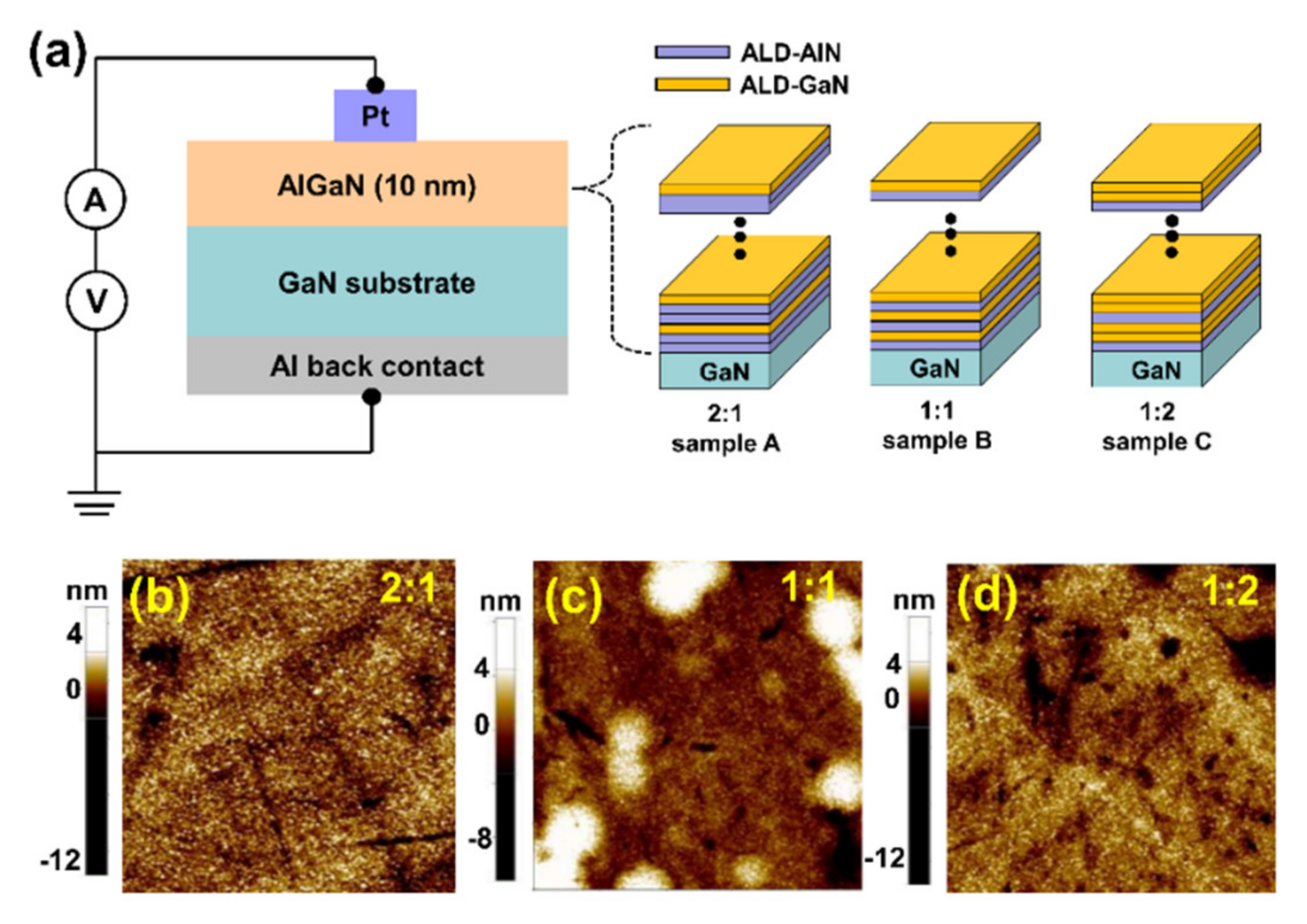
In order to characterize the electrical properties, AlGaN/GaN diodes were fabricated with 50 nm thick Pt Schottky contacts (diameter: 500 μm) and a 100 nm thick Al back contact. Figure 1a shows the schematic layer structure of AlGaN/GaN Schottky devices and the prepared AlGaN layers with different pulse ratios of AlN and GaN. Current–voltage (I–V) characteristics were measured at different temperatures with a Keithley 238 current source (Aldermaston, UK) and capacitance–voltage (C–V) characteristics were measured using an HP 4284A LCR meter (Hewlett Packard, Palo Alto, CA, USA). Figure 1b–d show the atomic force microscopy (AFM, Park Systems, Suwon, Korea) images for the AlGaN layer measured over 2 μm × 2 μm scan areas. The root-mean-square roughness (rms) values for samples A, B, and C were found to be 0.96, 1.98, and 1.19 nm, respectively. The surface became rougher for sample B, as compared with samples A and C. Depth resolved X-ray photoelectron spectroscopy (XPS, ULVAC-PHI, Kanagawa, Japan) measurements with sputter etch treatment were carried out using a monochromatic Al Κα X-ray source to observe the chemical reaction near the AlGaN/GaN interface.
3. Results
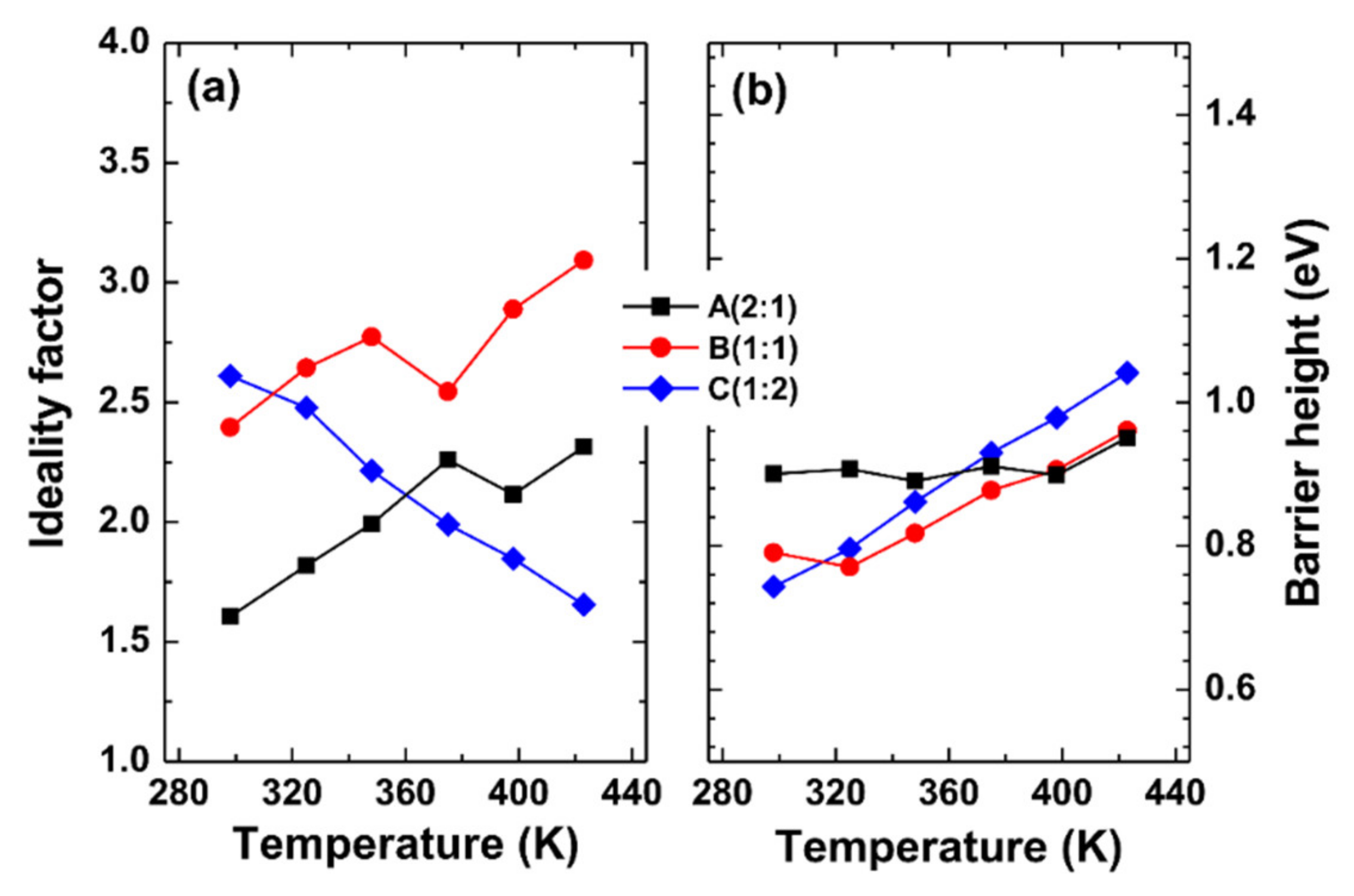
Figure 2 shows the I–V data measured at different temperatures. The increase of reverse current values with increasing the temperature was observed for sample A. This was not observed for samples B and C. In addition, the forward I–V curves for narrow voltage range in the inset in Figure 2c showed the occurrence of crossover at ~0.5 V. Using the thermionic emission (TE) model [20], both the Schottky barrier heights (SBHs) and ideality factors at each temperature were calculated, which are shown in Figure 3. For samples A and B, the ideality factor increased with the temperature. This indicates that the diode quality degraded and other transport mechanisms such as tunneling currents contributed to the current flow. For sample C, the ideality factor decreased and the barrier height increased over the whole temperature range, which can be associated with the lateral barrier inhomogeneity [20].
To clarify the dominant transport mechanism under reverse bias condition, the Poole–Frenkel (PF) emission model was considered first, given by [9,21]
with
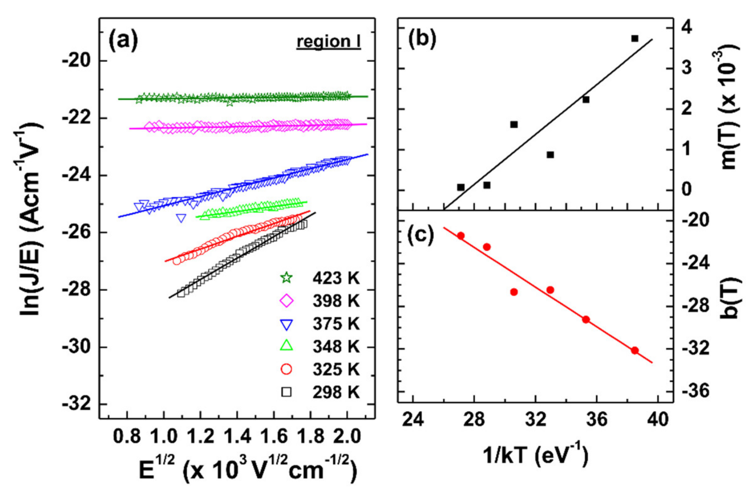
where ε is the relative dielectric permittivity of the gate material at high frequency, ε0 is the permittivity of free space, qϕt is the electron emission barrier height, and C is a constant. For sample A, PF emission was applied to low, mid, and high bias regions (denoted as regions I, II, and III, respectively, in Figure 2a). As an example shown in Figure 4a, the linear fits to the ln(J/E) versus E1/2 plots for region I (−1–−3.5 V) produced both m(T) and b(T) values at each temperature. The dielectric constants for AlN and GaN at high frequency are known to be 4.77 and 5.35, respectively [21], implying that the dielectric constant of AlGaN would be an intermediate value between them. According to the m(T) values shown in Figure 4b, ε was found to be 6.05, which is comparable to the theoretical value. This means that the PF emission is an appropriate current transport mechanism at the low bias region. Using the values of b(T) shown in Figure 4c, qϕt was obtained as 0.93 eV, implying that the defect states localized at 0.93 eV below the AlGaN conduction band are related with the PF emission. This value is similar to the value of 0.9 eV in the previous work on AlGaN/GaN Schottky diodes [22]. It was shown that threading screw dislocations forming trap states with an activation energy of 0.9 eV is the dominant leakage current source in GaN-based devices [23]. Deep level transient spectroscopy studies showed that the electron traps with activation energy of 0.9 eV are associated with extended defects, such as threading dislocations [24]. It is probable that a continuum of electronic states owing to threading dislocations might contribute to the PF emission at the low bias region.
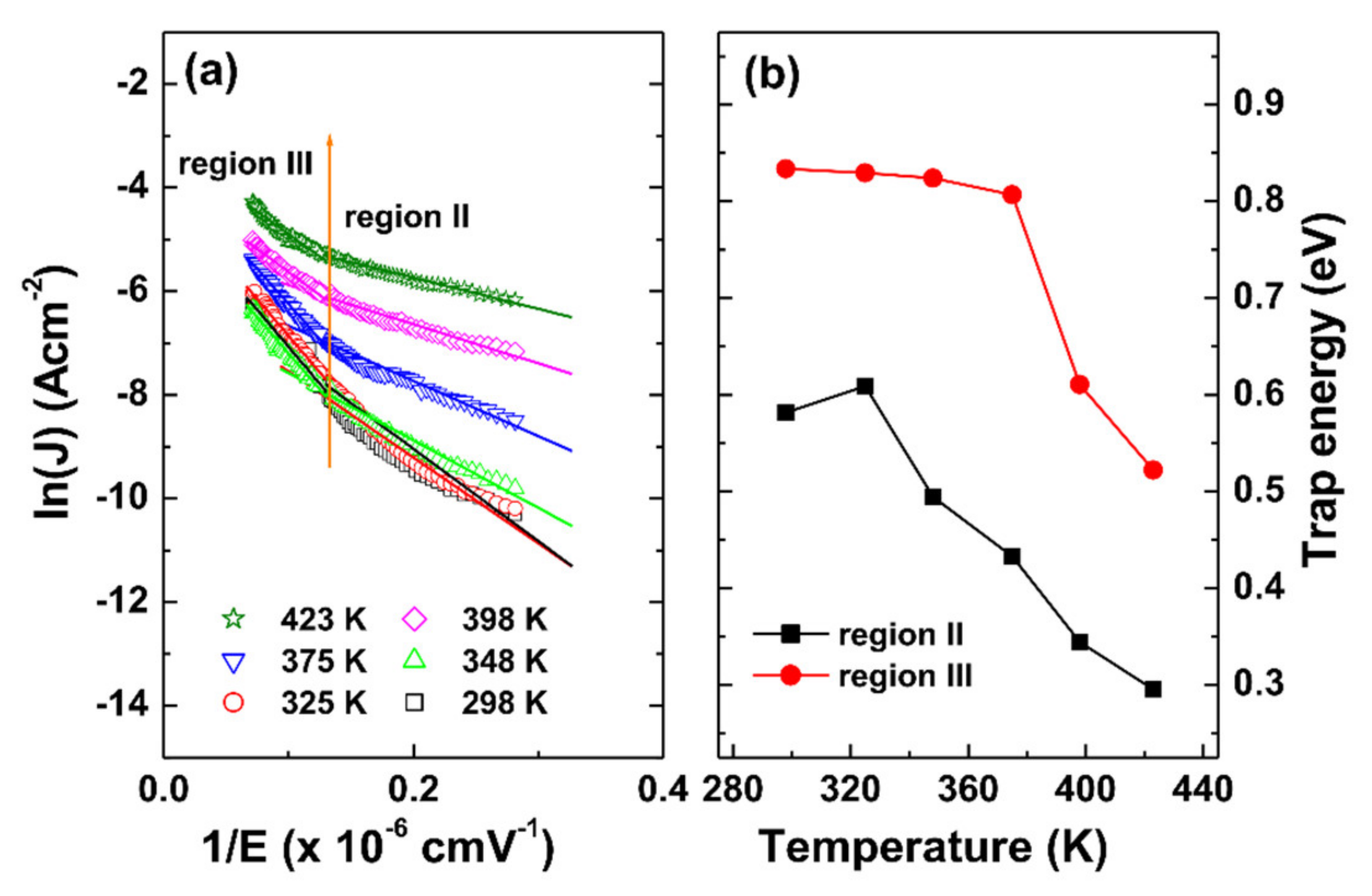
Similarly, PF emission was applied to regions II and III for sample A, and the dielectric constants were found to be 10.02 and 208.38, respectively. These are higher than the theoretical value of the AlGaN layer, indicating that PF emission is inappropriate to explain the current transport. Hence, trap assisted tunneling (TAT) was considered instead. In this model, the current conduction at reverse bias voltage occurs by electron tunneling through the traps existing in the AlGaN barrier layer and the current density for TAT is expressed as [25].
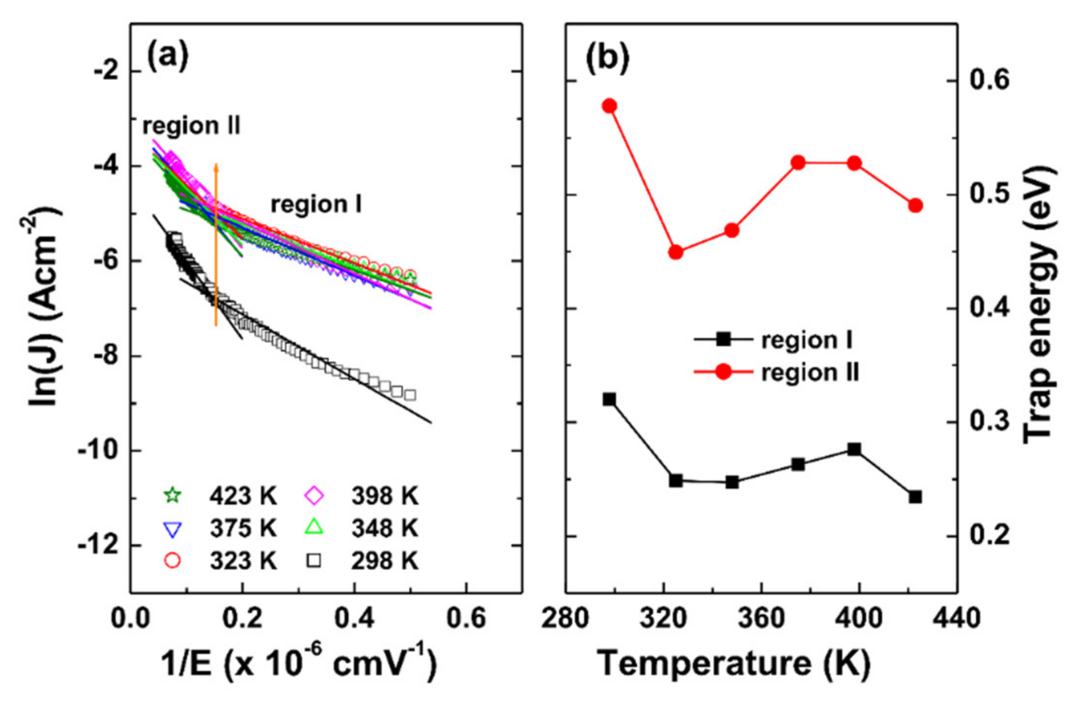
where qϕt is the trap energy level. As shown in Figure 5a, the plots for sample A are composed of two linear regions (denoted as regions II and III in Figure 2a). From the linear fitting to the data, the trap energies at each temperature were obtained, which are shown in Figure 5b. At room temperature, the trap energies were 0.58 and 0.83 eV for regions II and III, respectively. Two trap energies for AlGaN/GaN HEMT were found to be 0.35 and 0.58 eV [26]. The trap energy level in AlGaN/GaN on GaN substrate was deduced to be 0.6–0.7 eV [27], considered to result from the dislocations and nitrogen vacancy (VN) [28]. The energy levels of oxygen substituting for nitrogen (ON) were found to be 0.61 [29] and 0.8 eV [30]. These energy levels are similar to the values of 0.58 and 0.83 eV. Meanwhile, the donor levels at 0.2, 0.5, and 0.9 eV observed in AlN were related to nitrogen vacancies [31]. Although the exact origin is unclear at the present moment, we speculate that ON- and VN-related defects might be responsible for TAT. These trap energies were also found to decrease with the temperature, indicating the temperature enhanced TAT. With the increasing temperature, the electrons have a higher thermal energy, and thus the effective trap energy decreased [32].
As shown in Figure 2b, the reverse current density for sample B is almost constant regardless of the temperature. In this case, PE emission was not appropriate, thus we applied TAT emission to sample B. As shown in Figure 6a, the plots are composed of two linear regions (regions I and II are also indicated in Figure 2b). The obtained trap energies at each temperature are shown in Figure 6b. At room temperature, the trap energies were 0.32 and 0.58 eV for regions I and II, respectively. The variance of the trap energies was not significant compared with sample A. In addition, both samples A and B showed that the extracted trap energies are higher at the high bias region than those at the low bias region. This is because, when the electric field is low, the electrons may tunnel through the trapezoidal barrier. As the reverse bias increases, the electrons may tunnel through the triangular barrier [33].
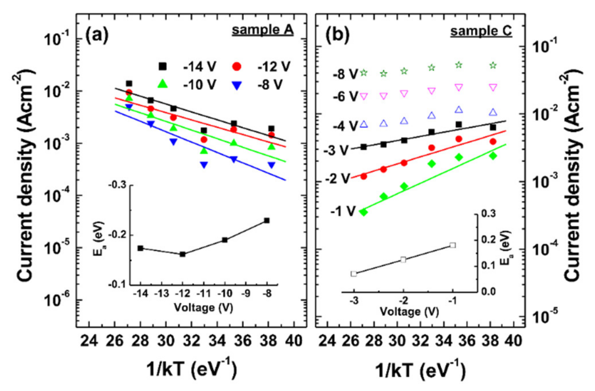
In the TAT mechanism under the high bias region, electrons with an activation energy Ea are thermally activated to the trap states in the barrier layer and tunnel through the barrier. Ea is the activation energy from the Fermi level to trap states. As shown in Figure 2a, the reverse leakage current densities for sample A increase with the temperature, indicating that a thermally activated process is associated. Figure 7a shows the plots of current density versus 1/kT at each bias voltage for sample A. The inset in Figure 7a shows that the extracted activation energies are negative (i.e., positive temperature dependence).
Figure 7b shows the current density at each reverse bias for sample C. At the mid and high bias regions, the current values are almost the same regardless of the temperature, implying that tunneling is the dominant transport mechanism. However, the decrease of reverse leakage current with the increase temperature was observed at the low bias region (−1–−3 V). The positive activation energies at each bias (i.e., negative temperature dependence) were obtained, which are shown in Figure 7b. Arulkumaran et al. found that, in AlGaN/GaN HEMTs, the leakage current decreased with an activation energy of +0.61 eV up to the temperature of 80 °C, and they attributed this to the occurrence of deep acceptor initiated impact ionization [34]. The two-dimensional device simulation in InAlAs/InGaAs HEMTs revealed that the increase of surface trap density at the recess region between gate and drain enhanced the weak impact ionization at low bias voltages [35]. Studies on the influence of various cap layers in AlGaN/GaN HEMTs have shown the following positive activation energies (i.e., negative temperature dependence of drain leakage current). One is deep acceptor-related trap level at +0.395 eV in the HEMTs without cap layers, and the other is two activation energy levels at +0.143 and +0.064 eV in the HEMTs with p-GaN cap layers owing to the effect of Mg atoms (acceptors) [36]. As a result, the decrease of leakage current with increasing the temperature was associated with the deep acceptor initiated impact ionization. In other words, the acceptor levels in the AlGaN layer for sample C might cause the negative temperature dependence in the gate leakage current at low bias. One of the favorable point defects in AlN are Al vacancies (VAl) [30]. These Al vacancies are known to act as acceptors in high Al-content AlGaN [37]. This probably indicates that the formation of Al vacancies occurred more easily for sample C. Resultantly, the favorable defects and their distributions in the AlGaN layer would be different according to the pulse ratios.
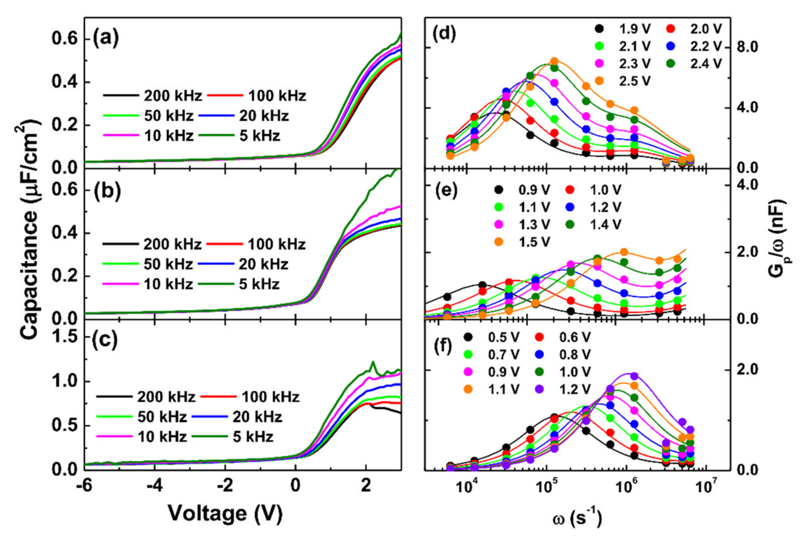
Figure 8a–c show the C–V data obtained at different frequencies. For all three samples, the frequency dispersion was observed in both the depletion and accumulation regions. For x = 0.85, the theoretical dielectric constant of AlGaN layer was found to be ε = 9.5 − 0.5x ≈ 9.08 [38]. Using the equation ε = CAlGaNd/ε0A, the effective dielectric constant of AlGaN layer was calculated. Here, CAlGaN is the measured accumulation capacitance at 100 kHz, d is the thickness of AlGaN, and A is the effective contact area. The obtained values are 5.8, 5.0, and 8.4, for samples A, B, and C, respectively. The lower dielectric constant than the theoretical value might be caused by lower film density of AlGaN layer.
The conductance method was used to determine the trap density. The parallel conductance (Gp/ω) versus radial frequency (ω = 2πf) plots are described through the following equation [39]
where DT and τT are trap density and trap response time, respectively. Figure 8d–f show the fitting and experimental data. On the basis of the Shockley–Read–Hall statistics [38], the trap energy level below the GaN conduction band (i.e., denoted as EC − Et) was calculated from τT [39]
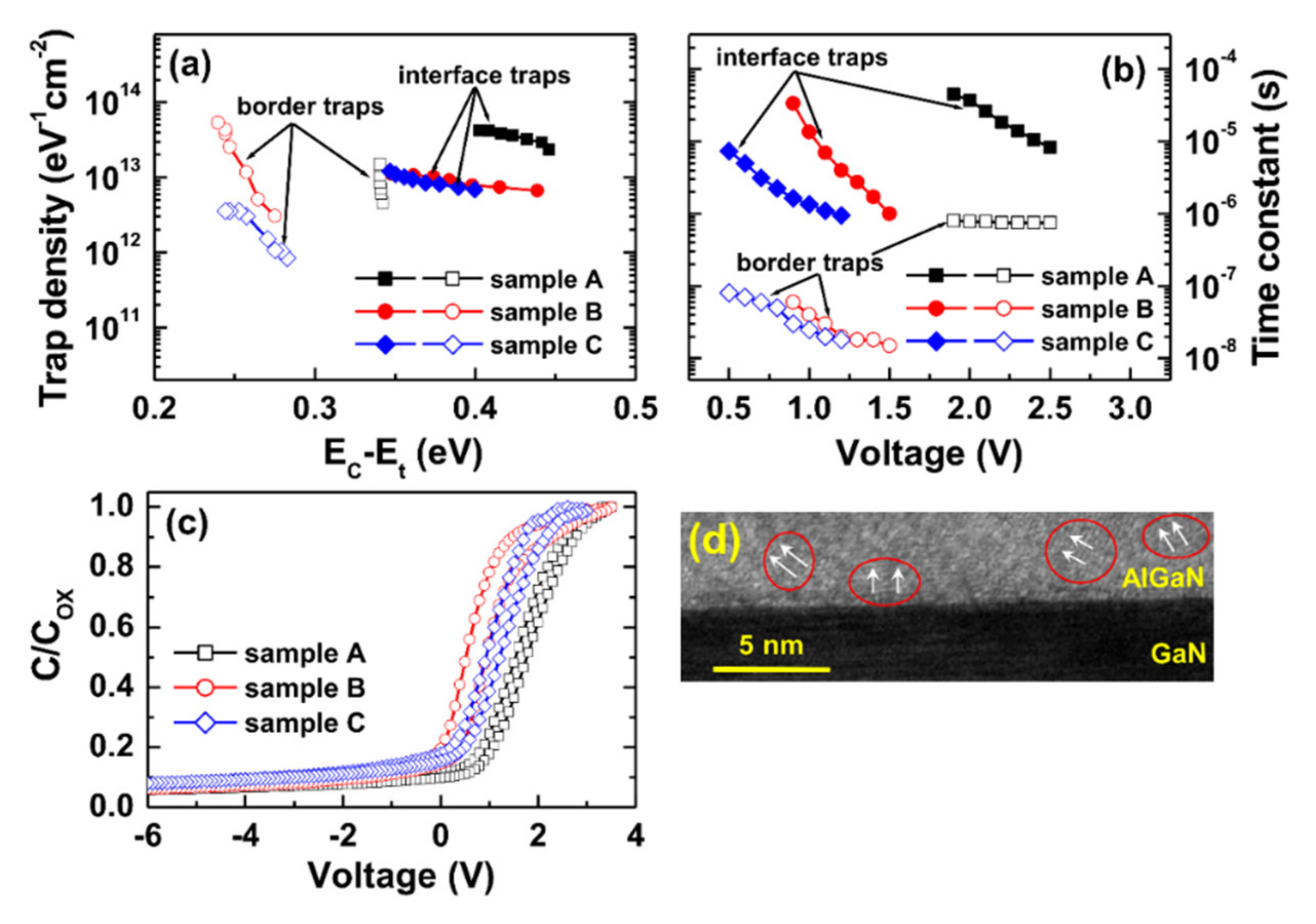
where vth, σn, and NC are the thermal velocity, the electron capture cross section, and the effective density of states in the conduction band of GaN, respectively. Using the values of vth = 2.6 × 107 cm·s−1, σn = 4 × 10⁻¹³ cm2, and NC = 2.2 × 1018 cm−3 [40], the trap densities and the time constants were calculated, which are shown in Figure 9a,b, respectively. The interface and bulk traps have different features in time constant. For the interface traps, the time constant reveals an exponential dependence on the applied voltage. On the contrary, the time constant for the bulk traps is insensitive to the bias voltage [41,42]. The interface traps distributed at 0.35–0.45 eV with the slow time constants between 1 and 50 μs were observed. For these traps, sample A showed the highest values. Relatively narrow energy distribution at 0.24–0.29 eV with the low time constants between 0.02 and 0.08 μs were observed for samples B and C, implying the fast interface traps. Whereas the border traps at ~0.34 eV were observed for sample A with the maintained time constant of 0.8 μs.
Figure 9c shows the C–V hysteresis curves obtained at 100 kHz. All the samples showed the positive shift in the flatband voltage (). Using ΔVFB values, the trapping electron state density (QT) was calculated through the equation as follows [43,44]
where COX is the measured accumulation capacitance. The trap densities were estimated to be about 7.89 × 10¹¹, 1.33 × 10¹², and 1.43 × 1012 cm−2 for samples A, B, and C, respectively. The hysteresis in the C–V measurement may be attributable to the interface states of AlGaN/GaN and oxide traps in the AlGaN layer. In the metal–insulator–semiconductor structure, the associated traps arise from the oxidized transition layer with poor crystalline quality and a disordered structure, which induces the C–V hysteresis owing to their different electron capture and emission time during the measurement [42]. Figure 9d shows the cross-sectional scanning transmission electron microscope (STEM, JEOL/CEOS, Tokyo, Japan) image near the AlGaN/GaN interface for sample B, revealing the polycrystalline structure for AlGaN layer. The TEM image also indicates that the remained native oxide layer is hardly observed. Hence, the interfacial oxide layer causing charge trapping might be formed during the ALD process. Furthermore, our recent work has shown the effective passivation effect on GaN Schottky contacts using 2 nm thick AlN, which was associated with the generation of many Al–O–N bonds near the AlN/GaN interface [45]. As a result, it can be speculated that the formation of the oxidized transition layer near the AlGaN/GaN interface was suppressed for sample A compared with other samples.
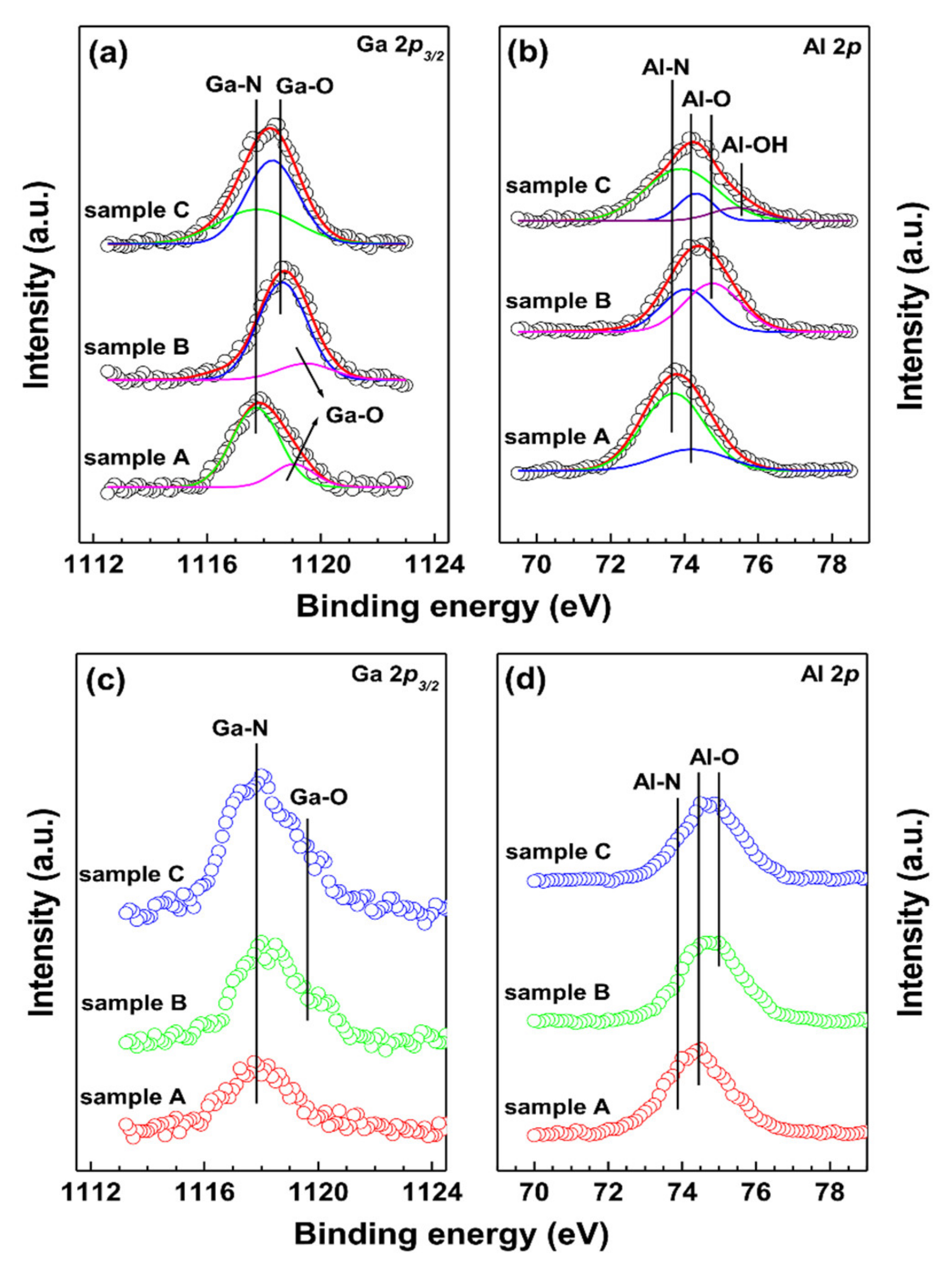
Figure 10a,b show the Ga 2p3/2 and Al 2p core level spectra, respectively, obtained from the AlGaN surface. The Ga 2p3/2 spectra showed the peaks associated with Ga–N from the AlGaN (~1117.8 eV [46]) and Ga–O (~1118.5 eV [46] and ~1119.2 eV [47]) from the surface. The integrated intensity ratios of [Ga–N]/[Ga–O] were calculated to be 4.04 and 0.62, for samples A and C, respectively. For sample B, the Ga–N peak was not observed clearly. The Al 2p spectra show the peaks consistent with Al–N bonding (at ~73.6 eV) and Al–O bonding (at ~74.5 eV) [46], with additional peaks at ~74.2 and ~75.6 eV related to AlOx and Al–OH, respectively [47]. Likewise, the integrated ratios of [Al–N]/[Al–O] were found to be 2.55, 0.12, and 2.34, for samples A, B, and C, respectively. These results indicate the clearer formation of the AlGaN layer and the presence of less oxygen-related bonding for sample A as compared with samples B and C. In addition, the incorporation of N atoms into the AlGaN layer occurred more effectively for sample A, related to the positive shift of flatband voltage. Figure 10c,d show the Ga 2p3/2 and Al 2p core level spectra, respectively, obtained from the AlGaN layer, where the etch depth was 5 nm. The integrated ratios of [Al–N]/[Al–O] were found to be 0.34, 0.03, and 0.17, for samples A, B, and C, respectively. Like the XPS spectra in Figure 10a,b, these also show that the oxygen-related bonding was formed more clearly for samples B and C. Therefore, the AlN and GaN pulse ratio of 2:1 could show less oxygen-related defects in the AlGaN layer. According to AES analysis, it was found that oxygen content reached 7 to 15 at.% in the AlGaN films grown on Si substrate. XPS analysis revealed that oxygen content in the AlGaN films on GaN substrate reached ~20 at.%. These values are higher than the value of 1.5–3 at.% in the plasma-assisted ALD-grown AlGaN film at 200 °C [18]. Oxygen could be incorporated from the surface oxidation when the film surface was exposed to air after the high temperature deposition process. In addition, water and oxygen gas molecules remain when the ALD chamber is open during loading/unloading the samples, and thus TMA could react with the remnant oxygen gas during the deposition process [48,49].
Generally, ALD-AlN films deposited at 350–425 °C using TMA and NH3 show high levels of carbon (4–8 at.%) and hydrogen (10–16 at.%) residues [50]. From XPS measurement, we observed that carbon content in the AlGaN film was below 1 at.%, meaning that carbon related impurities would be marginal. However, we could observe Al–OH bonding from the Al 2p core level spectra. Al–OH defects in ALD-Al2O3 films were associated with acceptor-like border traps and positive fixed charges in Al2O3 [51]. Hence, these Al–OH defects would affect the electrical properties in the AlGaN films. Meanwhile, hydrogen exposure at room temperature in Pt/SiO2/GaN diodes changed the conduction mechanisms from Fowler–Nordheim (FN) tunneling to PF emission and the C–V curve shifted toward negative bias values [52]. The significant increase in the capacitance at a low frequency in the Pt/AlGaN/GaN Schottky diodes was observed after hydrogen exposure, which was associated with hydrogen-related dipoles [53]. Hydrogen treatment on AlGaN/GaN HEMT was found to reduce the trap density by about one order of magnitude [54]. Hasegawa et al. observed a peak related with the N–Hx bond at ~399 eV in the N 1s core level spectrum of the H2 plasma-treated AlGaN/GaN, and they associated this with N vacancies and related defects near the AlGaN surface [55]. These results indicate that the exact role of hydrogen should be investigated to understand the nature of AlGaN/GaN-based devices.
On the basis of the results so far, we know that sample A would be the best material among the three samples because it revealed less oxygen-related defects and better interfacial quality. Thus, this condition would be used to grow AlGaN in HEMT devices. As already known, (Al)GaN epilayer grown by MOCVD or molecular beam epitaxy (MBE) is achieved at high temperatures. On the contrary, ALD grown (Al)GaN grown at low temperatures shows polycrystalline phases. This polycrystalline-(Al)GaN can be used instead of epi-(Al)GaN to obtain lower efficiency, but cost-effective devices. Hence, the application of ALD grown (Al)GaN can be widened further. Investigation with various pulse ratios of AlN and GaN is in progress to obtain the detailed properties of ALD grown AlGaN material.
4. Conclusions
We used ALD to grow AlGaN on n-GaN substrate with different pulse ratios of AlN and GaN and explored the current transport mechanisms and trapping properties of Pt/AlGaN/GaN Schottky diodes. At the low bias region, the sample with the pulse ratio of 2:1 was explained by Poole–Frenkel emission and the negative temperature dependence for the sample with the pulse ratio of 1:2 was associated with the acceptor levels in the AlGaN layer. According to the parallel conductance method, fast interface traps located at 0.24–0.29 eV were observed for the samples with the pulse ratios of 1:1 and 1:2. On the contrary, bulk traps at ~0.34 eV were observed for the sample with the pulse ratio of 2:1. C–V hysteresis measurements revealed the higher trap densities for the samples with the pulse ratios of 1:1 and 1:2, associated with the charge trapping in the interfacial oxide layer. Compared with other samples, the formation of oxidized transition layer near the AlGaN/GaN interface was suppressed for sample A.
Author Contributions
Conceptualization, H.K. and B.J.C.; methodology, H.K. and B.C.; investigation, H.K. and S.C.; writing—original draft, H.K.; writing—review and editing, H.K. and B.J.C. All authors have read and agreed to the published version of the manuscript.
Funding
This work was supported by Basic Science Research Program through the National Research Foundation of Korea (NRF) funded by the Ministry of Education (2017R1D1A1B03030400).
Conflicts of Interest
The authors declare no conflict of interest.
References
- Eastman, L.; Tilak, V.; Smart, J.; Green, B.; Chumbes, E.; Dimitrov, R.; Kim, H.; Ambacher, O.; Weimann, N.; Prunty, T.; et al. Undoped AlGaN/GaN HEMTs for microwave power amplification. IEEE Trans. Electron Dev. 2011, 48, 479–485. [Google Scholar] [CrossRef]
- Khandelwal, S.; Goyal, N.; Fjeldly, T. A physical-based analytical model for 2DEG charge density in AlGaN/GaN HEMT devices. IEEE Trans. Electron Dev. 2011, 58, 3622–3625. [Google Scholar] [CrossRef]
- Tan, W.; Uren, M.; Fry, P.; Houston, P.; Balmer, R.; Martin, T. High temperature performance of AlGaN/GaN HEMTs on Si substrates. Solid State Electron. 2006, 50, 511–513. [Google Scholar] [CrossRef]
- Wang, X.; Hu, G.; Ma, Z.; Ran, J.; Wang, C.; Xiao, H.; Tang, J.; Li, J.; Wang, J.; Zeng, Y.; et al. AlGaN/AlN/GaN/SiC HEMT structure with high mobility GaN thin layer as channel grown by MOCVD. J. Cryst. Growth 2007, 298, 835–839. [Google Scholar] [CrossRef]
- Higashiwaki, M.; Matsui, T.; Mimura, T. AlGaN/GaN MIS-HFETs with fT of 163 GHz using cat-CVD SiN gate-insulating and passivation layers. IEEE Electron Device Lett. 2006, 27, 6–18. [Google Scholar]
- Xia, L.; Hanson, A.; Boles, T.; Jin, D. On reverse gate leakage current of GaN high electron mobility transistors on silicon substrate. Appl. Phys. Lett. 2013, 102, 113510. [Google Scholar] [CrossRef]
- Turuvekere, S.; DasGupta, A.; DasGupta, N. Effect of barrier layer thickness on gate leakage current in AlGaN/GaN HEMTs. IEEE Trans. Electron Dev. 2015, 62, 3449–3452. [Google Scholar] [CrossRef]
- Swain, R.; Jena, K.; Lenka, T. Modeling of forward gate leakage current in MOSHEMT using trap-assisted tunneling and Poole-Frenkel emission. IEEE Trans. Electron Dev. 2012, 63, 2346–2352. [Google Scholar] [CrossRef]
- Fiorenza, P.; Greco, G.; Giannazzo, F.; Nigro, R.; Roccaforte, F. Poole-Frenkel emission in epitaxial nickel oxide on AlGaN/GaN heterostructures. Appl. Phys. Lett. 2012, 101, 172901. [Google Scholar] [CrossRef]
- Zhu, J.; Ma, X.; Hou, B.; Chen, W.; Hao, Y. Investigation of gate leakage mechanism in Al2O3/Al0.55Ga0.45N/GaN metal-oxide-semiconductor high-electron-mobility transistors. Appl. Phys. Lett. 2014, 104, 153510. [Google Scholar] [CrossRef]
- Liu, H.; Zhang, Z.; Luo, W. Analysis of reverse gate leakage mechanism of AlGaN/GaN HEMTs with N2 plasma surface treatment. Solid State Electron. 2018, 144, 60–66. [Google Scholar] [CrossRef]
- Xu, X.; Beling, C.; Fung, S.; Zhao, Y.; Sun, N.; Sun, T.; Zhang, Q.; Zhan, H.; Sun, B.; Wang, J.; et al. Formation mechanism of a degenerate thin layer at the interface of a GaN/sapphire system. Appl. Phys. Lett. 2000, 76, 152–154. [Google Scholar] [CrossRef] [Green Version]
- Ozgit, C.; Donmez, I.; Alevli, M.; Biyikli, N. Atomic layer deposition of GaN at low temperatures. J. Vac. Sci. Technol. A 2013, 30, 01A124. [Google Scholar] [CrossRef]
- Shih, H.; Lin, M.; Chen, L.; Chen, M. Uniform GaN thin films grown on (100) silicon by remote plasma atomic layer deposition. Nanotechnology 2015, 26, 014002. [Google Scholar] [CrossRef]
- Kim, H.; Kim, N.; An, S.; Yoon, H.; Choi, B. Improved interfacial properties of thermal atomic layer deposited AlN on GaN. Vacuum 2019, 159, 379–381. [Google Scholar] [CrossRef]
- Sadeghpour, S.; Ceyssens, F.; Puers, R. Crystalline growth of AlN thin films by atomic layer deposition. J. Phys. Conf. Ser. 2016, 757, 012003. [Google Scholar] [CrossRef]
- Rontu, V.; Sippola, P.; Broas, M.; Glenn, R.; Sajavaara, T.; Lipsanen, H.; Paulasto-Kröckel, M.; Franssila, S. Atomic layer deposition of AlN from AlCl3 using NH3 and Ar/NH3 plasma. J. Vac. Sci. Technol. A 2018, 36, 021508. [Google Scholar] [CrossRef] [Green Version]
- Ozgit-Akgun, C.; Goldenberg, E.; Okyay, A.; Biyikli, N. Hollow cathode plasma-assisted atomic layer deposition of crystalline AlN, GaN and AlxGa1−xN thin films at low temperatures. J. Mater. Chem. C 2014, 2, 2097–2284. [Google Scholar] [CrossRef] [Green Version]
- Kim, H.; Yun, H.; Choi, S.; Choi, B. Atomic layer deposition of AlGaN on GaN and current transport mechanism in AlGaN/GaN Schottky diodes. Mater. Trans. 2020, 61, 88–93. [Google Scholar] [CrossRef]
- Tung, R. Recent advances in Schottky barrier concepts. Mater. Sci. Eng. R 2001, 35, 1–138. [Google Scholar] [CrossRef]
- Zhang, H.; Miller, E.; Yu, E. Analysis of leakage current mechanisms in Schottky contacts to GaN and Al0.25Ga0.75N∕GaN grown by molecular-beam epitaxy. J. Appl. Phys. 2006, 99, 023703. [Google Scholar] [CrossRef] [Green Version]
- Persano, A.; Pio, I.; Tasco, V.; Cuscun, M.; Passaseo, A.; Cola, A. Electrical properties of planar AlGaN/GaN Schottky diodes: Role of 2DEG and analysis of non-idealities. J. Appl. Phys. 2017, 121, 135701. [Google Scholar] [CrossRef]
- Hierro, A.; Arehart, A.; Heying, B.; Hansen, M.; Mishra, U.; DenBaars, S.; Speck, J.; Ringel, S. Impact of Ga/N flux ratio on trap states in n-GaN n-GaN grown by plasma-assisted molecular-beam epitaxy. Appl. Phys. Lett. 2002, 80, 805–807. [Google Scholar] [CrossRef]
- Fang, Z.; Farlow, G.; Claflin, B.; Look, D.; Green, D. Effects of electron-irradiation on electrical properties of AlGaN/GaN Schottky barrier diodes. J. Appl. Phys. 2009, 105, 123704. [Google Scholar] [CrossRef] [Green Version]
- Liu, Z.; Ng, G.; Arulkumaran, S.; Maung, Y.; Zho, H. Temperature-dependent forward gate current transport in atomic-layer-deposited Al2O3/AlGaN/GaN metal-insulator-semiconductor high electron mobility transistor. Appl. Phys. Lett. 2011, 98, 163501. [Google Scholar] [CrossRef]
- Jos, R. Reverse Schottky gate current in AlGaN-GaN high-electron-mobility-transistors. J. Appl. Phys. 2012, 112, 094508. [Google Scholar] [CrossRef] [Green Version]
- Lu, X.; Liu, C.; Jiang, H.; Zou, X.; Zhang, A.; Lau, K. Ultralow reverse leakage current in AlGaN/GaN lateral Schottky barrier diodes grown on bulk GaN substrate. Appl. Phys. Exp. 2016, 9, 031001. [Google Scholar] [CrossRef] [Green Version]
- Saadaoui, S.; Salem, M.; Gassoumi, M.; Maaref, H.; Gaquière, C. Electrical characterization of (Ni/Au)/Al0.25Ga0.75N/GaN/SiC Schottky barrier diode. J. Appl. Phys. 2011, 110, 013701. [Google Scholar] [CrossRef]
- Weinstein, I.; Vokhmintsev, A.; Spiridonov, D. Thermoluminescence kinetics of oxygen-related centers in AlN single crystals. Diam. Relat. Mater. 2012, 25, 59. [Google Scholar] [CrossRef]
- Stampfl, C.; van de Walle, C. Theoretical investigation of native defects, impurities, and complexes in aluminum nitride. Phys. Rev. B 2002, 65, 1. [Google Scholar] [CrossRef] [Green Version]
- Tansley, T.; Egan, R. Point-defect energies in the nitrides of aluminum, gallium, and indium. Phys. Rev. B 1992, 45, 10942. [Google Scholar] [CrossRef] [PubMed]
- Sathaiya, D.; Karmalkar, S. Thermionic trap-assisted tunneling model and its application to leakage current in nitrided oxides and AlGaN∕GaN high electron mobility transistors. J. Appl. Phys. 2006, 99, 093701. [Google Scholar] [CrossRef]
- Liang, J.; Lai, L.; Zhou, Z.; Zhang, J.; Zhang, J.; Xu, J.; Zhang, Y.; Liu, X.; Luo, W. Trap-assisted tunneling current of ultrathin InAlN/GaN HEMTs on Si (1 1 1) substrate. Solid State Electron. 2019, 160, 107622. [Google Scholar] [CrossRef]
- Arulkumaran, S.; Egawa, T.; Ishikawa, H.; Jimbo, T. Temperature dependence of gate–leakage current in AlGaN/GaN high-electron-mobility transistors. Appl. Phys. Lett. 2013, 82, 3110–3112. [Google Scholar] [CrossRef]
- Suemitsu, T.; Tomizawa, M.; Enoki, T.; Ishii, Y. Enhancement of weak impact ionization in InAlAs/InGaAs HEMTs induced by surface traps: Simulation and experiments, IWCE-6, Computational Electronics. In Extended Abstracts of 1998 Sixth International Workshop; IEEE: Piscataway, NJ, USA, 1998; pp. 250–253. [Google Scholar]
- Arulkumaran, S.; Egawa, T.; Ishikawa, H. Studies on the influences of i-GaN, n-GaN, p-GaN and InGaN cap layers in AlGaN/GaN high-electron-mobility transistors. Jpn. J. Appl. Phys. 2005, 44, 2953–2960. [Google Scholar] [CrossRef]
- Srivastava, S.; Hwang, S.; Islam, M.; Balakrishnan, K.; Adivarahan, V.; Khan, A. Ohmic contact to high-aluminum-content AlGaN epilayers. J. Electron. Mater. 2009, 38, 2348. [Google Scholar] [CrossRef]
- Ambacher, O.; Smart, J.; Shealy, J.; Weimann, N.; Chu, K.; Murphy, M.; Schaff, W.; Eastman, L.; Dimitrov, R.; Wittmer, L.; et al. Two-dimensional electron gases induced by spontaneous and piezoelectric polarization charges in N- and Ga-face AlGaN/GaN heterostructures. J. Appl. Phys. 1999, 85, 3222–3233. [Google Scholar] [CrossRef] [Green Version]
- Silvestri, M.; Uren, M.; Kuball, M. Iron-induced deep-level acceptor center in GaN/AlGaN high electron mobility transistors: Energy level and cross section. Appl. Phys. Lett. 2013, 102, 073501. [Google Scholar] [CrossRef] [Green Version]
- Ma, X.; Zhu, J.; Liao, X.; Yue, T.; Chen, W.; Hao, Y. Quantitative characterization of interface traps in Al2O3/AlGaN/GaN metal-oxide-semiconductor high-electron-mobility transistors by dynamic capacitance dispersion technique. Appl. Phys. Lett. 2013, 103, 033510. [Google Scholar] [CrossRef]
- Zeng, H.; Hao, L.; Luo, W.; Liao, X.; Huang, W.; Lin, Y.; Li, Y. Trapping properties of LiNbO3/AlGaN/GaN metal-ferroelectric-semiconductor heterostructure characterized by temperature dependent conductance measurements. J. Appl. Phys. 2010, 107, 084508. [Google Scholar] [CrossRef]
- Kordoš, P.; Stoklas, R.; Gregušová, D.; Novák, J. Characterization of AlGaN/GaN metal-oxide-semiconductor field-effect transistors by frequency dependent conductance analysis. Appl. Phys. Lett. 2009, 94, 223512. [Google Scholar] [CrossRef]
- Lin, J.; Gomeniuk, Y.; Monaghan, S.; Povey, I.; Cherkaoui, K.; O’Connor, E.; Power, M.; Hurley, P. An investigation of capacitance-voltage hysteresis in metal/high-k/In0.53Ga0.47As metal-oxide-semiconductor capacitors. J. Appl. Phys. 2013, 114, 144105. [Google Scholar] [CrossRef] [Green Version]
- Sang, L.; Ren, B.; Liao, M.; Koide, Y.; Sumiya, M. Suppression in the electrical hysteresis by using CaF2 dielectric layer for p-GaN MIS capacitors. J. Appl. Phys. 2018, 123, 161423. [Google Scholar] [CrossRef]
- Kim, H.; Kwon, Y.; Choi, B. AlN passivation effect on Au/GaN Schottky contacts. Thin Solid Film. 2019, 670, 41–45. [Google Scholar] [CrossRef]
- Qin, X.; Dong, H.; Kim, J.; Wallace, R. A crystalline oxide passivation for Al2O3/AlGaN/GaN. Appl. Phys. Lett. 2014, 105, 141604. [Google Scholar] [CrossRef] [Green Version]
- Kim, H.; Yoon, H.; Choi, B. Thickness dependence on interfacial and electrical properties in atomic layer deposited AlN on c-plane GaN. Nanoscale Res. Lett. 2008, 13, 232. [Google Scholar] [CrossRef] [Green Version]
- Bosund, M.; Sajavaara, T.; Laitinen, M.; Huhtio, T.; Putkonen, M.; Airaksinen, V.; Lipsanen, H. Properties of AlN grown by plasma enhanced atomic layer deposition. Appl. Surf. Sci. 2011, 257, 7827–7830. [Google Scholar] [CrossRef]
- Nguyen, H.; Tang, H.; Huang, W.; Lin, M. Mechanisms for reactions of trimethylaluminum with molecular oxygen and water. Comput. Theor. Chem. 2014, 1035, 39–43. [Google Scholar] [CrossRef]
- Lee, Y.; Kang, S. Growth of aluminum nitride thin films prepared by plasma-enhanced atomic layer deposition. Thin Solid Film. 2004, 446, 227. [Google Scholar] [CrossRef]
- Raja, L.; Nguyen, C.; Lee, C.; Balaji, N.; Chatterjee, S.; Jang, K.; Kim, H.; Yi, J. Improved data retention of InSnZnO nonvolatile memory by H2O2 treated Al2O3 tunneling layer: A cost-effective method. IEEE Electron Dev. Lett. 2016, 37, 1272. [Google Scholar] [CrossRef]
- Irokawa, Y. Hydrogen-induced change in the electrical properties of metal-insulator-semiconductor Pt–GaN diodes. J. Appl. Phys. 2010, 108, 094501. [Google Scholar] [CrossRef]
- Irokawa, Y.; Matsuki, N.; Sumiya, M.; Sakuma, Y.; Sekiguchi, T.; Chikyo, T.; Sumida, Y.; Nakano, Y. Anomalous capacitance-voltage characteristics of Pt-AlGaN/GaN Schottky diodes exposed to hydrogen. Phys. Status Solidi C 2010, 7, 1928. [Google Scholar] [CrossRef]
- Chen, Y.; Zhang, Y.; Liu, Y.; Liao, X.; En, Y.; Fang, W.; Huang, Y. Effect of hydrogen on defects of AlGaN/GaN HEMTs characterized by low-frequency noise. IEEE Trans. Electron Dev. 2018, 65, 1321. [Google Scholar] [CrossRef]
- Hasegawa, H.; Inagaki, T.; Ootomo, S.; Hashizume, T. Mechanisms of current collapse and gate leakage currents in AlGaN/GaN heterostructure field effect transistors. J. Vac. Sci. Technol. B 2013, 21, 1844. [Google Scholar] [CrossRef] [Green Version]
Figure 1.
(a) Schematic layer structures of AlGaN/GaN devices and prepared AlGaN layers with different pulse ratios. (b–d) The atomic force microscopy (AFM) surface images scanned over 2 μm × 2 μm areas.
Figure 1.
(a) Schematic layer structures of AlGaN/GaN devices and prepared AlGaN layers with different pulse ratios. (b–d) The atomic force microscopy (AFM) surface images scanned over 2 μm × 2 μm areas.

Figure 2.
Semilogarithmic current–voltage (I–V) data obtained at different temperatures for samples (a) A, (b) B, and (c) C. The inset in (c) shows the I–V curves for narrow forward bias range obtained from sample C.
Figure 2.
Semilogarithmic current–voltage (I–V) data obtained at different temperatures for samples (a) A, (b) B, and (c) C. The inset in (c) shows the I–V curves for narrow forward bias range obtained from sample C.

Figure 3.
(a) Barrier height and (b) ideality factor at different temperatures.

Figure 4.
(a) Ln(J/E) vs. E1/2/plots by the Poole–Frenkel (PF) emission model, together with the linear fitting to the experimental data for sample A. (b,c) The calculated m and b values, respectively.
Figure 4.
(a) Ln(J/E) vs. E1/2/plots by the Poole–Frenkel (PF) emission model, together with the linear fitting to the experimental data for sample A. (b,c) The calculated m and b values, respectively.

Figure 5.
(a) Trap assisted tunneling (TAT) plots of ln(J) vs. 1/E and (b) the obtained trap energy for sample A.
Figure 5.
(a) Trap assisted tunneling (TAT) plots of ln(J) vs. 1/E and (b) the obtained trap energy for sample A.

Figure 6.
(a) Trap assisted tunneling (TAT) plots of ln(J) vs. 1/E and (b) the obtained trap energy for sample B.
Figure 6.
(a) Trap assisted tunneling (TAT) plots of ln(J) vs. 1/E and (b) the obtained trap energy for sample B.

Figure 7.
Reverse leakage current density vs. temperature at different reverse biases for samples (a) A and (b) C. The insets in (a) and (b) show the obtained activation energies for samples A and C, respectively.
Figure 7.
Reverse leakage current density vs. temperature at different reverse biases for samples (a) A and (b) C. The insets in (a) and (b) show the obtained activation energies for samples A and C, respectively.

Figure 8.
Capacitance–voltage (C–V) data at different frequencies for samples (a) A, (b) B, and (c) C, and frequency-dependent parallel conductance–voltage (Gp/ω–V) curves for samples (d) A, (e) B, and (f) C.
Figure 8.
Capacitance–voltage (C–V) data at different frequencies for samples (a) A, (b) B, and (c) C, and frequency-dependent parallel conductance–voltage (Gp/ω–V) curves for samples (d) A, (e) B, and (f) C.

Figure 9.
(a) Trap density vs. energy level, (b) time constant vs. voltage, (c) C–V hysteresis plots obtained at 100 kHz, and (d) cross-sectional scanning transmission electron microscopy (STEM) image for sample B.
Figure 9.
(a) Trap density vs. energy level, (b) time constant vs. voltage, (c) C–V hysteresis plots obtained at 100 kHz, and (d) cross-sectional scanning transmission electron microscopy (STEM) image for sample B.

Figure 10.
X-ray photoelectron spectroscopy (XPS) core level spectra of (a) Ga 3p/3/2 and (b) Al 2p from the AlGaN surface, and (c) Ga 3p/3/2 and (d) Al 2p from the AlGaN layer where the etch depth is 5 nm.
Figure 10.
X-ray photoelectron spectroscopy (XPS) core level spectra of (a) Ga 3p/3/2 and (b) Al 2p from the AlGaN surface, and (c) Ga 3p/3/2 and (d) Al 2p from the AlGaN layer where the etch depth is 5 nm.

© 2020 by the authors. Licensee MDPI, Basel, Switzerland. This article is an open access article distributed under the terms and conditions of the Creative Commons Attribution (CC BY) license (http://creativecommons.org/licenses/by/4.0/).
Share and Cite
MDPI and ACS Style
Kim, H.; Choi, S.; Choi, B.J. Influence of AlN and GaN Pulse Ratios in Thermal Atomic Layer Deposited AlGaN on the Electrical Properties of AlGaN/GaN Schottky Diodes. Coatings 2020, 10, 489. https://doi.org/10.3390/coatings10050489
AMA Style
Kim H, Choi S, Choi BJ. Influence of AlN and GaN Pulse Ratios in Thermal Atomic Layer Deposited AlGaN on the Electrical Properties of AlGaN/GaN Schottky Diodes. Coatings. 2020; 10(5):489. https://doi.org/10.3390/coatings10050489
Chicago/Turabian StyleKim, Hogyoung, Seok Choi, and Byung Joon Choi. 2020. "Influence of AlN and GaN Pulse Ratios in Thermal Atomic Layer Deposited AlGaN on the Electrical Properties of AlGaN/GaN Schottky Diodes" Coatings 10, no. 5: 489. https://doi.org/10.3390/coatings10050489
Note that from the first issue of 2016, this journal uses article numbers instead of page numbers. See further details here.