Low-Loss and Broadband Silicon Photonic 3-dB Power Splitter with Enhanced Coupling of Shallow-Etched Rib Waveguides


School of Electrical Engineering and Computer Science, Gwangju Institute of Science and Technology, Gwangju 61005, Korea
*
Author to whom correspondence should be addressed.
Appl. Sci. 2020, 10(13), 4507; https://doi.org/10.3390/app10134507
Submission received: 10 June 2020
/
Revised: 24 June 2020
/
Accepted: 25 June 2020
/
Published: 29 June 2020
(This article belongs to the Collection New Trends in Optical Networks)
Abstract
:Featured Application
Silicon photonics, High-density integrated photonic devices, Photonic switches, 1 × N power splitters.
Abstract
A silicon photonic 3-dB power splitter is one of the essential components to demonstrate large-scale silicon photonic integrated circuits (PICs), and can be utilized to implement modulators, 1 × 2 switches, and 1 × N power splitters for various PIC applications. In this paper, we reported the design and experimental demonstration of low-loss and broadband silicon photonic 3-dB power splitters. The power splitter was realized by adiabatically tapered rib waveguides with 60-nm shallow etches. The shallow-etched rib waveguides offered strong coupling and relaxed critical dimensions (a taper tip width of 200 nm and gap spacing of 300 nm). The fabricated device exhibited an excess loss as low as 0.06 dB at a 1550-nm wavelength and a broad operating wavelength range from 1470 nm to 1570 nm. The relaxed critical dimensions (≥200 nm) make the power splitter compatible with standard fabrication processes of existing silicon photonics foundries.
1. Introduction
Silicon photonics has emerged as a powerful technology for optical networks in datacom and computercom with the commercial success of silicon photonic transceivers [1,2,3]. In the past decade, silicon photonics has been rapidly matured with the process standardization and the process design kit (PDK) development of silicon photonic foundries [4,5]. Large-scale silicon photonic integrated circuits have been demonstrated for a variety of applications, such as photonic switches [6,7,8], optical phased arrays (OPAs) [9,10,11,12], and programmable photonic processors [13,14,15,16,17]. A 3-dB optical power splitter is one of the key components to build high-density integrated photonic devices with multi-channel and parallel processing. A 3-dB optical power splitter can be employed in integrated Mach-Zehnder interferometers (MZI) to demonstrate intensity modulators or 1 × 2 switches [18,19,20], where the light traveling in a waveguide is split into two arms, the sensing and the reference arms. The optical power uniformity between two arms is extremely significant, which has motivated us to design a compact, low-loss, and excellent power uniformity optical power splitter. The 3-dB power splitters can be also utilized to demonstrate 1 × N splitters [9,12,21,22]. Notably, low-loss and uniform 1 × N power splitters are essential devices for large-scale silicon photonic OPAs. Various silicon photonic 3-dB power splitters have been demonstrated with multimode interferometers [9,12,22,23,24], directional couplers (DCs) [25], asymmetric waveguide-based phase control [26], adiabatic couplers with S-bend based Y-branches [27], and parameterized Y-junctions [28], which typically exhibit non-negligible excess losses or limited bandwidths.
Recently, low-loss and broadband power splitters based on adiabatically tapered waveguides have been reported [29,30]. However, these power splitters were designed with silicon strip waveguides, which cause tight mode confinement and weak coupling strength between waveguides. As a result, the designed critical dimensions (CDs) such as tapered tips and waveguide-gaps (30~50 nm), are beyond the deep ultraviolet (DUV) lithography limit of typical silicon photonics foundries. In this paper, we reported the experimental demonstration of power splitters based on adiabatically tapered silicon rib waveguides. The shallow-etched rib waveguides offered relatively strong coupling and relaxed critical dimensions (CDs ≥ 200 nm), which allowed the device dimensions to be compatible with standard processes of existing silicon photonic foundries. The demonstrated device had a low excess loss of 0.06 dB and a wide operating wavelength range over 100 nm (1470~1570 nm). The fabrication tolerance analysis confirmed that the proposed power splitter is fabrication insensitive within a large deviation range of ±50 nm for both the width and gap.
2. Device Design
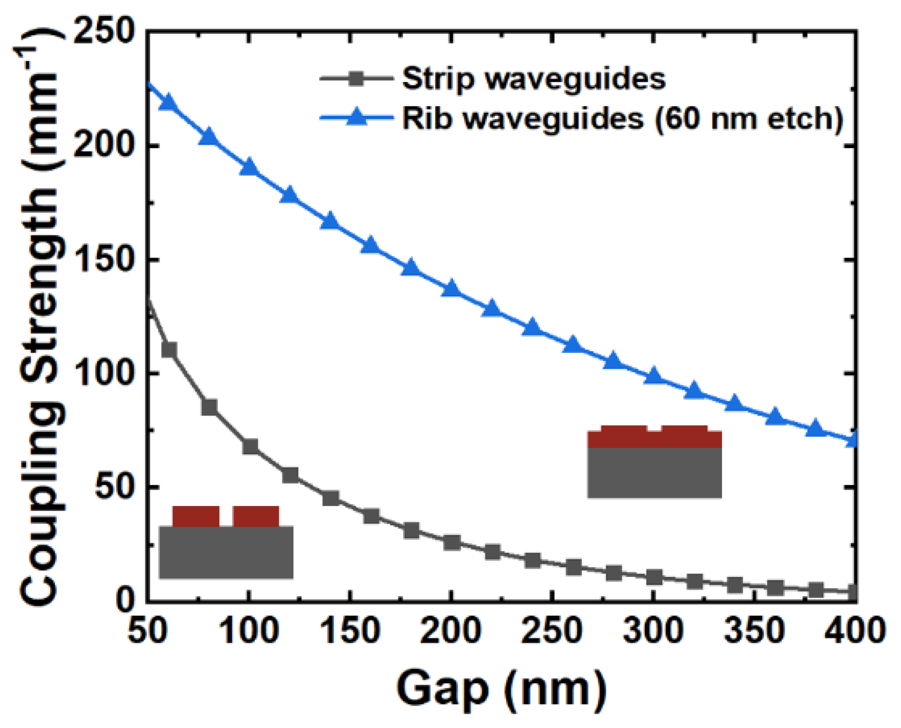
As the proposed power splitter is based on the adiabatic coupling of tapered waveguides, the coupling strength of the waveguides is a key parameter to achieve a compact device design. The strong coupling can readily be obtained by reducing the gap spacing between the waveguides. However, small gap spacing beyond the lithography limit prohibits a wide spread of applications of the device. An alternative way to achieve strong coupling is to utilize shallow-etched rib waveguides for enhanced mode overlap. Figure 1 shows the coupling strength of two identical waveguides for different waveguide types: (1) Silicon strip waveguides and (2) silicon rib waveguides. The thickness and width of the waveguides were chosen to be 220 nm and 500 nm, which well supported the single TE0 mode for both types of waveguides. The partial etch depth of the rib waveguide was 60 nm. The result clearly shows that the rib waveguides had stronger couplings than the strip waveguides. The gap spacing dimension can be relaxed for the rib coupled-waveguide. Therefore, we chose rib waveguides for our power splitter design to achieve DUV lithography-compatible CDs. Shallow-etched waveguides also provided low propagation loss, owing to the small mode overlap with the sidewall roughness.
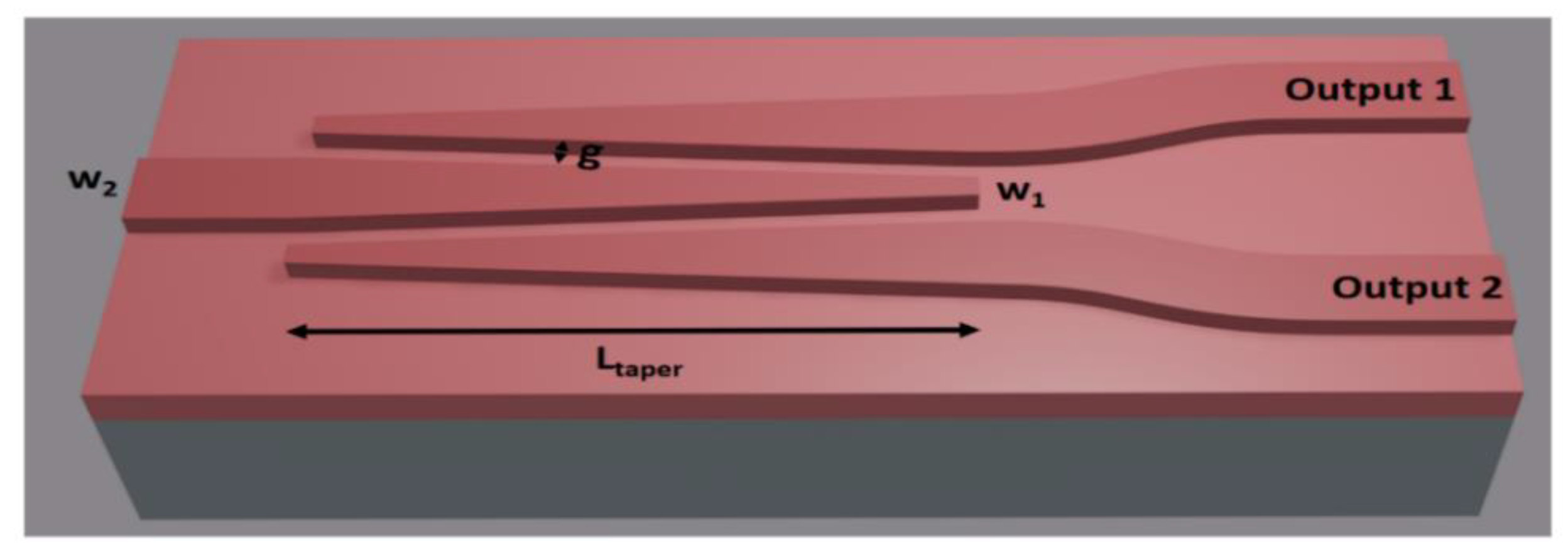
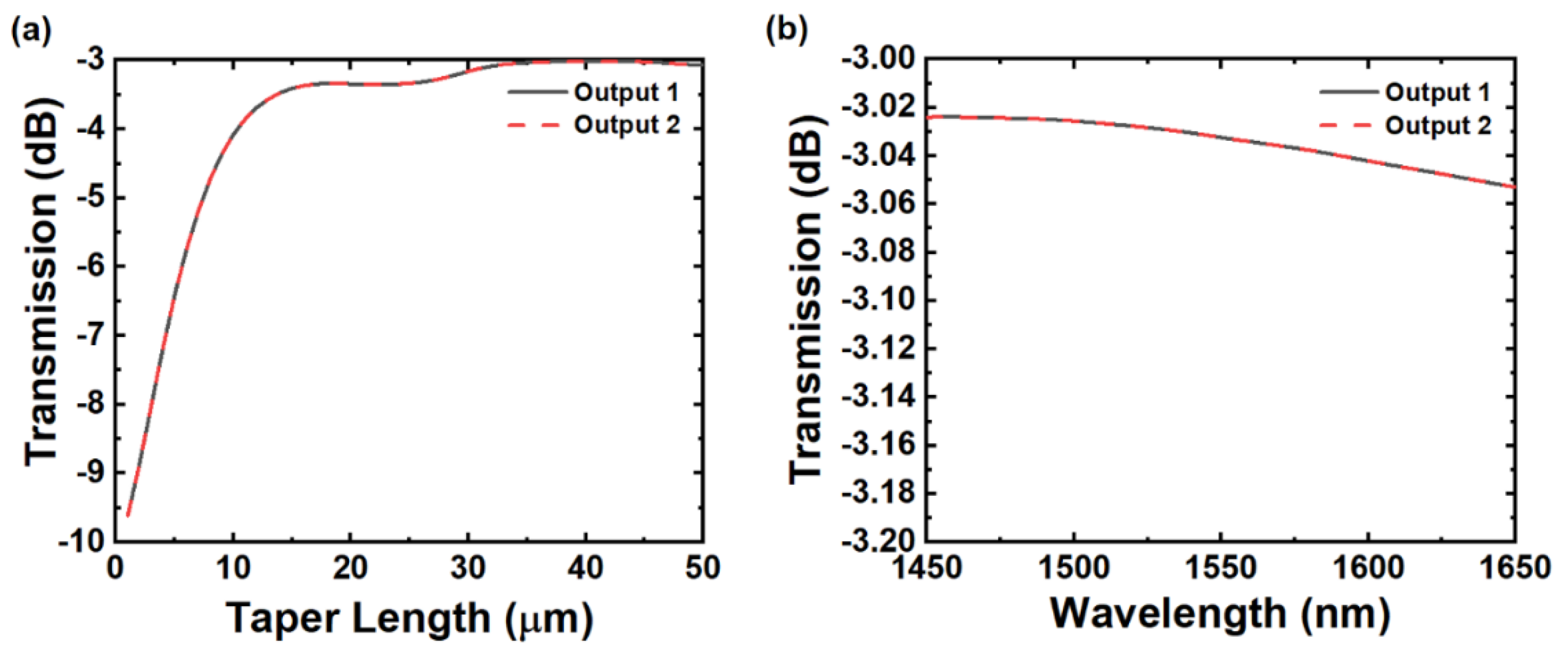
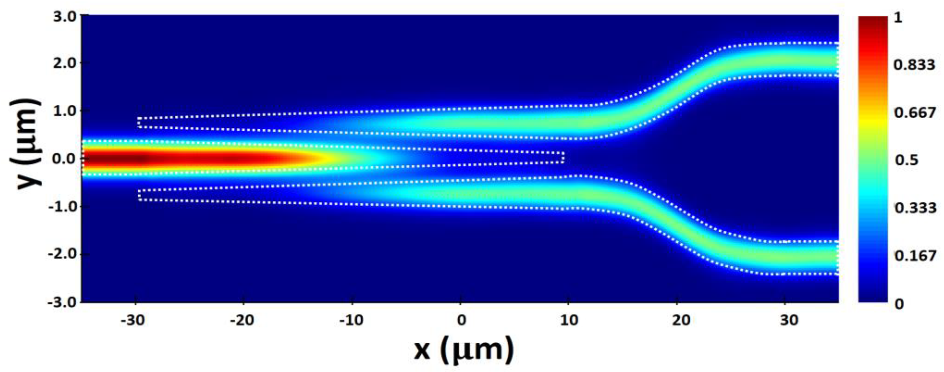
Figure 2 shows the schematic of the proposed 3-dB power splitter, consisting of one input waveguide and two output waveguides. A 2-μm-thick buried oxide (BOX) layer (n = 1.444 at 1550 nm) is in grey. The silicon rib waveguides (n = 3.476 at 1550 nm), with a thickness of 220 nm and a partial etch depth of 60 nm, are in red. The input waveguide and the two output waveguides had identical dimensions. Using eigenmode expansion (EME) solver, the device design was optimized. The waveguides were linearly tapered from the tip width (w1) of 200 nm to the waveguide width (w2) of 700 nm. The gap spacing between waveguides was designed to be 300 nm. In order to design the taper length, we investigated the transmission with the taper length sweep, as shown in Figure 3a. The taper length was chosen to be 40 µm, at which the transmission converged to −3.03 dB. Although our current design employed the linear taper, the taper length can be significantly reduced by utilizing the optimal curvature of the taper [31]. The spectral responses of the designed device were also simulated using the FDTD (Finite-Difference Time-Domain) solver. Thanks to the adiabatically tapered waveguides, the broad operation bandwidth over the 200-nm wavelength range was confirmed, as shown in Figure 3b. The normalized E-field intensity profile of the device is presented in Figure 4, which confirms symmetric 3-dB power splitting characteristic.
3. Experimental Results
The silicon photonic 3-dB power splitters were fabricated in an 8-inch wafer-scale silicon process facility using deep-UV (DUV) lithography. The designed power splitters were implemented on an 8-inch silicon-on-insulator (SOI) wafer with a 220-nm-thick device layer and a 2-μm-thick buried oxide (BOX) layer. First, we deposited a 70-nm-thick layer of Tetraethyl Orthosilicate (TEOS) by low-pressure chemical vapor deposition (LPCVD) as a hard mask layer. Then, we deposited patterned rib waveguides with DUV lithography, and a 60-nm-deep shallow etch on the silicon device layer. Strip waveguides were also implemented by subsequent DUV lithography and silicon full etch. Finally, the remaining oxide hard mask layer was removed by wet etching.
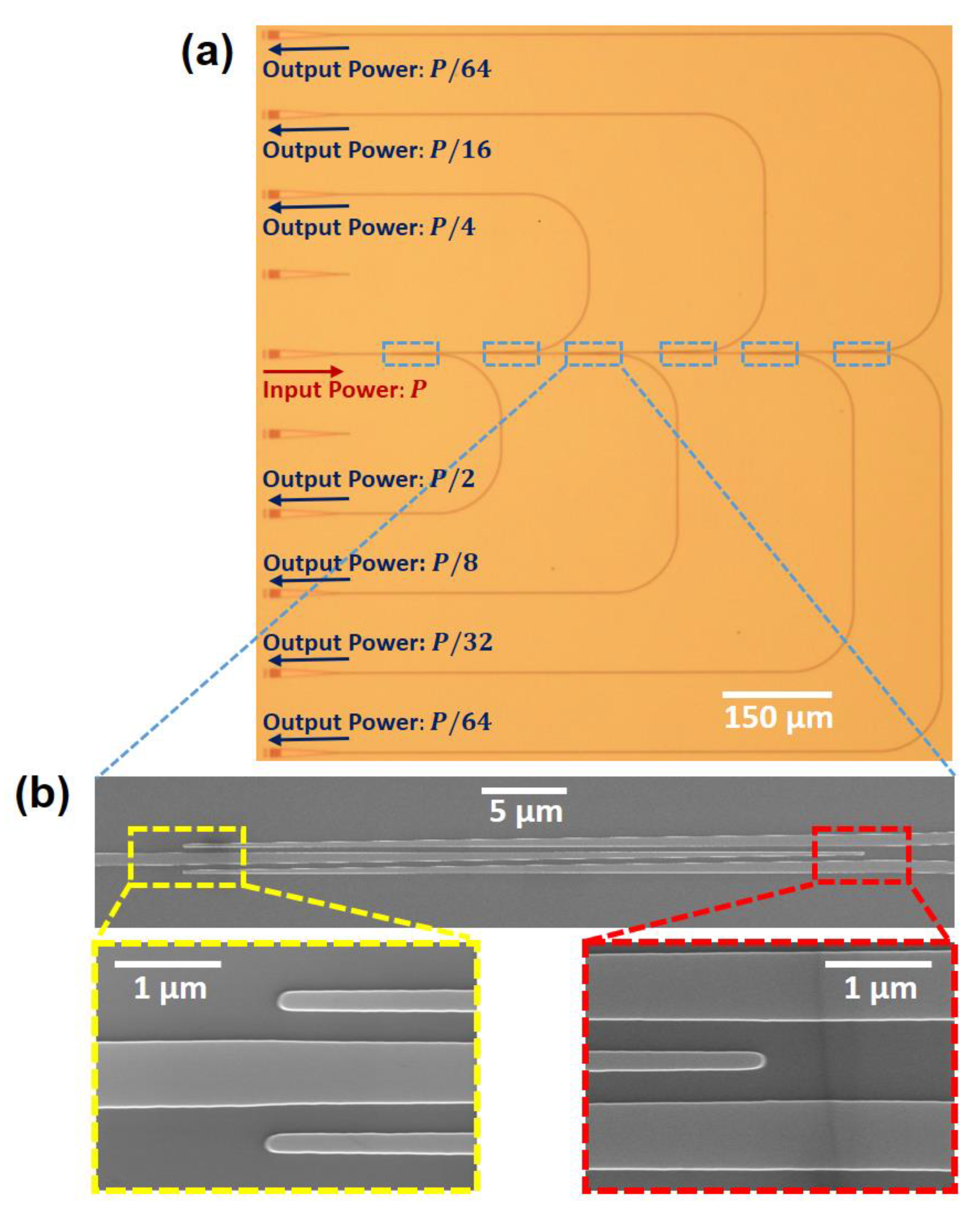
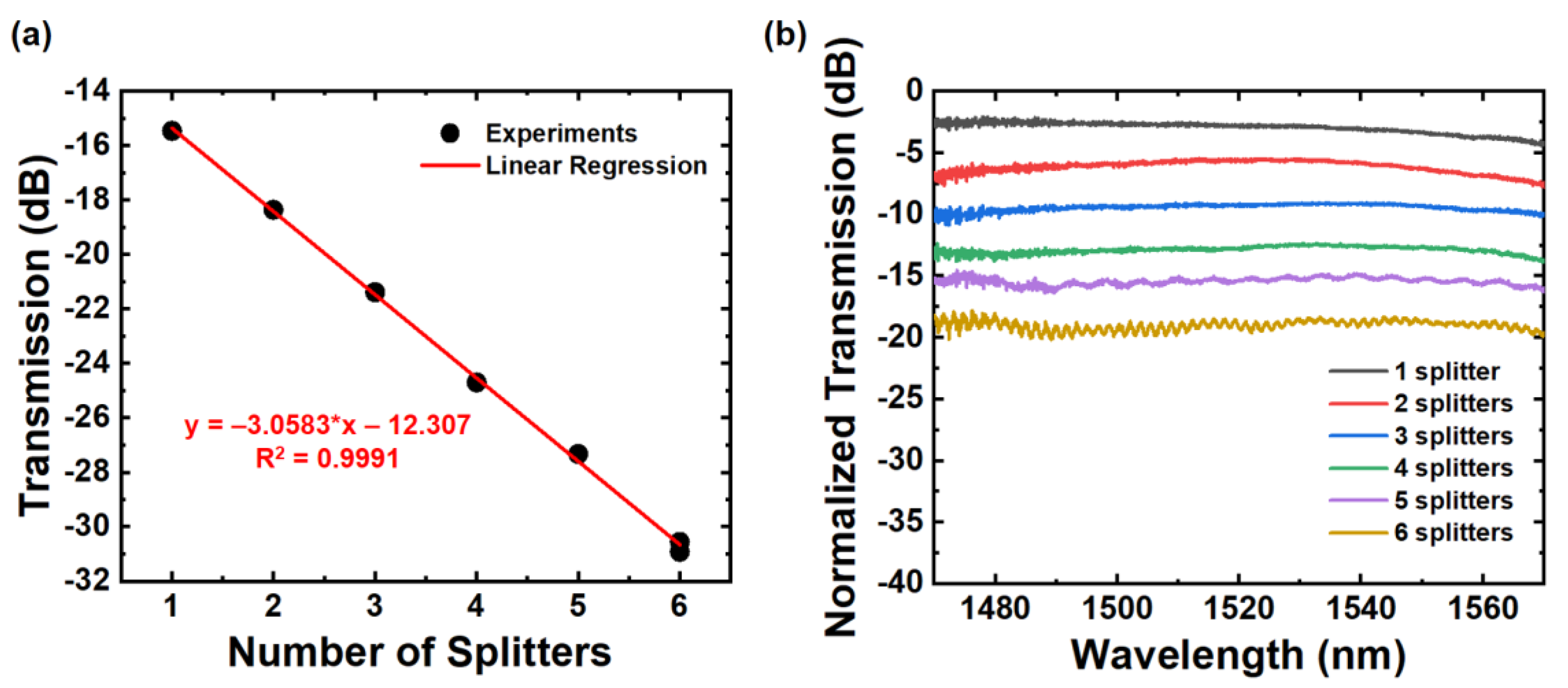
In order to characterize the fabricated power splitter, we used cascaded six stages of the 1 × 2 3-dB power splitter, as shown in Figure 5a. We employed vertical grating couplers to couple light into the fabricated device. The coupling loss of the grating couplers was measured to be ~6.0 dB from a back-to-back grating coupler pair on the same chip. The input power is P, and the cascaded output powers were then P/2, P/4, P/8, P/16, P/32, and P/64, respectively, as indicated in the Figure 5a. Figure 5b shows the scanning electron microscope (SEM) images of the fabricated power splitter, which confirm a good agreement with the device design. The nominal waveguide width and gap were observed to be 740 nm and 340 nm. The fabrication deviation from the design was below 50 nm. For the experimental characterization, we used a linear array of polarization-maintaining (PM) fibers with 127-μm pitch to guarantee consistent coupling losses from optical ports of the cascaded power splitters. TE-polarized light was coupled to the fabricated device through grating coupler array. The transmission of each stage was measured at the wavelength of 1550 nm and plotted as a function of the number of splitters, as shown in Figure 6a. The transmission of the single power splitter was measured to be −3.06 dB from the linear regression. The excess loss was estimated to be 0.06 dB (= 3.06 dB − 3 dB). The spectral response of each stage is shown in Figure 6b, exhibiting the broad operating bandwidth over the wavelength range of 100 nm from 1470 nm to 1570 nm. The transmission of each stage (one splitter, two splitters, etc.) was normalized to the transmission of a back-to-back grating coupler pair.
4. Discussion
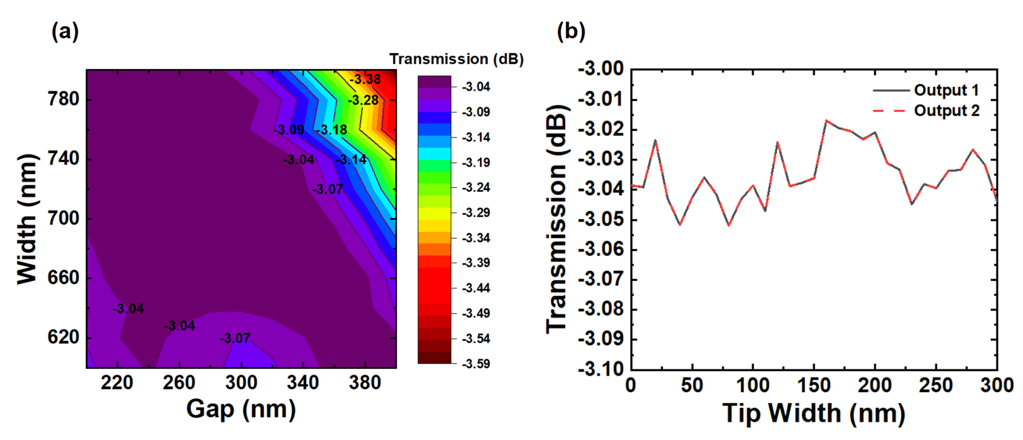
The strong coupling of the rib waveguides enabled the device design with large CD (200 nm), which was compatible with typical existing silicon photonics foundries. It was noted that the top oxide cladding could be added without significant changes in the device’s performance. We also investigated the fabrication tolerance of the device using EME simulations. Figure 7a shows the calculated transmissions of the power splitter with the deviations of the waveguide width and the gap from the optimum designs, confirming good fabrication tolerance of our power splitter design. The calculated excess loss of the device exhibited an excess loss as low as 0.07 dB, even with considerable fabrication variations (dark and light purple regions). For example, the excess loss of the power splitter can be below 0.07 dB as long as the waveguide width and gap are controlled within the fabrication variations of ±50 nm, which can be readily achieved from commercial silicon photonics foundries. For our fabricated device (the corresponding dimensions for waveguide width and gap spacing of 740 nm and 340 nm, respectively), the excess loss was expected to be lower than 0.07 dB. Our measured excess loss of 0.06 dB agrees well with this fabrication tolerance study. In addition, the tolerance simulation for the tip width was also performed. The excess loss was below 0.05 dB as long as the tip width was controlled to be smaller than 300 nm, as shown in Figure 7b.
Table 1 shows the summary of previously reported experimental power splitters and this work. Power splitters based on adiabatically tapered waveguides exhibited relatively low excess losses compared to other types. Whereas adiabatic power splitters with strip waveguides suffered from their small CDs, adiabatic power splitters with shallow-etched rib waveguides are promising in large-scale integrated photonic devices, considering their low loss (0.06 dB) and relaxed CD (200 nm), which are compatible with typical existing silicon photonics foundries.
5. Conclusions
We demonstrated low loss, broadband, and fabrication-insensitive silicon photonic 3-dB power splitters based on adiabatically tapered rib waveguide. The shallow-etched rib waveguides were employed to make the critical dimensions of the designed device larger than 200 nm. The compact power splitter with the taper length of 40 µm exhibited a low excess loss of 0.06 dB and a broad bandwidth over a 100-nm wavelength. The design compatibility with existing silicon photonics foundries and good fabrication tolerance enable the wide usage of the power splitter on a variety of silicon photonics applications. Thanks to its low loss, the proposed power splitter can favorably be integrated to demonstrate large-scale photonic integrated circuits.
Author Contributions
Design, V.H.N.; Simulation and Layout, V.H.N. and I.K.K.; writing—original draft preparation, V.H.N.; writing—review and editing, V.H.N. and T.J.S.; supervision, T.J.S. All authors have read and agreed to the published version of the manuscript.
Funding
This research was supported by National Research Foundation of Korea (NRF) grant funded by the Korean government (MSIT) (No. 2018R1C1B6005302); Nano·Material Technology Development Program through the National Research Foundation of Korea (NRF) funded by the Ministry of Science, ICT and Future Planning. (2009-0082580); GIST Research Institute (GRI) grant funded by the GIST in 2020.
Acknowledgments
The authors would like to thank Jong-Bum You for discussion on the fabrication process at NNFC.
Conflicts of Interest
The authors declare no conflict of interest.
References
- Wang, H.; Chai, H.; Lv, Z.; Zhang, Z.; Meng, L.; Yang, X.; Yang, T. Silicon photonic transceivers for application in data centers. J. Semicond. 2020, 41, 1–16. [Google Scholar]
- Abrams, N.; Cheng, Q.; Glick, M.; Jezzini, M.A.; Morrissey, P.E.; O’brien, P.; Bergman, K. Silicon Photonic 2.5D Multi-Chip Module Transceiver for High-Performance Data Centers. J. Lightwave Technol. 2020. [Google Scholar] [CrossRef]
- Pasricha, S.; Nikdast, M. A Survey of Silicon Photonics for Energy Efficient Manycore Computing. IEEE Des. Test 2020. [Google Scholar] [CrossRef]
- Thomson, D.; Zilkie, A.; Bowers, J.E.; Komljenovic, T.; Reed, G.T.; Vivien, L.; Marris-Morini, D.; Cassan, E.; Virot, L.; Fédéli, J.-M.; et al. Roadmap on silicon photonics. J. Opt. 2016, 18, 073003. [Google Scholar] [CrossRef]
- Chen, H.; Zhang, Z.; Huang, B.; Mao, L.; Zhang, Z. Progress in complementary metal-oxide-semiconductor silicon photonics and optoelectronic integrated circuits. J. Semicond. 2015, 36, 121001. [Google Scholar] [CrossRef]
- Tu, X.; Song, C.; Huang, T.; Chen, Z.; Fu, H. State of the Art and Perspectives on Silicon Photonic Switches. Micromachines 2019, 10, 51. [Google Scholar] [CrossRef] [Green Version]
- Seok, T.J.; Kwon, K.; Henriksson, J.; Luo, J.; Wu, M.C. Wafer-scale silicon photonic switches beyond die size limit. Optica 2019, 6, 490. [Google Scholar] [CrossRef]
- Dumais, P.; Goodwill, D.J.; Celo, D.; Jiang, J.; Zhang, C.; Zhao, F.; Tu, X.; Zhang, C.; Yan, S.; He, J.; et al. Silicon Photonic Switch Subsystem with 900 Monolithically Integrated Calibration Photodiodes and 64-Fiber Package. J. Lightwave Technol. 2018, 36, 233–238. [Google Scholar] [CrossRef]
- Kim, S.-H.; You, J.-B.; Ha, Y.-G.; Kang, G.; Lee, D.-S.; Yoon, H.; Yoo, D.-E.; Lee, D.-W.; Yu, K.; Youn, C.-H.; et al. Thermo-optic control of the longitudinal radiation angle in a silicon-based optical phased array. Opt. Lett. 2019, 44, 411. [Google Scholar] [CrossRef]
- Chung, S.; Abediasl, H.; Hashemi, H. A Monolithically Integrated Large-Scale Optical Phased Array in Silicon-on-Insulator CMOS. IEEE J. Solid State Circuits 2018, 53, 275–296. [Google Scholar] [CrossRef]
- Sun, J.; Timurdogan, E.; Yaacobi, A.; Su, Z.; Hosseini, E.S.; Cole, D.B.; Watts, M.R. Large-Scale Silicon Photonic Circuits for Optical Phased Arrays. IEEE J. Sel. Top. Quantum Electron. 2014, 20, 264–278. [Google Scholar] [CrossRef]
- Acoleyen, K.V.; Bogaerts, W.; Jágerská, J.; Thomas, N.L.; Houdré, R.; Baets, R. Off-chip beam steering with a one-dimensional optical phased array on silicon-on-insulator. Opt. Lett. 2009, 34, 1477–1479. [Google Scholar] [CrossRef] [PubMed]
- Teng, M.; Fathpour, S.; Safian, R.; Zhuang, L.; Honardoost, A.; Alahmadi, Y.; Polkoo, S.S.; Kojima, K.; Wen, H.; Renshaw, C.K.; et al. Miniaturized Silicon Photonics Devices for Integrated Optical Signal Processors. J. Lightwave Technol. 2020, 38, 6–17. [Google Scholar] [CrossRef]
- Zhou, H.; Zhao, Y.; Wei, Y.; Li, F.; Dong, J.; Zhang, X. All-in-one silicon photonic polarization processor. Nanophotonics 2019, 8, 2257–2267. [Google Scholar] [CrossRef]
- Harris, N.C.; Carolan, J.; Bunandar, D.; Prabhu, M.; Hochberg, M.; Baehr-Jones, T.; Fanto, M.L.; Smith, A.M.; Tison, C.C.; Alsing, P.M.; et al. Linear programmable nanophotonic processors. Optica 2018, 5, 1623. [Google Scholar] [CrossRef]
- Shen, Y.; Harris, N.C.; Skirlo, S.; Prabhu, M.; Baehr-Jones, T.; Hochberg, M.; Sun, X.; Zhao, S.; Larochelle, H.; Englund, D.; et al. Deep learning with coherent nanophotonic circuits. Nat. Photonics 2017, 11, 441–446. [Google Scholar] [CrossRef]
- Pérez, D.; Gasulla, I.; Crudgington, L.; Thomson, D.J.; Khokhar, A.Z.; Li, K.; Cao, W.; Mashanovich, G.Z.; Capmany, J. Multipurpose silicon photonics signal processor core. Nat. Commun. 2017, 8, 636. [Google Scholar] [CrossRef] [Green Version]
- Yuan, D.; Dong, Y.; Liu, Y.; Li, T. Mach-Zehnder Interferometer Biochemical Sensor Based on Silicon-on-Insulator Rib Waveguide with Large Cross Section. Sensors 2015, 15, 21500–21517. [Google Scholar] [CrossRef] [Green Version]
- Dante, S.; Duval, D.; Sepúlveda, B.; González-Guerrero, A.B.; Sendra, J.R.; Lechuga, L.M. All-optical phase modulation for integrated interferometric biosensors. Opt. Express 2012, 20, 7195. [Google Scholar] [CrossRef]
- Chu, T.; Yamada, H.; Ishida, S.; Arakawa, Y. Compact 1 × N thermo-optic switches based on silicon photonic wire waveguides. Opt. Express 2005, 13, 10109. [Google Scholar] [CrossRef]
- Tao, S.H.; Fang, Q.; Song, J.F.; Yu, M.B.; Lo, G.Q.; Kwong, D.L. Cascade wide-angle Y-junction 1 × 16 optical power splitter based on silicon wire waveguides on silicon-on-insulator. Opt. Express 2008, 16, 21456. [Google Scholar] [CrossRef] [PubMed]
- Fan, G.; Li, Y.; Han, B. A Wide Wavelength Range of 1 × 8 Optical Power Splitter with an Imbalance of Less than ±1.0 dB on Silicon-on-Insulator Technology. IEEE Photonics J. 2017, 9, 1–5. [Google Scholar] [CrossRef]
- Sun, C.; Zhao, J.; Wang, Z.; Du, L.; Huang, W. Broadband and high uniformity Y junction optical beam splitter with multimode tapered branch. Optik 2019, 180, 866–872. [Google Scholar] [CrossRef]
- Zhang, Y.; Yang, S.; Lim, A.E.-J.; Lo, G.-Q.; Galland, C.; Baehr-Jones, T.; Hochberg, M. A compact and low loss Y-junction for submicron silicon waveguide. Opt. Express 2013, 21, 1310. [Google Scholar] [CrossRef]
- Yun, H.; Shi, W.; Wang, Y.; Chrostowski, L.; Jaeger, N.A.F. 2 × 2 adiabatic 3-dB coupler on silicon-on-insulator rib waveguides. In Proceedings of the Photonics North 2013, International Society for Optics and Photonics, Ottawa, ON, Canada, 3–5 June 2013; Volume 8915, p. 89150V. [Google Scholar]
- Lu, Z.; Yun, H.; Wang, Y.; Chen, Z.; Zhang, F.; Jaeger, N.A.F.; Chrostowski, L. Broadband silicon photonic directional coupler using asymmetric-waveguide based phase control. Opt. Express 2015, 23, 3795. [Google Scholar] [CrossRef]
- Han, L.; Kuo, B.P.-P.; Alic, N.; Radic, S. Ultra-broadband multimode 3dB optical power splitter using an adiabatic coupler and a Y-branch. Opt. Express 2018, 26, 14800. [Google Scholar] [CrossRef]
- Lin, Z.; Shi, W. Broadband, low-loss silicon photonic Y-junction with an arbitrary power splitting ratio. Opt. Express 2019, 27, 14338. [Google Scholar] [CrossRef] [PubMed]
- Kim, H.; Shin, H. Tailorable and Broadband On-Chip Optical Power Splitter. Appl. Sci. 2019, 9, 4239. [Google Scholar] [CrossRef] [Green Version]
- Wang, Y.; Gao, S.; Wang, K.; Skafidas, E. Ultra-broadband and low-loss 3 dB optical power splitter based on adiabatic tapered silicon waveguides. Opt. Lett. 2016, 41, 2053. [Google Scholar] [CrossRef] [PubMed]
- Sun, X.; Liu, H.-C.; Yariv, A. Adiabaticity criterion and the shortest adiabatic mode transformer in a coupled-waveguide system. Opt. Lett. 2009, 34, 280. [Google Scholar] [CrossRef] [Green Version]
Figure 1.
Coupling strength versus gap of two types of waveguide structure. Structures in red and grey are silicon (Si) and buried oxide (BOX), respectively.
Figure 1.
Coupling strength versus gap of two types of waveguide structure. Structures in red and grey are silicon (Si) and buried oxide (BOX), respectively.

Figure 2.
Schematic of 3-dB tapered rib waveguide optical power splitter. Structures in red and grey are silicon (Si) and buried oxide (BOX), respectively.
Figure 2.
Schematic of 3-dB tapered rib waveguide optical power splitter. Structures in red and grey are silicon (Si) and buried oxide (BOX), respectively.

Figure 3.
Simulated transmission result. (a) Taper length span; (b) wavelength sweep over 200-nm bandwidth.
Figure 3.
Simulated transmission result. (a) Taper length span; (b) wavelength sweep over 200-nm bandwidth.

Figure 4.
The E-field intensity profile of 3-dB optical power splitter. The field values in the legend are normalized values.
Figure 4.
The E-field intensity profile of 3-dB optical power splitter. The field values in the legend are normalized values.

Figure 5.
(a) Cascaded six-stage structure for excess loss measurement. (b) Scanning electron microscope (SEM) images of fabricated optical power splitter.
Figure 5.
(a) Cascaded six-stage structure for excess loss measurement. (b) Scanning electron microscope (SEM) images of fabricated optical power splitter.

Figure 6.
Experimental results (a) for excess loss at 1550 nm and (b) normalized transmission in broad bandwidth.
Figure 6.
Experimental results (a) for excess loss at 1550 nm and (b) normalized transmission in broad bandwidth.

Figure 7.
Fabrication tolerance to deviation (a) of the waveguide width and the gap and (b) of the tip width of the power splitter using EME simulation.
Figure 7.
Fabrication tolerance to deviation (a) of the waveguide width and the gap and (b) of the tip width of the power splitter using EME simulation.


Table 1.
Summary of parameters and performances of reported power splitters and this work.
| References | Dimension | Excess Loss (at 1550 nm) | Wavelength Bandwidth | Critical Dimension | Splitter Type |
|---|---|---|---|---|---|
| [21] | L = 200 μm | 0.15~0.6 dB | 100 nm | 150 nm | Arc-Shaped |
| [22] | L = 10 μm | 0.6 dB | 60 nm | 200 nm | Tapered Branch |
| [23] | 2 μm × 3.6 μm | 2.5 dB | 300 nm | 200 nm | MMI |
| [24] | 1.2 μm × 2 μm | 0.27 dB | 80 nm | 200 nm | MMI |
| [25] | LTaper = 100 μm | 1 dB | 100 nm | 200 nm | Adiabatic Tapers |
| [26] | LDC = 31.4 μm | 1 dB | 88 nm | 200 nm | DC |
| [28] | 1.4 μm × 2.3 μm | 0.36 dB | 40 nm | 200 nm | Y-junction |
| [30] | LTaper = 5 μm | 0.12 dB | 70 nm | 30 nm | Adiabatic Tapers |
| This work | LTaper = 40 μm | 0.06 dB | 100 nm | 200 nm | Adiabatic Tapers |
© 2020 by the authors. Licensee MDPI, Basel, Switzerland. This article is an open access article distributed under the terms and conditions of the Creative Commons Attribution (CC BY) license (http://creativecommons.org/licenses/by/4.0/).
Share and Cite
MDPI and ACS Style
Nguyen, V.H.; Kim, I.K.; Seok, T.J. Low-Loss and Broadband Silicon Photonic 3-dB Power Splitter with Enhanced Coupling of Shallow-Etched Rib Waveguides. Appl. Sci. 2020, 10, 4507. https://doi.org/10.3390/app10134507
AMA Style
Nguyen VH, Kim IK, Seok TJ. Low-Loss and Broadband Silicon Photonic 3-dB Power Splitter with Enhanced Coupling of Shallow-Etched Rib Waveguides. Applied Sciences. 2020; 10(13):4507. https://doi.org/10.3390/app10134507
Chicago/Turabian StyleNguyen, Vinh Huu, In Ki Kim, and Tae Joon Seok. 2020. "Low-Loss and Broadband Silicon Photonic 3-dB Power Splitter with Enhanced Coupling of Shallow-Etched Rib Waveguides" Applied Sciences 10, no. 13: 4507. https://doi.org/10.3390/app10134507
Note that from the first issue of 2016, this journal uses article numbers instead of page numbers. See further details here.