

Abstract
In this paper, advanced β-Ga2O3 TCAD simulation parameters and methodologies are presented by calibrating simulation setup to vertical junctionless multi-gate transistor experimental data. Through careful calibration, several important β-Ga2O3 device physics are identified. The effects of compensation doping and incomplete ionization of dopants are investigated. Electron Philips unified carrier mobility (PhuMob) model, which can capture the temperature effect, is used. We also show that interfacial traps possibly play no role on the non-ideal sub-threshold slope (SS) and short channel effect is the major cause of SS degradation. The breakdown mechanism of the junctionless Ga2O3 transistor is also discussed and is shown to be limited by channel punch-through in off-state. The calibrated models match experimental Capacitance-Voltage (CV) and Current-Voltage (IV) well and can be used to predict the electrical performance of novel β-Ga2O3 devices.
Export citation and abstract BibTeX RIS

This is an open access article distributed under the terms of the Creative Commons Attribution 4.0 License (CC BY, http://creativecommons.org/licenses/by/4.0/), which permits unrestricted reuse of the work in any medium, provided the original work is properly cited.
β-Gallium Oxide (β-Ga2O3) is a promising ultra-wide-band-gap (UWBG) material for high voltage high power applications due to its large bandgap (∼4.9 eV) and the availability of low-cost single crystal substrate.1,2 Some Ga2O3 devices such as Schottky Barrier Diode3 and enhancement-mode vertical multi-gate transistor4,5 have been fabricated and show promising performance.
β-Ga2O3 technology is still immature and Technology-Computer-Aided-Design (TCAD) provides a very cost-effective mean to understand device physics and provide guidance to β-Ga2O3 device development. Due to the absence of p-type doping, unlike Silicon and other wide-band-gap power devices, β-Ga2O3 devices are usually junctionless and rely on bulk conduction. Therefore, know-how's need to be developed for accurate β-Ga2O3 TCAD simulations. In the literature, there have been many reports on the TCAD simulation of novel β-Ga2O3 devices.6–9 However, the simulations and calibration methodologies are still not comprehensive enough. In particular, compensation doping effect, dopant incomplete ionization, and temperature-dependent mobility model are not used. Also, the effect of interface traps and the breakdown mechanism are not fully studied in TCAD. Since self-heating is an important effect in power electronics, incomplete ionization of dopants and temperature-dependent mobility are essential for accurate modeling of the Ga2O3 device. Also, at its nascent stage, compensation doping and interfacial traps are inevitable in Ga2O3 devices. Furthermore, an accurate understanding of the breakdown mechanism is needed to guide the development of higher breakdown voltage devices.5 Therefore, all the aforementioned mechanisms need to be studied despite the lack of experimental data.
In this paper, we try to perform a more in-depth study of TCAD simulation and calibration methodology for the Ga2O3 device. TCAD models and parameters are calibrated to the experimental Capacitance-Voltage (CV) and Current-Voltage (IV) of the multi-gate vertical transistor data in Ref. 4. The effects of compensation doping and incomplete ionization of dopants are investigated. Electron Philips unified carrier mobility (PhuMob) model, which can capture the temperature effect, is used in the calibration. The impacts of interfacial traps and short channel effect on the sub-threshold slope (SS) are studied. The breakdown mechanism of junctionless Ga2O3 transistor is also investigated by turning on and off impact ionization in the TCAD simulations.
Simulation Setup
TCAD Sentaurus is used throughout the study.10 Two structures, namely vertical multi-gate Ga2O3 transistor and MOS capacitor, are created for TCAD simulations. A typical Ga2O3 transistor is showed in Fig. 1 by following the typical dimensions in Ref. 4. The gate oxide is Al2O3 and the gate work function is set to be 4.5 eV. The transistor consists of a narrow channel region (FIN), a lightly doped drift region and a heavily doped substrate. The Ga2O3 MOS capacitor is the same as the horizontal MOS capacitor outside of the FIN in Fig. 1. IDVG and breakdown voltage (BV) simulations are performed using the transistor and small-signal CV simulation is performed using the capacitor to find the net doping concentration in the drift region. Essential models are used in the simulations. These include Fermi–Dirac statistic, incomplete ionization of dopants, high field saturation of mobility, ionized dopant and ionized compensation dopant dependent mobility (PhuMob), impact ionization and trap models. Note that since pulse measurement was used in Ref. 4, self-heating is not included in the simulation. Therefore, the result has less uncertainty as this obviates the need for thermal resistance calibration.
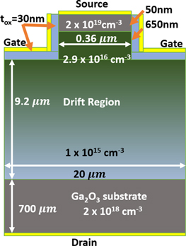
Figure 1. The structure used in this study. Dimensions and concentrations showed represent the best-calibrated values. The device is not drawn to scale for clarity.
Download figure:
Standard image High-resolution imageSince incomplete ionization and compensation doping are important in β-Ga2O3 devices,11,12 we propose PhuMob13 to be a more suitable model for electron mobility in β-Ga2O3. This is because it takes the screening of ionized impurities by charge carriers and temperature into account. This is particularly necessary when calibrating to cryogenic temperature experimental data. The PhuMob model is calibrated to the Si-doped Ga2O3 data in Ref. 14 at various temperatures and concentrations. The incomplete ionization model due to non-zero dopant ionization energy (ED) is turned on. Mobility degradation due to ionized dopant scattering is also enabled. This means that only ionized dopant will contribute to mobility degradation due to Coulomb scattering. The zero doping ionization energy of Si (ED0) is set to 52 meV with doping concentration (ND) dependent ionization energy coefficient, α, being 3.398 × 10⁻⁸ eVcm in the following equation from Ref. 10

The calibration results are shown in Table I. Figure 2 shows that the simulated temperature and doping dependent mobilities and free carrier concentrations agree well with the Hall measurement.
Table I. The PhuMob parameters calibrated in TCAD against the experiment. The symbols are the same as those in Table I of Ref. 13. The second column is calibrated against the Hall data in Ref. 14 and the third and fourth columns are calibrated against the device data in Ref. 4.
| As in Si10 | Si in Ga2O3 Bulk | Si in Ga2O3 Transistor NC = 0 | Si in Ga2O3 Transistor, NC = 7 × 1016cm−3 | |
|---|---|---|---|---|
| μmax (cm2V−1 s−1) | 1.417 × 10³ | 123 | 18.5 | 29.5 |
| μmin (cm2V−1 s−1) | 52.2 | 80 | 12 | 19.2 |
| θ | 2.285 | 1.8 | 1.8 | 1.8 |
| Nref,1 (cm−3) | 9.68 × 10¹⁶ | 2 × 10¹⁷ | 2 × 10¹⁷ | 2 × 10¹⁷ |
| α1 | 0.68 | 0.9 | 0.9 | 0.9 |
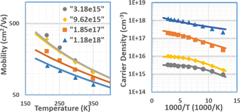
Figure 2. Comparison of calibrated TCAD PhuMob electron mobility (left) and Silicon ionization (right) simulation results vs experimental data in Ref. 14 of Silicon doped Ga2O3, for various Silicon concentrations.
Download figure:
Standard image High-resolution imageResults and Discussions
Effect of compensation doping
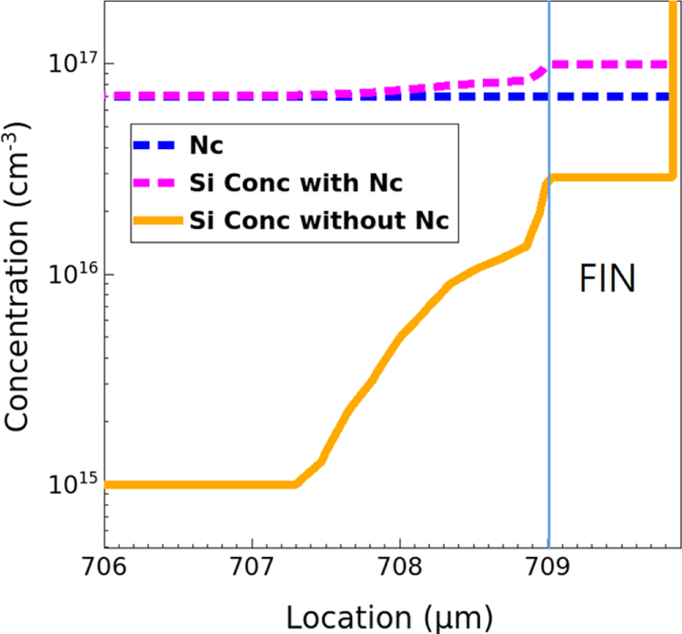
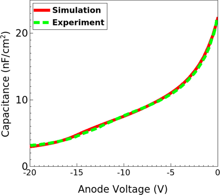
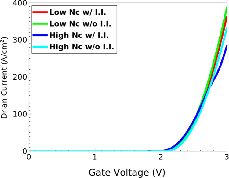
Compensation charges are inevitable in Ga2O3 due to its thermodynamic properties and growth method.11 Compensation charges are expected to be acceptors and usually have high ionization energies. It is expected to have a strong effect on the drift region's electrical properties, where n-type dopant concentration (ND) is maintained at a low level for high breakdown voltage. We study the compensation charge effect by considering two sets of drift region doping conditions. One is without compensation (NC = 0 cm−3) and one is with compensation (NC = 7 × 1016 cm−3) but both have the same ND-NC. The doping profiles studied are shown in Fig. 3. The net ND-NC distribution is derived by performing small-signal simulation to extract the capacitance of the MOS capacitor. Figure 4 shows that the results match the experimental CV result well. It is also found that capacitance depends only on ND-NC but very weakly on NC and its activation energy. On the other hand, NC has a strong effect on mobility as the ionized compensation dopants contribute to Coulomb scattering and thus degrades the ON current (ION) for the same ND-NC (Fig. 5). Moreover, incomplete ionization effect is more significant for higher NC. This is because high NC lowers the Fermi Level and exacerbates the incomplete ionization effect.

Figure 3. Activated Silicon and compensation doping concentrations (NC) of the simulation splits as a function of distance in the FIN and top drift region (vertical cut of Fig. 1).
Download figure:
Standard image High-resolution image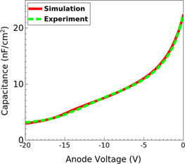
Figure 4. Experimental4 and simulated capacitance-voltage curves using the doping concentration in Fig. 3. With (not showed) and without (showed) compensation doping give similar results.
Download figure:
Standard image High-resolution image
Figure 5. Simulated ID-VG curves with and without incomplete ionization and with and without compensation doping. VD = 10 V. Note that they have the same ND-NC.
Download figure:
Standard image High-resolution imageInterface traps and sub-threshold slope
By applying the calibrated parameters in the second column in Table I, the doping profile in Fig. 3 with NC = 0 cm−3 and the given typical device dimensions (FIN width, wfin, = 0.33 μm and channel length, LG, = 0.8 μm) in Ref. 4, IDVG simulation is performed on the transistor in Fig. 1. Figure 6 shows the simulation results ("Default"). It can be seen that it overestimates ION and it has much steeper SS than the experiment. In order to match the experimental SS, interfacial acceptor traps are introduced at the gate insulator and Ga2O3 channel interface, which is a common practice to match the subthreshold slope and hysteresis in Si device when it has a significant density of interfacial traps. However, it is found that introducing traps at the interface does not change the SS. This is because the Ga2O3 device relies on bulk instead of surface (i.e. at the gate-insulator/semiconductor interface) conduction. For Silicon MOSFET, the conduction channel is formed at the gate oxide/silicon interface and thus, right before the ON state, the carrier concentration cannot be too low by definition. However, for this device, when it is in the subthreshold region, the surface can still have very low carrier concentration. The low carrier density is also a result of the much wider bandgap in Ga2O3. Therefore, the acceptors cannot be charged quickly enough to degrade the SS due to the lack of carriers.
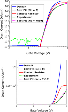
Figure 6. ID-VG curves from experimental4 and simulations with various setups. Top: Log scale; Bottom: Linear scale. "Default" is shifted −0.33 V for comparison. VD = 10 V.
Download figure:
Standard image High-resolution imageFigure 7 shows the change of conduction band edges (CBE) as a function of the gate voltage of the "Default" setting in the subthreshold region. One can see that right before ON state (VG = 2.17 V), the CBE at the center of the FIN is very close to the Fermi Level (i.e. ready to enter ON state). But at the insulation/channel interface, the CBE is still 1.1 eV above the Fermi Level and the electron density is only ∼0.1 cm−3. And at VG = 1.47 V, it is as low as 10−8 cm−3. The electron capture rate (c in s−1) to a trap can be expressed by10

where σ is the capture cross-section, vth is the thermal velocity and n is the electron density. For σ = 10−12cm2, vth = 107 cm s−1 and n = 0.1 cm−3, c = 10−6 s−1. This corresponds to a time constant of 106 s. Moreover, since the traps are expected to be deep, they also have long emission time. Therefore, the traps respond too slow to have an impact on the SS in regular measurement and in the TCAD simulation, one can consider the traps as negative fixed charges. In the following simulations, a fixed negative interface charge of ∼5 × 1012 cm−2 is therefore used and is similar to those deduced in Ref. 5. This is needed to match the threshold voltage, VTH, of the transistor.

Figure 7. The horizontal cut of the FIN in Fig. 1. Conduction band edge energies and electron quasifermi energies at various gate voltages of "Default" curves are showed. The gate voltages values refer to those in Fig. 6.
Download figure:
Standard image High-resolution image
Figure 8. Simulated breakdown curves at VG = 0 V with and without avalanche models and avalanche models with various parameters. "Scale" is the value multiplied to the pre-exponential factor in van Overstraeten—de Man model.
Download figure:
Standard image High-resolution imageIn summary, despite the fact that it is very possible that there is a high density of traps at the insulator/channel interface due to the immature technology in Ga2O3, it is believed that they do not contribute to the SS degradation. This may also be the reason for the low hysteresis observed in the experiment in Ref. 4.
Another possible reason for the worse SS in the experiment may be due to variation in gate insulator capacitance. The dielectric constant of the gate insulator (Al2O3) is thus intentionally modified significantly (5 instead of 9.1) for testing purposes but still cannot reproduce the SS in the experiment.
Finally, since short channel effect, such as Drain Induced Barrier Lowering (DIBL), is not negligible in the given dimensions,5 it is believed that the worsen SS is due to variations in the FIN dimensions (wfin and LG) in the device measured in Ref. 4. A careful inspection of the SEM in Ref. 4 shows that the average wfin is more than 0.33 μm and reaches ∼0.36 μm at the bottom of the FIN. LG is less 0.8 μm and is less than 0.7 μm after considering the 50 nm source region. The definition of LG is also ambiguous due to the asymmetric bottom corner rounding. Therefore, wfin and LG are varied to match the experimental SS. With wfin = 0.36 μm and LG = 0.65 μm, the SS can be matched well for both without compensation (NC = 0 cm−3) and with compensation (NC = 7 × 1016 cm−3) cases (Fig. 6, "Best Fit").
ION calibration
To match the ION, it can be assumed that there is a large contact resistance at the source and drain due to the immature technology. However, in order to match ION, an unreasonably high resistance (>18 mΩ cm2) is needed and only the current at VG = 3 V can be matched (Fig. 6, "Contact Resistor"). On the other hand, when the mobility parameters are further adjusted in PhuMob as shown in the third and fourth columns in Table I, it gives excellent matching to the experimental data in both subthreshold and ON regions. It can be seen that for the same ND-NC, larger NC results in larger mobility parameters (μmax and μmin) in PhuMob. Since only one of them is correct, for accurate modeling, it is important to perform physical characterization on the compensation doping concentration. Moreover, the PhuMob parameters calibrated to the transistor are much lower compared to those calibrated to the bulk Ga2O3 sample. It is possible certain scattering mechanisms are overlooked or the crystal quality in the experiment is not as ideal.
Breakdown mechanism
For breakdown simulations, van Overstraeten—de Man model is calibrated to theoretical calculation values in Ref. 16. The ionization coefficient is given by

where a and b are parameters and F is the electric field in V/cm.15 a is found to be 7.06 × 105 cm−1 and b is 2.1 × 10⁷ V cm−1.
To study the cause of the breakdown, VG is kept at 0 V and VD is ramped to high voltage. We only study the breakdown in Ga2O3 and assume the gate dielectric is intact. Since it has a premature breakdown due to gate rupture at ∼1000 V in the experiment in Ref. 4, the simulation result is not compared to the experimental result. Figure 9 shows the drain current as a function of VD. Simulation is performed with and without the avalanche model (impact ionization model). It is found that both have a breakdown voltage very close to 2200 V.

Figure 9. Distribution of impact ionization rate at 2170 V of the 2 device setups showed in Fig. 8. Left: Scale = 0.5. Right: Scale = 3.
Download figure:
Standard image High-resolution image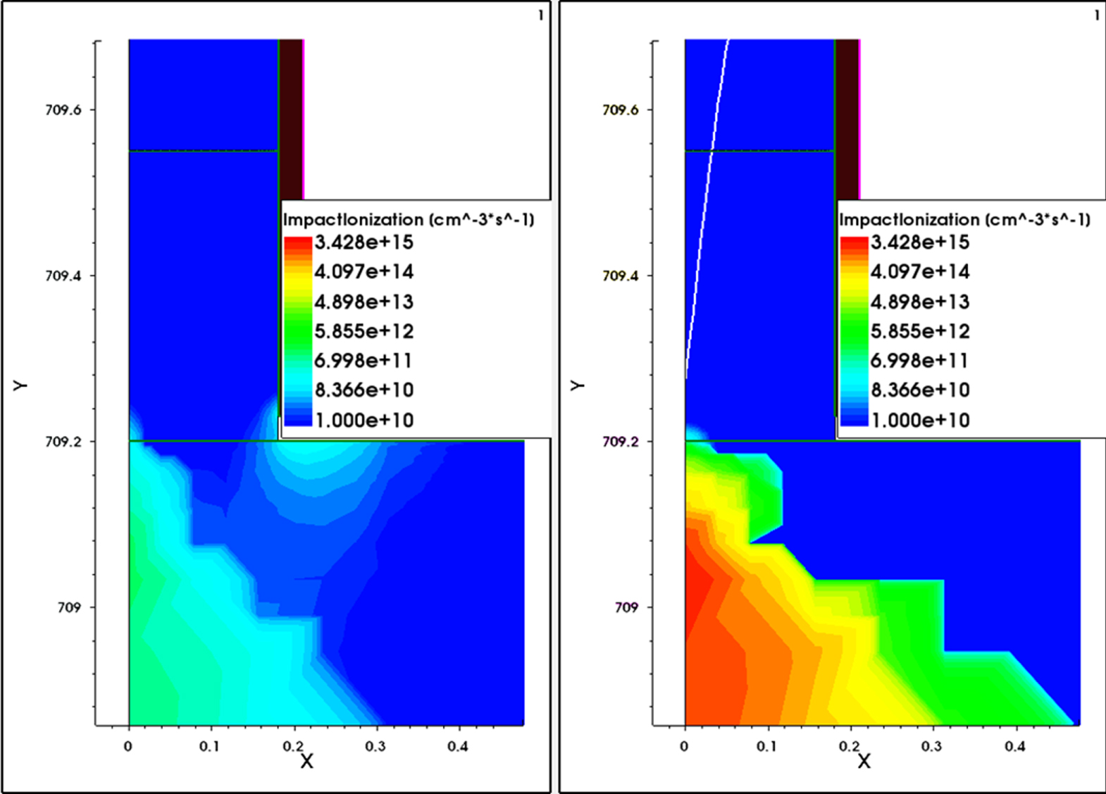
To further investigate the cause of the breakdown, the pre-exponent, a, of van Overstraeten—de Man model is deliberately increased by three times and decreased by half in two other simulations, resulting in six times of difference in a. It is found that the breakdown still occurs near 2200 V for both of them. If the breakdown is initiated by the impact ionization, it is expected that BV should be much higher when a is reduced by six times. Therefore, it is believed that the breakdown in the junctionless device is initiated by and the BV limited by punch-through.
Indeed, for the given b, if the potential drops evenly across the drift region, the electric field (2200 V/9.2 μm ∼ 2.4 × 10⁶ V cm−1 ∼ 0.1b) is still too slow to initiate avalanche breakdown at 2200 V. Therefore, the sharp breakdown when the avalanche is turned on in Fig. 9 is due to a punch-through initiated breakdown.
Figure 9 shows the avalanche rate of the devices at 2170 V and it can be seen that the highest avalanche rate is in the middle of the region right under the FIN. This is consistent with the explanation that the avalanche is triggered by the punch-through breakdown. A similar argument has also been reported for GaN junctionless device reported in Ref. 17.
Conclusions
A comprehensive calibration methodology for TCAD simulation of Ga2O3 devices is presented through the example of a multi-gate vertical device calibration. PhuMob is proposed to be a suitable mobility model in order to capture the temperature effect. It is shown that incomplete ionization and compensation doping have strong effects on device performance and should be included when necessary. It is also shown that insulator/channel interface traps do not contribute to the SS degradation of the junctionless bulk conduction devices. SS degradation is probably due to short channel effects. Finally, depends on the channel length, punch through can be the initiating factor of breakdown. Overall, the short channel effects (punch-through and VTH dependence of the width and channel length) of the junctionless device can be severe if the device is not designed properly.
Acknowledgments
The authors thank Synopsys Inc. for the donation of TCAD licenses. This work is supported by SJSU COE new faculty start-up fund.