Abstract
Integrated circuits currently use mainly copper as the interconnect material; unfortunately the ongoing miniaturization currently requires materials with higher electromigration resistance and possibly improved conductivity. In this context we report on the structure, microstructure and electrical properties of a series of Cu-Ge(O) alloy films, electrodeposited from an alkaline tartrate electrolyte. The composition of the films varies between zero and 20 at% Ge, with a significant incorporation of oxygen. Film morphology is dense and uniform, with Cu-Ge films exhibiting smaller apparent grain size (∼50 nm) with respect to Cu films grown from a similar electrolyte. Solid solutions and phase mixtures of a solid solution with the intermetallic are observed with increasing Ge fraction; the presence of intermetallic phases is confirmed by TEM imaging and diffraction. The resistivity of 50 nm thick films follows the published trend, with a slight increase of the value upon solid solution formation and a minimum in correspondence of the intermetallic composition. Thicker films (∼1 um) on the other hand show a different trend, with resistivity increasing with Ge and O at%; in this case the resistivity is probably dominated by the oxygen incorporation.
Export citation and abstract BibTeX RIS

This is an open access article distributed under the terms of the Creative Commons Attribution 4.0 License (CC BY, http://creativecommons.org/licenses/by/4.0/), which permits unrestricted reuse of the work in any medium, provided the original work is properly cited.
Since 1997, integrated circuits on semiconductor chips have been utilizing copper as the interconnect material.1 The interconnect structure usually consists of a suitably patterned, low dielectric constant (low-k) material deposited onto SiO2, followed by a diffusion barrier such as Ta or Ru, a Cu seed layer and finally electroplated copper, each film being sequentially deposited in trenches or vias, with the smallest width decreasing steadily with each technology node, currently being between 14 and 22 nm. This miniaturization trend resulted in evaporated Aluminum being displaced by Copper, a more conductive material with higher electromigration resistance that became necessary to minimize the RC delay while also improving the mechanical and electrical properties.2,3 This design has served well until recent years; with further decrease of the minimum features of interconnect lines however the Cu resistivity increases due to spatial confinement, and electromigration becomes once again an issue due to higher current densities. It has therefore become necessary to minimize the footprint or altogether eliminate some of these layers4 by (i) introducing interconnect materials, typically Cu with a strong oxide former,5 that would spontaneously form a diffusion barrier upon annealing, or (ii) add alloying elements to Cu in order to enhance mechanical and diffusion barrier properties.6,7 A detailed selection of suitable alloying elements to Cu has been carried out by Barmak et al.8 on the basis of resistivity vs. at% of solute and the configuration of the phase diagram. Ten elements were identified in this work for future investigations of their behavior against electromigration and/or voiding.
Several efforts did target dilute Cu alloys to decrease transport at grain boundary,9 while others focused on Cu silicides, which unfortunately exhibited high resistivity, of the order of 100 μOhm-cm.10 In sharp contrast, Cu germanides achieve a combination of low resistivity and strength suitable for these applications. The intermetallic Cu3Ge in particular was first synthesized by IBM using E-beam evaporation, showing a resistivity around 5.5 μOhm-cm (at 10–200 nm thickness)9,11 and excellent oxidation resistance up to 450°C.12 Cu3Ge has later been grown by distinct deposition methods and on various substrates; in particular, it was epitaxially grown onto c-sapphire by PLD, showing a resistivity of 6 ± 1 μOhm-cm;13 this work was followed up with a new series of measurements at the nanoscale, confirming the previous data.14 CVD of Ge at 250°C onto Cu films and in trenches resulted in formation of Cu3Ge, which was stable up to 600°C; no data on resistivity however were given.15 E-beam evaporation was also used to deposit Cu3Ge on Si(100) by first depositing Ge followed by a Cu layer. Si diffused through the interface but the resistivity remained low, 10 to 15 μOhm-cm up to 600°C.16 Very low contact resistivity of Cu3Ge with n-GaAs (7 × 10⁻⁷ Ohm-cm2) was demonstrated,17 suggesting compatibility with a variety of substrates.
Since the current manufacturing process for Cu interconnects is electrodeposition, the ability to electrochemically grow Cu3Ge would open the opportunity to directly integrate this or any other alloy within the manufacturing flow. Cu3Ge has indeed been grown by electrodeposition using an alkaline tartrate solution and pulse plating; the resistivity measured after annealing was high, 45 μOhm-cm, attributed to the small grain size and impurities, mostly oxygen.18 In our own work19 we have investigated the mechanism of the codeposition process, of importance in the context of fundamental electrodeposition, since pure Ge grows in aqueous solution only up to a few atomic layers, due to the strong hydrogen evolution occurring after few monolayers of Ge are deposited. We found indeed a novel mechanism whereby Ge can continue to grow in parallel with Cu reduction, owed to Ge interactions with Cu at the interface.
In this work we describe the main features of the electrodeposition process of Cu-Ge alloys, discuss the film morphology and structure, and report the electron transport properties of these alloys. We find that low resistivity films, close to those obtained by vacuum deposition, can be obtained by electrodeposition at low film thickness; on the other hand thicker films present higher resistivities, induced by the incorporation and precipitation of significant oxide phases.
Experimental
Electrochemistry
Cu and Cu-Ge films were grown at room temperature in a three-electrode electrochemical cell; a Ru(100 nm)/Ta(10 nm)/Si wafer was used as the cathode; the counter electrode was a platinized Ti mesh and the reference electrode was a saturated Ag/AgCl (EAg/AgCl = 197 mV vs SHE); in the following, potentials will be referred to this scale. An alkaline electrolyte developed by Joi et al.18 was used to grow the Cu-Ge films; the electrolyte contained 25 mM CuSO4, 100 mM GeO2, 300 mM C4H4K2O6 (potassium tartrate) and 325 mM NaOH; pH was adjusted to 13. Linear Sweep Voltammetry (LSV) was carried out between −0.95 and −1.85 V, with a scan rate in the negative direction of 10 mV/s. A Bio-logic SP300 potentiostat was used to control and monitor the electrodeposition process.
Materials characterization
Film morphology was investigated with a FEI Quanta 650 Scanning Electron Microscope (SEM). Images and Energy Dispersive Spectrometry (EDS) line scans of cross sections were obtained with a JEOL JSM6701F SEM. The chemical composition of the films was determined by the EDS system attached to the Quanta 650 SEM. EDS data were collected with an accelerating voltage of 20 kV; 5 spots per sample were used to determine the nominal composition and the standard deviation was no higher than 1.5%. The crystallographic structure of the films was established by X-ray diffraction (XRD), using a PANalytical X'Pert Pro MPD instrument with Cu Kα radiation (λ = 1.5406 Å) in a symmetric θ-2θ configuration. Electrochemical anodic dissolution of as grown films with various composition was also carried out at 5 mV/s in the electrolyte used for electrodeposition in order to provide further insight on the phase constitution.
X-ray Photoelectron Spectrometry (XPS) experiments were performed using a SPECS PHOIBOS 100/150 spectrometer with monochromatic Al Kα X-rays with a pass energy of 50 eV. The resistivity ρ was obtained using the van der Pauw method20 with the 4 point probes close to the edges of the samples and using Equation ρ = 4.532·t·R12,34, where t is the thickness of Cu-Ge films and R12,34 is the resistance calculated from the ratio between the voltage at contacts 3 and 4 and applied current at contacts 1 and 2.
Results and Discussion
Electrodeposition
Fig. 1 shows the linear sweep voltammetry (LSV) behavior for the Cu-Ge electrolyte and the film composition as a function of applied potential. Based on our previous work,19 in the potential window −1.0 to −1.2 V Cu is deposited while GeO2−3 is reduced to GeOH and adsorbs at the substrate; at more negative potentials Ge species are reduced to GeH, causing significant hydrogen evolution and starting to interact with Cu at the interface (−1.2 to −1.4 V). At an even more negative potential the Cu fraction is further decreased when the rate of Ge codeposition significantly increases due to the full activation of the Ge-H bond via a strong interaction with Cu, leading in parallel to an increase in oxygen incorporation. Cu deposition from a similar electrolyte (without Ge salts) exhibits a higher efficiency at low overpotential (Fig. 2), due to the passivation of the surface by adsorption of GeOH. Also, at high overvoltage the Cu-Ge presents a lower efficiency, due probably to the strong hydrogen evolution induced by the interaction of Ge-H with Cu. The relatively high content of oxygen in the films grown at high overvoltage (Fig. 1) is probably owed to the pronounced adsorption and incorporation of GeOH, GeOOH species within the growing film.

Figure 1. (a) Linear sweep voltammetry for the Cu-Ge electrolyte; (b) Alloy composition vs. applied potential.
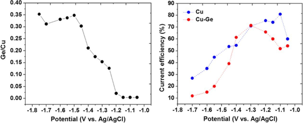
Figure 2. (a) Ge/Cu atomic ratio vs. applied potential. (b) faradaic efficiency for Cu and Cu-Ge electrodeposition from a tartrate based alkaline electrolyte, pH 13.
Electrodeposition experiments under potentiostatic conditions show that the Ge fraction increases monotonically with overpotential, achieving a saturation value of about 20 at% (30–35 at% Ge/Cu). Oxygen fraction follows a similar trend, with O starting to be incorporated below −1.2 V, showing a shallow maximum followed by an approach to saturation (Fig. 1b). Note that the O fraction follows closely the Ge fraction, suggesting that a significant fraction of Ge may be bound to Oxygen.
Film morphology
Figs. 3a, 3b shows the morphology of pure Cu electrodeposited from the alkaline solution (without Ge ions) at two distinct applied potentials, −1.05 and −1.5 V. The deposit at −1.05 V consist of compact, uniform pyramidal-shaped grains with an apparent grain size of <100 nm. The deposit obtained at −1.5 V in contrast shows larger and faceted grains with a more pronounced topography, showing in several locations pentagonal symmetry, suggesting the presence of multiple twinning or disclinations.21 Both films incorporate small amounts of oxygen, 2.4 and 1.7 at%, respectively. It should be noted that the formation of larger apparent grains at higher overvoltage is against the prediction of nucleation theory, suggesting the occurrence of a different growth mechanism. We speculate that the increased surface pH induced by the strong gas evolution at more negative voltage may generate more Cu oxide/hydroxide adsorbed species that could block a fraction of the active sites, leading to grain outgrowth from the remaining active sites.
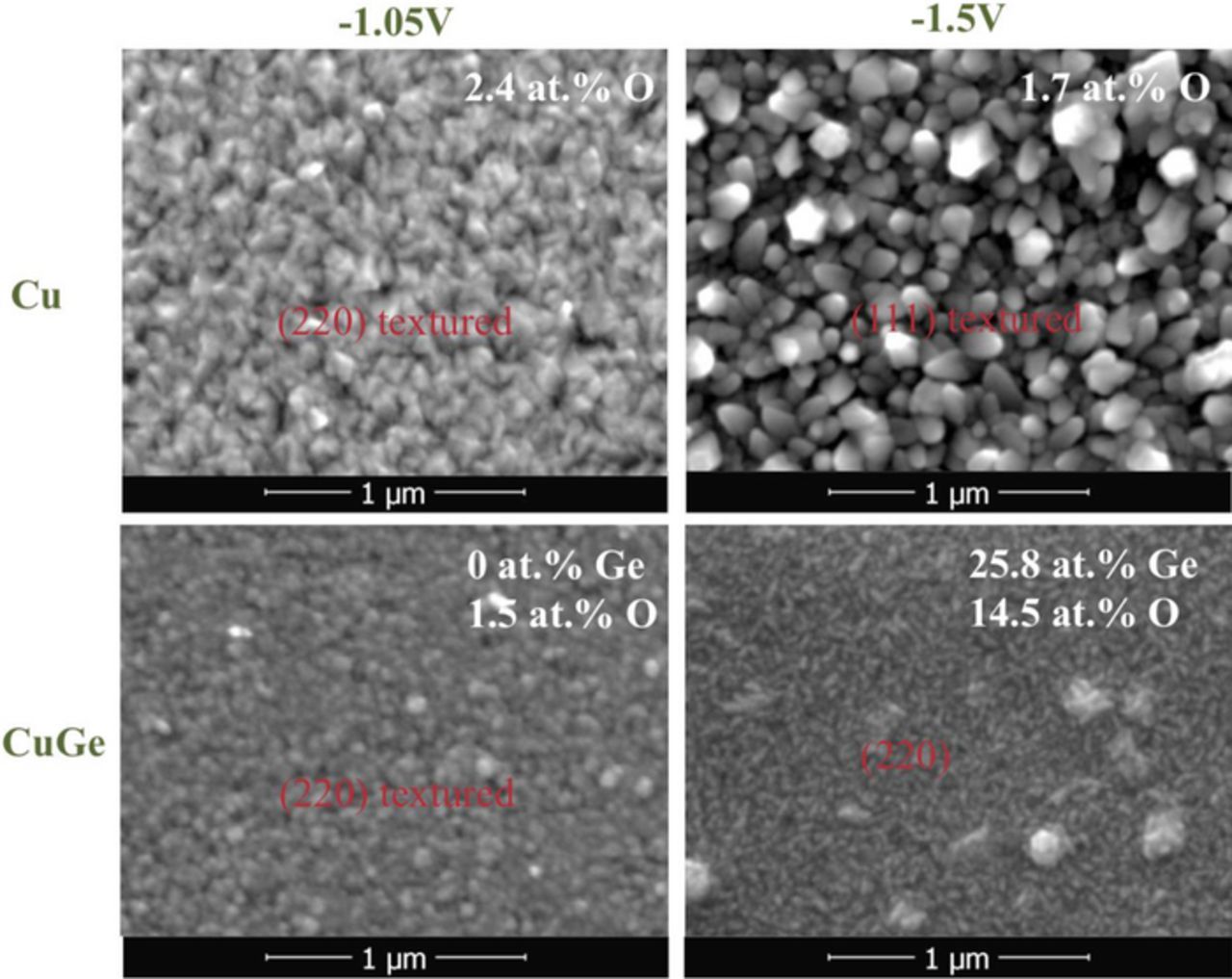
Figure 3. Morphology of selected Cu and Cu-Ge films grown at −1.05 and 1.5 V; shown are also the oxygen content and the alloy composition.
With addition of Ge salts in the electrolyte, the grain size decreases significantly even if no Ge is being incorporated (Fig. 3c), consistent with a growth mechanism whereby GeOH species adsorb and inhibit growth. Films grown at large overvoltage (Fig. 3d) exhibit elongated grains and some clustering, probably formed under conditions of strong hydrogen evolution in parallel with oxide precipitation and incorporation of large amounts of Ge.
A magnified image of a ∼25 at% Ge film (Fig. 4a) shows that the apparent grains are made up of smaller grains that are not properly resolved but show an apparent size of less than 50 nm. A cross section is also shown of an 18 at% Ge film (Fig. 4b), showing a relatively smooth surface and columnar grains oriented at about 55 degrees from the surface plane, suggesting a biaxial texture.

Figure 4. (a) Magnified view of the surface morphology of a 25 at% Ge Cu-Ge film; (b) Cross section of an 18 at% Ge, Cu-Ge film.
Structural investigations
Pure Cu grown from this alkaline tartrate electrolyte presents a FCC structure, with a (220) preferential orientation at low overvoltage and a (111) orientation at high overvoltage (Fig. 5).
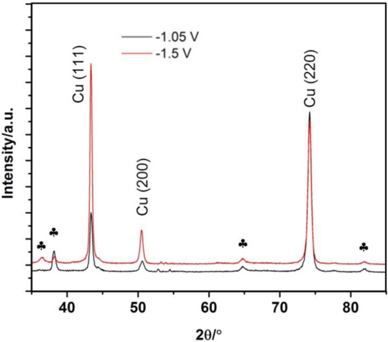
Figure 5. XRD patterns of Cu films grown from an alkaline tartrate electrolyte.
The Cu-Ge binary system22 evidences a solubility for the FCC phase up to ∼10.8 at%, followed by a narrow stability range for the HCP phase; three intermetallic compounds with a limited homogeneity range ɛ (Cu3Ge, monoclinic), θ, η, are present, the first two stable only at high temperature, and the latter stable down to room temperature. Fig. 6 shows a set of XRD patterns for Cu-Ge films with different compositions, compared to a Cu film grown at low overvoltage from the same electrolyte. With increasing applied overvoltage for Cu-Ge films, we observe a decrease in the intensity of the (220) peak, an increase in the (111) peak, and a shift for both of these peaks to lower angles, corresponding to an increase in lattice constant, due to the larger atomic radius of Ge (211 pm for Ge vs. 128 pm for Cu). Traces of the intermetallic phase are seen already in the 11 and 19 at% Ge films, suggesting a biphasic microstructure. In the close-to-stoichiometric Cu3Ge (25.8 at% Ge) it is found a small amount of Cu(220) and two peaks corresponding to the ɛ phase. By further increasing the Ge fraction, the intensity of these intermetallic peaks increases; no XRD evidence of Ge precipitation is visible, probably because of its dispersed nature. It should be noted that the formation of an intermetallic phase is quite unusual when film growth is carried out by room temperature electrodeposition; some examples are the formation of chalcogenides or binary alloys including at least one low melting point metal; Cu and Ge do not satisfy this connotation, suggesting that the energy barrier for the formation of such monoclinic structure could be small and/or adatom diffusion along selected directions may be unusually fast.
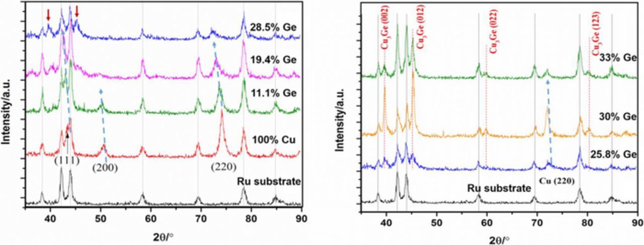
Figure 6. X-Ray Diffraction patterns for electrodeposited Cu-Ge films with various compositions, compared to a Cu film grown at low overvoltage. Phase transitions FCC ⇒ ɛ are seen with increasing Ge fraction.
In order to better understand the phases present in the Cu-Ge films and supplement the XRD data, we used also an electrochemical dissolution procedure (anodic stripping) on selected Cu-Ge films grown at −1.05 V (98 at% Cu), −1.3 V (83 at% Cu), and −1.5 V (67 at% Cu) (Fig. 7). Two main dissolution peaks are evidenced in the 98 at% Cu film (Cu), suggesting the formation of two distinct Cu microstructures; the Cu 83% film shows an additional dissolution wave that can be assigned to the dissolution of Cu bound to Ge; the 67 at% Cu film in contrast presents three additional shoulders or peaks, that are assigned, from the more negative (less noble), to Ge and two more forms of Cu-Ge that could be assigned to the intermetallic phase. Next we turn to TEM and XPS characterization that may help to achieve further insight in these additional phases.
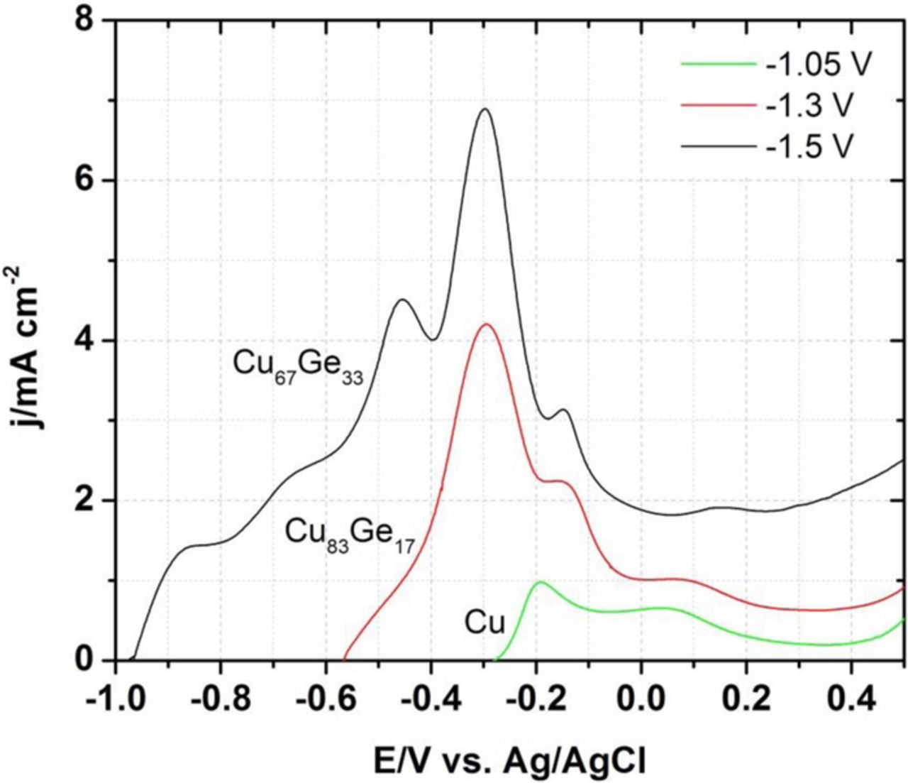
Figure 7. Anodic stripping data (5 mV/s) for pure Cu and two Cu-Ge films with distinct composition; the data show the presence of distinct phases in the films.
TEM
A Ge 26 at% Cu-Ge film with a high volume fraction of the intermetallic phase was investigated in detail (Fig. 8). A cross sectional view of the film is shown on the left, where the Cu-Ge film shows a clear contrast against the Ru substrate; the film surface does appear uneven. Two locations in the film, the bottom and the top of the Cu-Ge film, as highlighted at the left, are selected for high resolution imaging. The bottom region displays the main presence of ɛ-Cu-Ge and hexagonal ζ-Cu-Ge (the latter not seen by XRD, suggesting a low volume), plus some amorphous Cu as highlighted by a halo diffraction ring. The Fast Fourier Transform (FFT) of the bottom region shows the presence of few reflections related mostly to ɛ-CuGe. The ζ phase is adjacent to grains of the ɛ-phase; it has been demonstrated that the disordered hexagonal ζ phase can epitaxially relate to the ɛ-phase by a minor arrangement on the [0 0 0 1]hcp plane.23 Finally, the top region also shows the presence of ɛ-phase and amorphous Cu; based on the FFT pattern, amorphous Cu and/or Cu-Ge may comprise a larger fraction of the film volume.
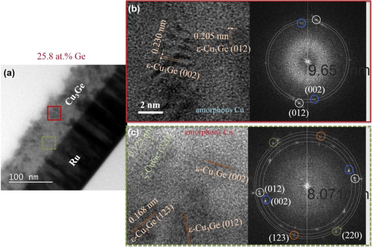
Figure 8. (a) Cross sectional TEM image of a Cu3Ge film; (b) high resolution TEM and FFT analysis of a region close to the surface, and (c) high resolution TEM and FFT analysis of a region close to the substrate.
XPS and EDS line scans
Figures 9a and 9b depict the XPS spectra of Cu-L edge for samples containing 2 and 18 at% of Ge, respectively. The peaks for L3 and L2 edges indicate the presence of metallic copper and Cu+ oxidation state on the surface. The peak deconvolution displayed in this figure confirms that the majority of copper atoms are in a metallic state, and just a small portion (probably in the outermost surface layer) is in the Cu2O state. The low intensity of the satellite peaks at about 942.5 and 946.5 eV also confirms the metallic state of Cu in both samples.

Figure 9. XPS spectra for Cu-L edge of samples with (a) 2 and (b) 18 at% of Ge, and for Ge-M edge of samples with (c) 2 and (d) 18 at% of Ge.
Figure 9c shows the Ge-M edge for a sample containing 2 at% of Ge, where two main peaks are evident at about 29.7 and 31.8 eV, labeled as metallic Ge and Ge oxides, respectively. The metallic peak has a low intensity and the oxide peak can be deconvoluted in two contributions, one at 31.5 eV due to GeO and the other one at 32.5 eV due to GeO2, indicating that both oxides are present in the sample. Figure 9d displays the Ge peaks for sample with 18 at% of Ge. In this case, only oxide peaks are observed, with an increase of the GeO contribution in relation to GeO2.
Figures 10a and 10b presents the composition profiles of samples with 2 and 18 at% of Ge, respectively. The profiles were obtained by line scanning EDS measurements along the cross section of the deposits. The graphs indicate that the films start to grow with a higher concentration of Ge and O relative to Cu that eventually evolves to a uniform composition along the layer. The graphs also show that O follows the profile of Ge, and also a higher concentration of Ge results in higher amounts of O. The composition profiles in Figure 10 are qualitatively in agreement with the data in Fig. 1, also showing an increase in O fraction when the Ge fraction increases.
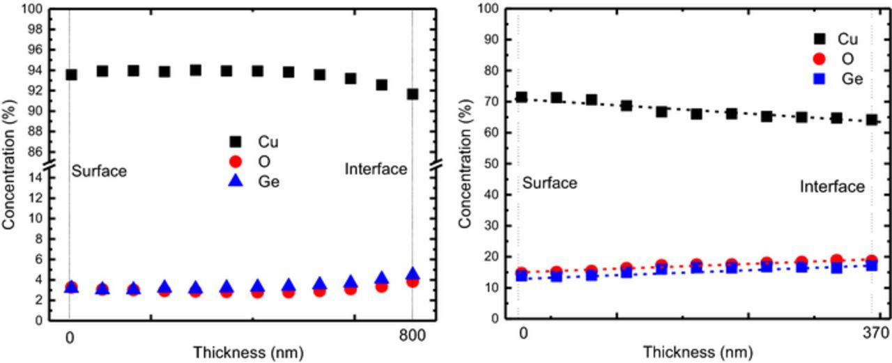
Figure 10. EDS Composition profiles of a samples with (a) 2% of Ge and thickness of 790 nm and (b) 18% of Ge and thickness of 370 nm.
Film resistivity
The resistivity of 50 nm thick Cu-Ge films as a function of composition reflects roughly the various alloy phases that are present in the films (Fig. 11). With increasing Ge, and in the range of solubility of Ge in FCC Cu, the resistivity increases from 7 μOhm-cm, that should be compared with 1.7 μOhm-cm for bulk Cu, to 12 μOhm-cm at 14 at% Ge. Beyond 14 at% Ge the resistivity decreases, probably due to the presence of mixed phases, the (super)saturated solid solution and the ordered phase ɛ-Cu3Ge; no evidence of the hexagonal phase is present. At about 25 at% Ge the resistivity reaches a minimum of about 8 μOhm-cm, after which the resistivity increases again. This behavior is qualitatively consistent with published results, showing that there is a minimum in the resistivity vs. composition associated with the ɛ-Cu3Ge intermetallic composition. It should be noted that the resistivity values reported herein are higher than the best results reported by others; the resistivity of Cu in this work is about 3 times higher than bulk Cu, and the intermetallic phase shows a resistivity 40% higher than the best values reported by the IBM group. These discrepancies can be probably explained based on the incorporation of oxides, generated at the growing interface and eventually being incorporated.
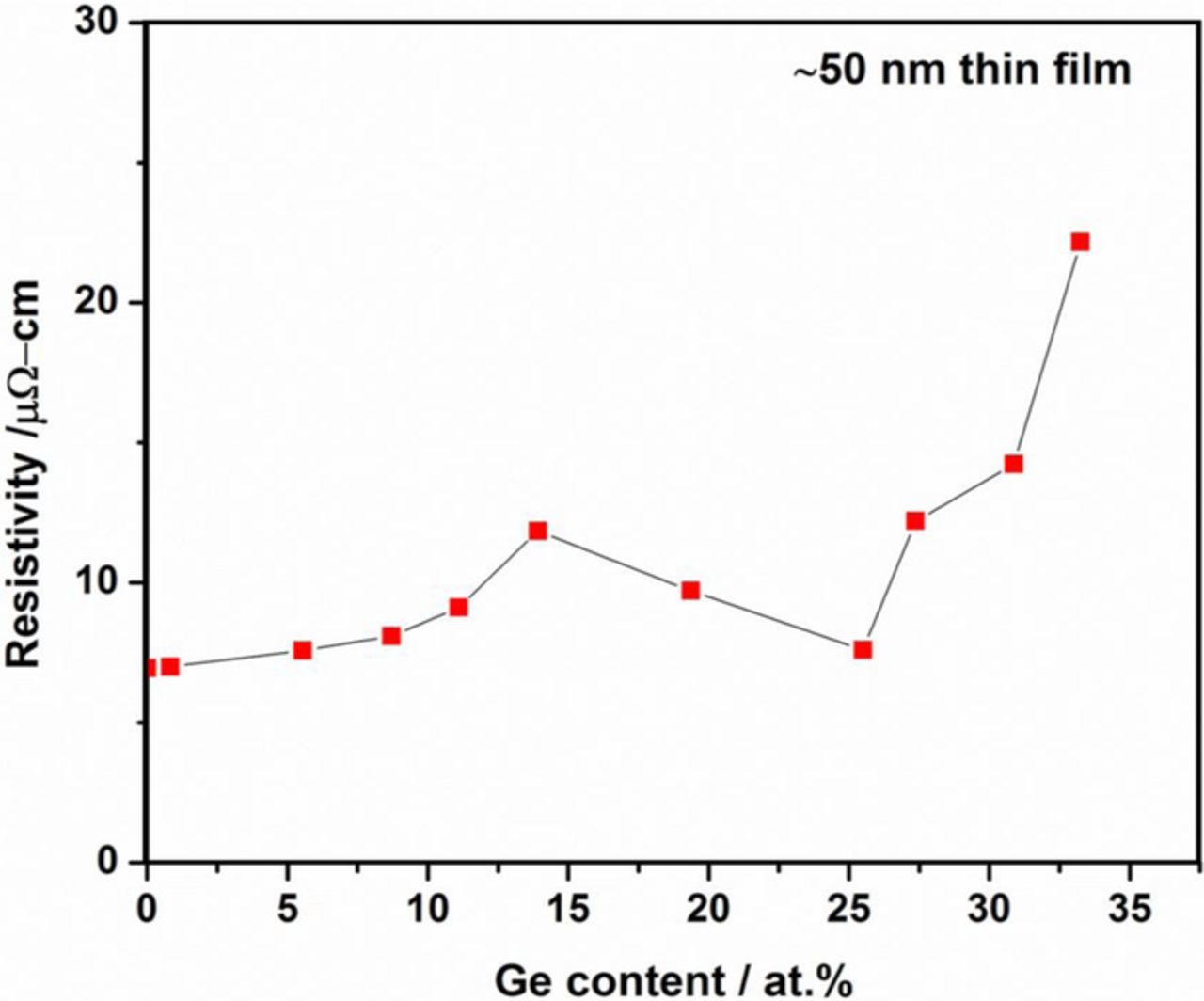
Figure 11. Van der Pauw resistivity measurements at room temperature as a function of film composition; film thickness is 50 nm.
An additional series of resistivity measurements were carried out on ∼1 μm thick films; these samples showed in general a higher resistivity, with a clear but scattered trend toward higher resistivity for higher concentration of Ge and O, as shown in detail in Figure 12. No apparent minimum in the vicinity of 25 at% Ge was observed in these films, suggesting that the resistivity is now dominated by the amount and the distribution of oxygen throughout the film. The observed increase in the oxygen fraction in thicker films could be due to the longer duration of the electrodeposition process, whereby the electrolyte may become partially unable to buffer, thus resulting in a higher electrolyte pH, as confirmed by post-deposition pH measurements. Most of the resistivity values are between 10 and 30 μOhm-cm, with lower resistivities being obtained for lower Ge and O fractions, suggesting that it may be possible to decrease these values by targeting a lower oxygen content, for example by pulsing the waveform during electrodeposition,18 or by combining annealing in a suitable atmosphere.
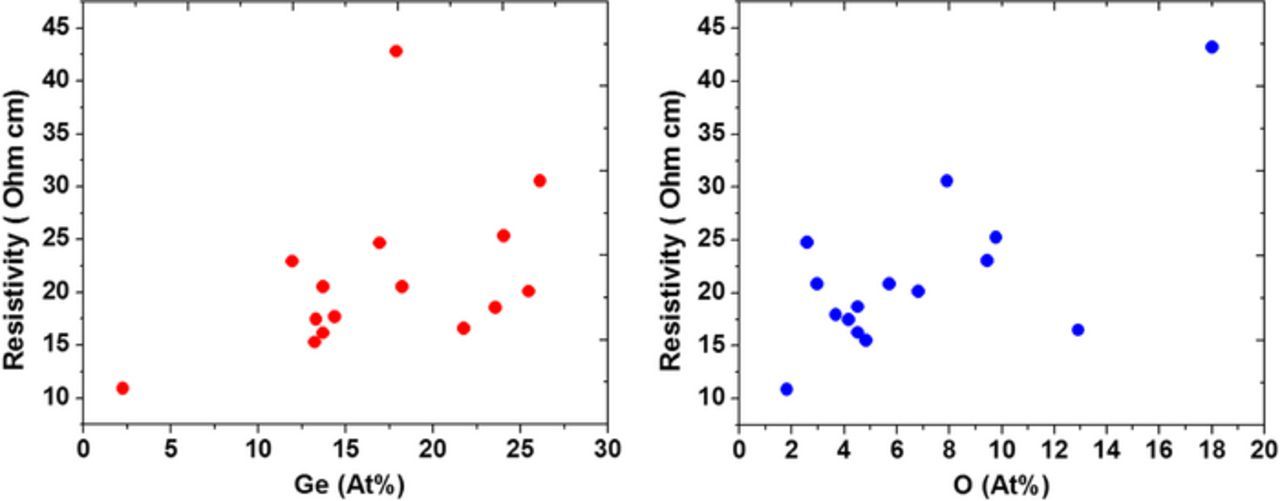
Figure 12. Resistivity of Cu-Ge films as a function of Ge at% and O at%.
Finally, Figure 13 shows the resistivity ρ as a function of temperature between 20 and 300 K for samples with 2 and 18 at% of Ge and room temperature resistivities of about 11 and 43 μΩ-cm, respectively. For the sample with lowest Ge concentration the curve displays a straight linear behavior at temperatures higher than 100 K, as expected for metallic systems where the law ρ ∼ T is observed. The resistivity vs. temperature for the sample with highest amount of Ge in contrast tends to show a constant value for low temperatures (below 50 K) and to saturation for high temperatures (above 250 K). The resistivity goes to a limiting value following a ρ ∼ T0.2 law, a trend that is observed in systems where the carrier mean free path is comparable to the lattice parameter.24 The low mean free path is probably due to the high amount of O of 18 at% diluted in the Cu-Ge lattice.

Figure 13. Electrical resistivity vs. temperature for the samples with 2% (red) and 18% (black) of Ge in Cu-Ge samples.
Conclusions
Cu-Ge(O) films with a wide range of composition have been grown by electrodeposition. The films present small grain size and a dense morphology. The crystal structure of these films depends on composition; up to about 11 at% Ge the films are FCC solid solutions, while at higher Ge at% the films exhibit a mixture of a solid solution and a monoclinic structure. TEM images of ∼25 at% Ge films confirm the formation of the intermetallic structure ɛ-Cu3Ge. The resistivity of 50 nm films follows the trend of previous reports, showing a minimum of resistivity of 8 μOhm-cm around 25 at% Ge, while thicker films show a resistivity that seems mainly dependent on the incorporation of oxygen and germanium. Cu-Ge alloys can be probably formed only at low thickness, while further growth, around 1 μm thickness, results in an increasing precipitation of oxides, leading to Cu-Ge(O) films.
Acknowledgments
The investigators from Brazil thank the financial support from CAPES and CNPQ. The authors also thank Alexandre Mello and the Laboratório de Superfícies e Nanoestruturas-LabSurf (CBPF) for the XPS measurements.