Abstract
In the pursuit of a photosynthetic and efficient water splitting device, detailed investigations of individual aspects of the whole device are necessary: catalysis, electronic conductivity, cathode and anode stability, and kinetics among other aspects. Improvement in one aspect can, however, often require fundamental tradeoffs affecting others. High solar-to-hydrogen efficiency of the overall system is the ultimate goal of water splitting research. When optimizing half-cells, either the anode or cathode, the photovoltage required to achieve a current density of interest is an especially important metric. This report investigates the photovoltage in insulator-protected water oxidation anodes using ALD-TiO2 protected silicon devices as a case study and looks in depth at how photovoltage is correctly determined from typical electrochemical analysis and how this relates to the underlying solid-state carrier transport. Finally, the photovoltage at 10 mA/cm2 referenced to the thermodynamic potentials is reviewed from several leading research reports for various photoanodes and photocathodes, providing a direct comparison of cell performance.
Export citation and abstract BibTeX RIS

This is an open access article distributed under the terms of the Creative Commons Attribution 4.0 License (CC BY, http://creativecommons.org/licenses/by/4.0/), which permits unrestricted reuse of the work in any medium, provided the original work is properly cited.
Half-cell efficiency and photovoltage metrics
The solar-to-hydrogen (STH) efficiency is the most important metric for characterizing water splitting cells, and can be calculated in a variety of ways. When optimizing an anodic or cathodic half-cell, the implied-efficiencies are often reported as the product of the photovoltage and current, divided by the input solar power. The power point of an actual water splitting device, however, will be determined by current matching among the components, and also necessitates a minimum voltage to drive the reactions of interest. As such, implied half-cell efficiency plots as a function of voltage can include values that are not meaningful for full cell operation. As will be shown at the end of this report, most reported anodes and cathodes do not yet provide sufficient photovoltage for photosynthetic operation of full water-splitting cells, meaning the current stand-alone full cell efficiency is still zero.
The closest metric to efficiency that can be easily compared from report to report and used to best imply final device operation is the photovoltage at a relevant current, namely the voltage given to or required from the rest of the device, including the other half cell, at a certain operating current. When the photovoltage is measured close to zero current, an approximation of the open-circuit photovoltage is obtained. When it is measured at a reasonable operating current like 10 mA/cm2, an approximation of the power given or needed at the max power point is obtained. The tables at the end of this report show the voltage provided from a given half-cell and needed from the other at 10 mA/cm2 to illustrate these comparisons.
Comparing experimental results to theory helps illustrate the difference between half-cell and full-device efficiency calculations and how to transform values between the two. Pinaud et al. have attempted to calculate the practical, theoretical limit of solar-to-hydrogen efficiency factoring in 1) Butler-Volmer kinetic losses of the best catalysts available and 2) energy and entropic losses from defects and non-radiative recombination for reasonable open-circuit photovoltages.1 The maximum efficiency for a cell with a single photoelectrode is found to be 11.2% with a bandgap of 2.26 eV, or 22.8% for a tandem device with two photoelectrodes with bandgap 1.23 and 1.84 eV.1 As very few full devices have been experimentally fabricated so far, most work focuses on cathodes or anodes. For photocathodes, a long-time half-cell efficiency record of 16.2% or 13.3% was established by Heller in 1982 with InP nanopillars and a Pt catalyst for the HER half reaction.2 The higher 16.2% value is calculated from the conserved energy as referenced to a smooth Pt electrode reference and the lower 13.3% value to a fuel cell operating at the thermodynamic potential with no kinetic losses. These efficiencies represent the photovoltage-photocurrent product achieved for solar illumination with respect to a certain chosen reference. The full-cell efficiency is the result of the power generated by the current-matched half cells. Given the specific reference chosen, half-cell efficiencies, such as those given above from Heller's work, will typically be higher than the final full-cell efficiency, which can only be determined once both half cells are defined. For this reason, these half-cell efficiency values can fall above the practical full-cell theoretical maximum as calculated by Pinaud et al. of 11.2%.1 Another common reference for half-cell efficiency is illustrated by Lee et al. who used a nanopillar structure to achieve a 14% half-cell efficiency calculating this as the photovoltage referenced to the theoretical potential of the H+/H2 reaction multiplied by the current and divided by the input solar power.3
These two prior reports illustrate the indirect nature of half-cell efficiency calculations in pointing toward the ultimate solar-to-hydrogen efficiency possible. As recommended in a recent review of the field,4 the photovoltage at a reasonable operating current such as 10 mA/cm2 likely represents the best alternative performance metric to half-cell efficiency because it more directly states the ultimate utility of the device. Elsewhere in this paper, various literature results will be compared using this photovoltage metric. For any electrocatalytic device operating typically as a half-cell in a three electrode configuration, figures of merit include the Tafel slope, exchange current density, turnover frequency, and overpotential at specific current densities. For any solar cell, figures of merit include, the open-circuit photovoltage, fill factor, and short circuit current density. For a photoelectrochemical half-cell, the photovoltage at meaningful current densities serves as the single most important metric when pointing toward its utility for the end application.
Analytical understanding of photovoltage in insulator-protected cells
In this paper, analytical models are presented for measuring and quantifying photovoltage from water-oxidation anodes, as well as from reversible redox electrodes (specifically using the ferri/ferrocyanide redox pair). Successful insulator protection of silicon photoanodes used for water oxidation was described in 2011 in work from our laboratories. Ultrathin (1-2 nm) TiO2 layers deposited by atomic-layer deposition (ALD-TiO2) protected nSi photoanodes for over 8 hours without signs of decay.5 In 2013, we showed that relatively efficient hole conduction was possible through thicker TiO2 up to 12 nm in thickness with only modest increased applied voltage required in p+Si anodes measured in the dark.6 These ALD-TiO2 protection layers were shown to have a resistivity of about 2 × 10⁸ Ω·cm, thus acting like leaky insulators. Our most recent work has found that ALD-TiO2-protected nSi exhibits a significant photovoltage loss with increasing TiO2 thickness, suggesting increased recombination of the photo-generated holes as the TiO2 thickness is increased, a loss mechanism that is not observed for TiO2-protected p+Si anodes in the dark. In support of this explanation, it was found that TiO2-protected p+nSi buried junctions, designed to maintain a high hole density at the oxide/silicon interface, provide large photovoltages that are nearly independent of TiO2 thickness, including a record 630 mV photovoltage despite the presence of a 8 nm thick protective TiO2.7 In 2014, work by researchers at the Joint Center for Artificial Photosynthesis (JCAP)8 produced ALD-TiO2 protection layers with similar methods to previous work,5-6 but with much lower resistivity. However, these more conductive TiO2 layers deposited on nSi anodes exhibit significantly lower photovoltage than seen with thin insulating ALD-TiO2 on nSi5,7,8 presumably due to the replacement of a metal-insulator-semiconductor (MIS) junction by a semiconductor-insulator-semiconductor (SIS) junction between the heavily doped TiO2 and nSi. As shown in this paper, the disparity between photovoltage provided by even the best half cells and that needed for a stand-alone full cell water splitting device means that increasing photovoltage is of paramount importance. To that end, providing an understanding of photovoltage in metal-oxide-protected devices, how it is correctly determined and how it relates to ultimate device performance, is the main goal of this work.
Here, as a case study, we investigate sources of photovoltage loss for forward and reverse currents in ALD-TiO2 protected water oxidation structures: p+Si/SiO2/TiO2/M, nSi/SiO2/TiO2/M, and p+nSi/SiO2/TiO2/M where M is any high work function metal (e.g. Ir, Pt, or Ni). This analysis provides a model of the photovoltage measured for water oxidation, or for a reversible redox couple such as ferri/ferrocyanide, as is common practice in the field. A simple relationship is derived between photovoltage measured for water oxidation and for a reversible redox couple. In the last section of the paper, we compare the implied performance of leading research reports of water-oxidation photoanodes and water reduction photocathodes presented as tables of photovoltage at a constant current density.
Results
The p+Si reference anode
A common practice when studying water splitting half-reactions is to use a degenerately doped reference semiconductor working electrode that is capable of providing the same chemical and solid-state matrix as a photoelectrode, but in which a high surface carrier concentration is achieved by doping rather than light absorption. Among the most important attributes of the reference working electrode, compared to the corresponding photoabsorber substrate for insulator-protected cells are 1 – similar surface chemical bonding of the overlying insulator and/or of catalyst layers and 2 – similar electrochemical potential of the hole (for water oxidation) or electron (for water reduction) so that the electrode exhibits similar conduction of these carriers to the surface. A perfect reference anode would reproduce all phenomenon of the photoanode except for the effect of photovoltage produced in the latter, thus allowing for precise determination of any recombination processes and other losses. Figure 1 below shows the band diagram of a p+Si/SiO2/TiO2/Metal/Electrolyte half-cell and an overlaid equivalent circuit diagram to illustrate the conduction in this common reference for silicon photoanodes.
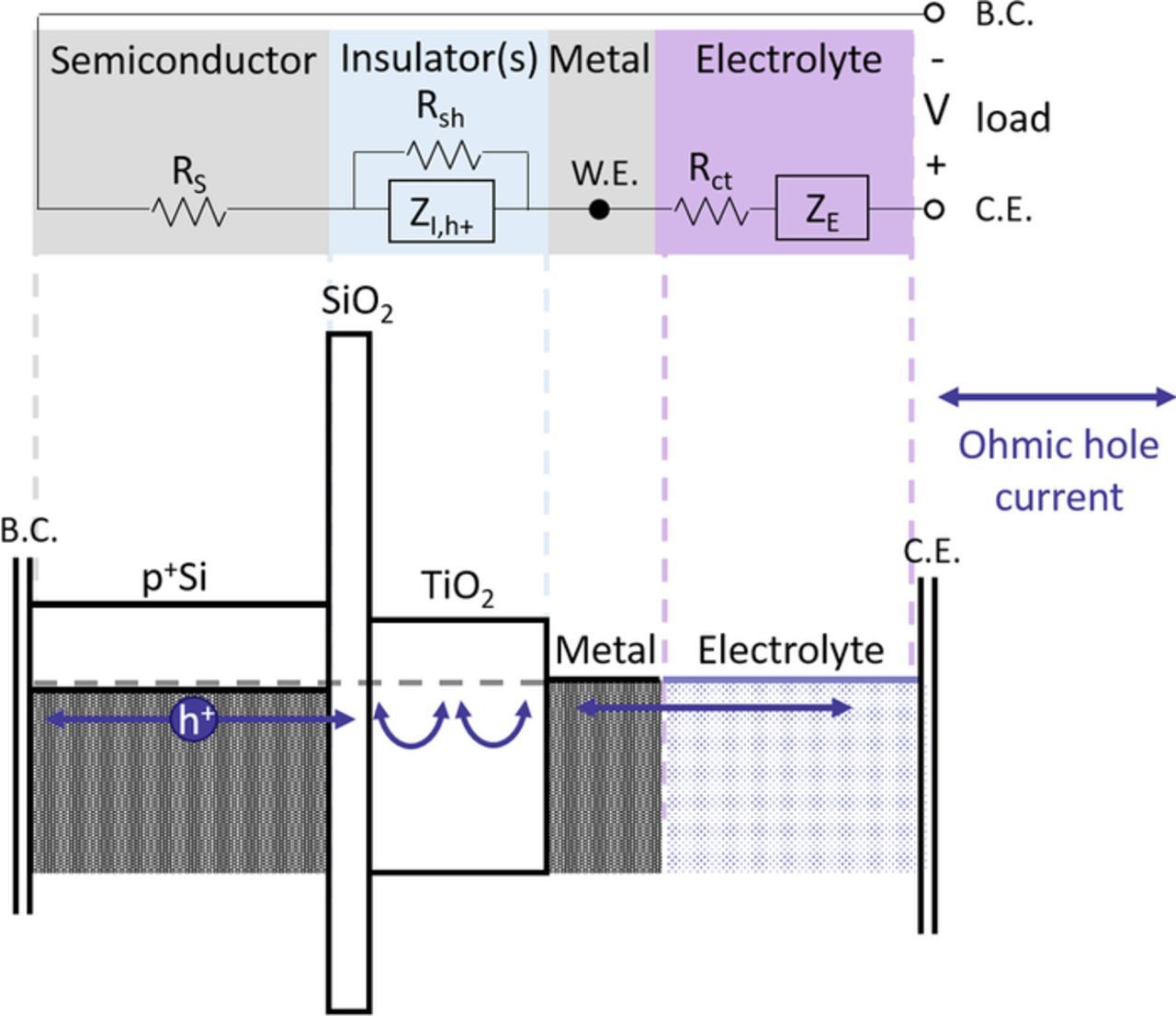
Figure 1. Band diagram of p+Si/SiO2/TiO2/Metal/Electrolyte overlaid with an equivalent circuit diagram, illustrating the current pathway and potential voltage losses in the device. In the equivalent circuit, RS is the series resistance of semiconductor, back side contact (B.C.), and wires, Rsh is a shunt path through the oxide, ZI,h+ is the non-shunted impedance through the oxide, in this case tunneling through SiO2 and trap-mediated conduction in TiO2, W.E. is the working electrode (the metal surface in electrochemistry), Rct is the charge transfer resistance from the solid-state anode to the electrolyte, ZE is the impedance of the electrolyte and C.E. denotes the counter electrode, in this case a platinum wire whose impedance contribution is, in practice, subtracted by three-electrode measurement.
Majority holes may encounter some series resistance internal to the semiconductor as well as external resistances (back side contact, wires, instrument resistance, etc.) denoted here as RS. In the insulator-stack, two pathways are depicted, namely a shunt pathway Rsh for the possibility of filamentary or pinhole-mediated conduction and a general impedance ZI,h+, which will depend on the insulator's properties. In this particular system, research has shown that the conduction mechanism through the SiO2 is a tunneling process5,9 and through TiO2 films greater than ∼2 nm thickness is bulk, trap-mediated conduction.6,7 In principle, for n number of distinct insulator layers in the stack and k parallel conduction pathways, there are nk permutations of conduction mechanisms. With two pathways and a bilayer insulator (e.g. SiO2/TiO2), there are four permutations: both insulator layers shunted, neither shunted, one, or the other shunted. Physically, shunting through both insulators in this bilayer or through the TiO2 layer only are the most probable outcomes for shunt conduction. Therefore we will consider a possible shunt (for instance due to metal filaments) across the entire insulator stack. A similar simplification cannot be made for the impedance ZI,h+ which we believe6 to be trap-mediated leakage conduction in parallel with a layer capacitance across the TiO2 layer and tunneling conduction in parallel with a layer capacitance across the SiO2 layer in Figure 1. Recent work has indicated that the two insulators interact in such a way that limited bulk conduction in the TiO2 may decrease the injection efficiency across the SiO2 into the TiO2.10 Equivalently, a thinner SiO2 may increase the efficiency of tunneling into traps beyond the interface with TiO2.
Figure 2 shows typical cyclic voltammetry results with a p+Si/SiO2/TiO2/Metal/Electrolyte half-cell measured using the reversible ferri/ferrocyanide redox couple in 1 M KCl(aq). An increase in insulator impedance is observed as an increase of the peak-to-peak splitting of the cyclic voltammograms. This system provides a valuable case study to investigate the different circuit components and their ultimate effects on photovoltage.

Figure 2. Ferri/ferrocyanide reversible redox cyclic voltammograms for p+Si/SiO2/TiO2/Metal/Electrolyte measured in the dark for five different TiO2 thicknesses increasing from black to orange to green to blue. The metal is iridium and the reversible redox couple is 10mM ferri/ferrocyanide 1M KCl. Both reductive and oxidative currents leading to the peak cathodic voltage Epc and peak anodic voltage Epa are functions of hole current in the device. Data were obtained at 100 mV/s scan rate with a 0.196 cm2 surface area.
From the equivalent circuit diagram, we can express Ohm's law for the redox reaction of Figure 2 with a p+Si anode as:
![Equation ([1])](https://content.cld.iop.org/journals/1945-7111/163/3/H192/revision1/d0001.gif)
where the voltage is referenced to the reversible redox potential E0 for the ferri/ferrocyanide couple (FFC) and experiences potential losses due to series resistance RS, shunt resistance Rsh, the insulator impedance ZI,h+, the charge transfer resistance at the electrolyte interface Rct and the electrolyte impedance ZE respectively. Ultimately, all of these elements must be understood and optimized. When focusing on the anode half-cell, a reference electrode is typically placed close to the working electrode (W.E.) to remove voltage drops elsewhere in the cell including all contributions of the counter electrode and the electrolyte impedance between the reference and counter. The electrolyte resistance remaining between the reference and the working electrode (a component of ZE), is known as the uncompensated series resistance (Ru) and, while minimal in many cells, can be quite significant in others, particularly if low conductivity solutions are required. As needed, electrochemical impedance spectroscopy (EIS) can be used to determine the uncompensated resistance and subtract its effects. An EIS correction can also remove any additional series resistance from the electrode structure, assuming the various layers are non-interacting. Such corrections allow for a great simplification of Equation 1. Assuming negligible shunting of current, leaves only the insulator impedance and the depletion impedance of the solution due to diffusion limitations which results in a voltage offset, Ediff, which is responsible for the peak shape:
![Equation ([2])](https://content.cld.iop.org/journals/1945-7111/163/3/H192/revision1/d0002.gif)
Two quantities are commonly extracted from reversible redox cyclic voltammograms such as those in Figure 2: the E1/2 (the average of the peak positions, a good approximation of the zero-current potential) and the peak-to-peak splitting (from which the DC resistance in  can be determined). From the solar cell perspective, it is the zero-current potential, or open-circuit photovoltage, and the DC resistance that are of interest while, from the electrochemical perspective, the E1/2 and peak to peak splitting are common metrics. Important differences can arise, however, between the values of these parameters from either solar cell or electrochemical measurements of the same anode structure, depending on the symmetry or asymmetry of the reduction and oxidation conduction pathways. For the p+Si case, conduction is essentially symmetric, representing majority holes from the semiconductor combining with electrons from the Ir or holes being created in the semiconductor as electrons are injected into the Ir. Figure 2 reflects this symmetry at positive and negative potential about the zero-current point. The potentials of the peak currents, Epa and Epc, can be obtained from Equation 2. The peaks are displaced from E0FFC by
  plus a diffusional splitting from the depletion offset potential,Ediff, which has a value of ∼29 mV for the one-electron ferri/ferrocyanide couple at room temperature.11 The peak to peak splitting (P2P) and half peak potential are given in Equations 3 and 4:
![Equation ([3])](https://content.cld.iop.org/journals/1945-7111/163/3/H192/revision1/d0003.gif)
![Equation ([4])](https://content.cld.iop.org/journals/1945-7111/163/3/H192/revision1/d0004.gif)
In this case, the E1/2 is approximately equal to the reversible redox potential and zero-current potential. The DC device resistance can also be exactly measured either by modelling the peak-to-peak behavior with electrochemical simulation software or by vigorously stirring the solution and making short, rapid potential sweeps to obtain non-diffusion limited current measurements. In the limit of perfect mixing, the slope at the zero-current potential also provides a measure of ZI,h+. In the case of a complex and significant impedance inconsistent with a linear series resistance, a more sophisticated computational model is needed to quantify the impedances. The best performing devices, however, often have low overall resistance, making the simple linear model generally applicable. The simple relationships of Equations 3 and 4 are useful to help clarify the more complicated relationships inherent in the minority-carrier photoanode devices.
The nSi Type 1 photoanode
The simplest possible photoanode structure consists of a single semiconductor layer capable of forming an electrochemical junction with the electrolyte, remaining stable itself, and even catalyzing the reaction. These Type 0 structures have been studied extensively in the literature in part because of the attractiveness of a simple architecture. Unfortunately, the underlying physical properties that control corrosion stability and photovoltaic efficiency of semiconductors are linked, such that Type 0 structures do not generally achieve stable and efficient solar-driven electrolysis.5,7 The protection layers discussed herein and reported in the literature have permitted the use of highly efficient photovoltaic materials with enhanced stability that allow for the advancement of solar fuel and solar chemical technology. The simplest thin insulator-protected structure that achieves high efficiencies and stabilities as a photoanode is the nSi/SiO2/TiO2/Metal device utilizing TiO2 for protection and the surface metal layer as both an OER catalyst and a contact for the resulting Schottky junction. The Schottky junction with nSi splits photogenerated electron-hole pairs, providing the holes needed for water oxidation. Figure 3 shows the band diagram and equivalent circuit diagram for the Type 1 nSi photoanode similar to Figure 1 for the reference p+Si anode.
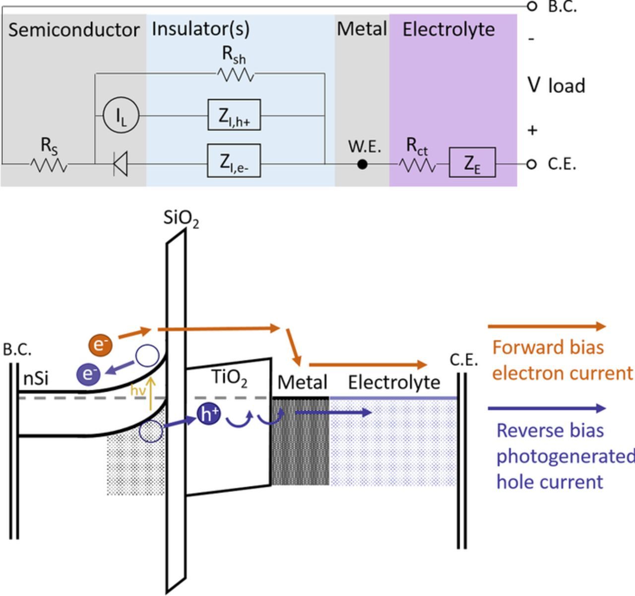
Figure 3. Band diagram of the Type 1 photoanode nSi/SiO2/TiO2/Metal/Electrolyte overlaid with an equivalent circuit diagram illustrating the current pathway and potential voltage losses in the device. The forward bias electron current experiences an impedance ZI,e- due to electron tunneling into the TiO2 conduction band and then band conduction from there into the metal. The reverse bias minority hole current experiences a different impedance ZI,h+ due to hole tunneling into trap states in the TiO2 and trap-mediated conduction to the metal. This pathway has been proposed based on reported experimental results4,5,9 for the TiO2-thickness and temperature dependence of ZI,h+.
In this case, there are two different impedances ZI,e- for electrons that can move via the TiO2 conduction band and ZI,h+ for holes that traverse the TiO2 via states in the bandgap. Possible shunt current paths will have a much greater impact on holes under reverse bias than on electrons under forward bias in this structure. This is a typical Schottky structure, so the junction is rectifying in the dark, blocking electrons from moving from the metal into the semiconductor. A shunt through the insulator layers would presumably not affect this pathway unless it also formed an Ohmic contact to the semiconductor, eliminating the band bending of the Schottky junction locally.
Figure 4 shows ferri/ferrocyanide cyclic voltammetry data from Type 1 nSi devices where increasing impedance increases the peak-to-peak splitting, but the effect is asymmetric. The anodic hole current experiences a greater penalty than the reductive electron current. Comparison to the data collected from p+Si anodes in the dark (Fig. 2) indicates that this behavior is consistent with a TiO2-thickness dependent photovoltage loss, as we describe in great detail in another report.7
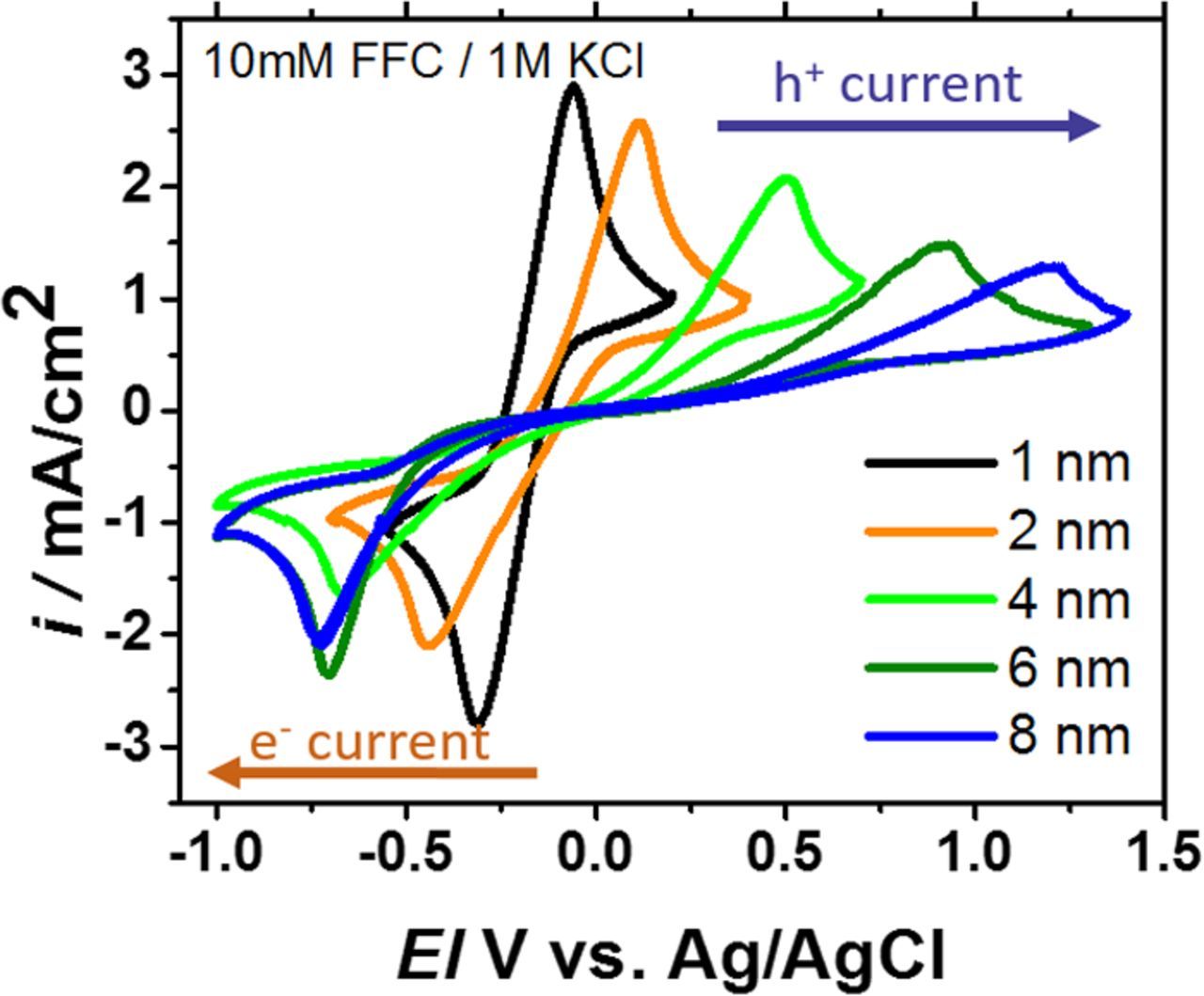
Figure 4. Ferri/ferrocyanide reversible redox cyclic voltammograms for nSi/SiO2/TiO2/Metal/Electrolyte anodes at 1 sun illumination with five different TiO2 thicknesses. The metal is iridium and the reversible redox couple is 10 mM ferri/ferrocyanide 1M KCl. Like the p+Si case, the peak-to-peak splitting increases with increasing TiO2 impedance (in color order), but the effect is asymmetric having much more impact on the anodic hole current than the reductive electron current. These data are obtained at 100 mV/s scan rate with a 0.196 cm2 surface area.
To describe this effect, the hole impedance is expressed as two terms, IRI,h+ to describe the linear series resistance loss that is also encountered in the p+Si reference sample with majority holes, and Eextraction-loss, a charge extraction loss that describes increased recombination in the junction of the nSi Schottky device as a result of insulator-impedance and is not seen in the p+Si reference sample. With these two terms as variables and considering the open-circuit photovoltage EOC as a constant, Equation 2 becomes:
![Equation ([5])](https://content.cld.iop.org/journals/1945-7111/163/3/H192/revision1/d0005.gif)
The peak anodic current Epa will include the diffusion splitting described above, the charge extraction loss Eextraction-loss, and the IR loss from the hole pathway depicted in Figure 3. The peak cathodic current Epc will now differ, not including any charge extraction loss, and including an IR loss from the electron pathway of Figure 3 instead. Considering these factors, the equations for peak-to-peak splitting and half peak potential are now:
![Equation ([6])](https://content.cld.iop.org/journals/1945-7111/163/3/H192/revision1/d0006.gif)
![Equation ([7])](https://content.cld.iop.org/journals/1945-7111/163/3/H192/revision1/d0007.gif)
The charge extraction photovoltage loss has been described in detail in other work.7 The loss can be understood via Gauss' Law as the need to sustain a certain charge density on the semiconductor-insulator interface in order to set the field at the surface of the semiconductor, which in turn determines the fields in the insulators, and, from that, the current density sustained across the insulator. The Eextraction-loss term scales linearly with the thickness of the insulator and can be related to the dielectric constants of the protective layers such that low-k SiO2 incurs a much higher loss than higher-k materials such as Al2O3 and TiO2. Importantly for this work, Eextraction-loss is a function of the current density (greater hole accumulation at the semiconductor surface is required to achieve higher current across a leaky capacitor), meaning that the photovoltage will no longer be equal to the open-circuit photovoltage at any arbitrary current density but will instead be a decreasing function of current density as referenced to the p+Si device. By extension, the E1/2 measured by reversible redox chemistry does not correspond to the EOC nor does the EP2P directly correspond to the hole impedance. Equation 6 and 7 differentiate the effects of the oxidative and reductive current for reversible redox and can be used to understand the photovoltage in those systems and in water oxidation half-cells.
The p+nSi type 2 photoanode
Recent work has shown that a buried p+n junction can decrease or even eliminate the charge extraction loss for more resistive oxides by sustaining a high hole concentration at the semiconductor/oxide interface.7,10 In this case, the only difference between the p+nSi photoanode and the p+Si anode reference will be the difference between hole and electron transport pathways affecting the reductive forward bias, as shown in Figure 5. For anodic operation, the two are now essentially identical.
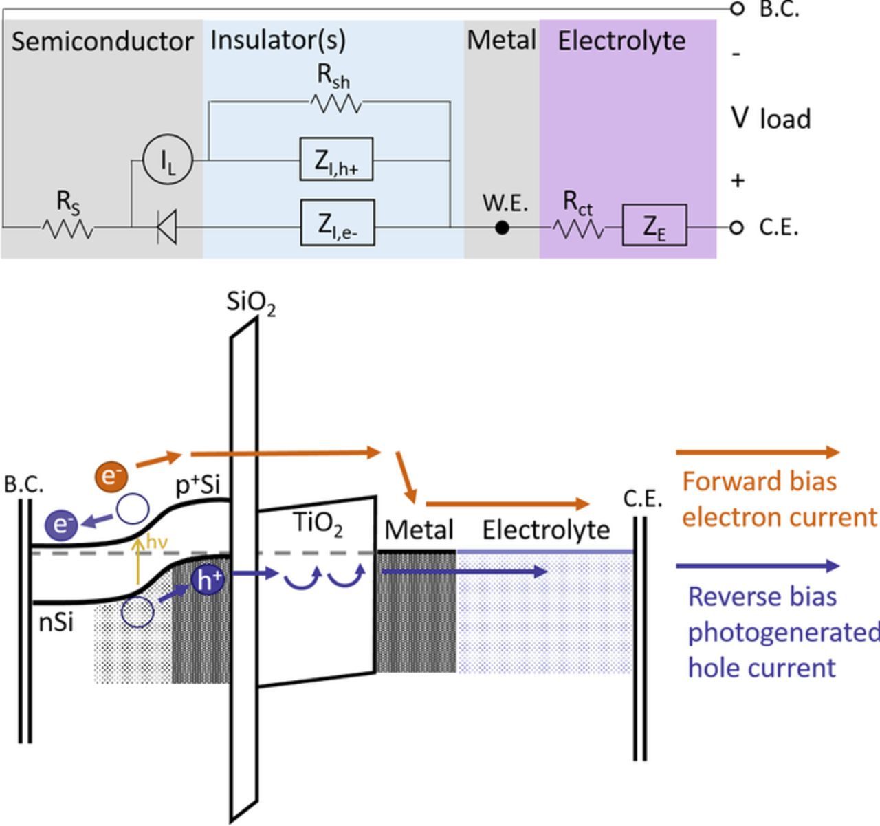
Figure 5. Band diagram of the Type 2 photoanode p+nSi/SiO2/TiO2/Metal/Electrolyte overlaid with an equivalent circuit diagram illustrating the current pathway and potential voltage losses in the device. The equivalent circuit diagram is equivalent to the Type 1 case, except that the oxide shunt pathway terminates in the p+Si, not affecting the diode. Most importantly for charge extraction, the p+ region at the interface ensures that the interface hole concentration stays high, incurring no charge extraction loss in these devices.
Considering these factors, the equations for peak-to-peak splitting and half-peak potential are identical to those for the nSi case, but without the charge extraction loss:
![Equation ([8])](https://content.cld.iop.org/journals/1945-7111/163/3/H192/revision1/d0008.gif)
![Equation ([9])](https://content.cld.iop.org/journals/1945-7111/163/3/H192/revision1/d0009.gif)
Figure 6 shows example cyclic voltammograms of the Type 2 device measured in the reversible redox couple ferri/ferrocyanide. As seen in Figure 6, the asymmetry of Figure 4 is completely removed and the curves trend almost identically to the p+Si reference case. This indicates that there are no significant differences in the forward and reverse bias current on the device. In terms of the equivalent circuit diagram, it suggests that the two impedances can actually be combined and treated as a simple resistor in series with the diode. The peak to peak splitting is therefore the same as the p+Si case and the E1/2 = E0FFC – EOC, which is the same as the p+Si case as well, shifted only by the constant open-circuit photovoltage. This simplification should hold true as long as the conduction across the insulator layers is fully decoupled from charge extraction from the junction. In the limits of either a very thin degenerately doped surface region or a very thick and resistive insulator, this assumption breaks down and the charge extraction penalty will still be significant. Another recent report has shown that, with ALD-Al2O3, a similar p+n buried junction greatly reduces the charge extraction penalty but does not remove it completely. This is likely attributable to the high resistance of the thicker Al2O3 films.10
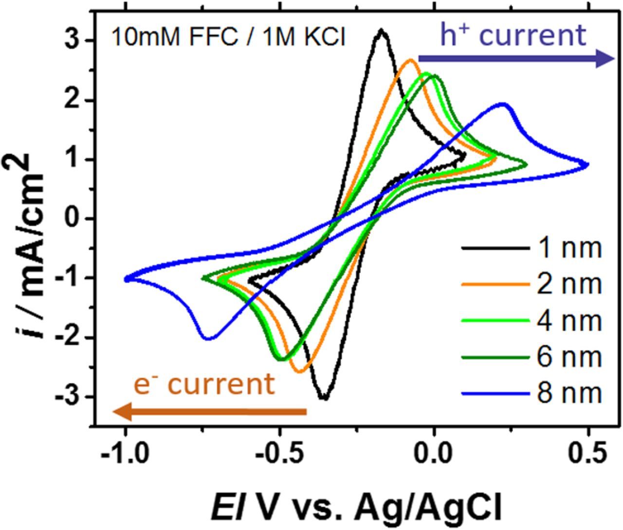
Figure 6. Ferri/ferrocyanide reversible redox cyclic voltammograms for p+nSi/SiO2/TiO2/Metal/Electrolyte measured under 1 sun of illumination for five different TiO2 thicknesses. The metal is iridium and the reversible redox couple is 10mM ferri/ferrocyanide 1M KCl as before. Like the p+Si and nSi case, the peak to peak splitting increases with increasing TiO2 impedance (in color order). Unlike in the nSi case, where the insulator caused increased recombination, in Type 2 photoanodes, the insulator only adds a series resistance, similar to the dark p+Si anode case. The photovoltage is large (550 to >600 mV) and constant for all device impedances in the study. These data are obtained at 100 mV/s scan rate with a 0.196 cm2 surface area.
Photovoltages measured for a reversible redox couple compared to photovoltage measured for water oxidation
Photovoltage in a half-cell is always defined relative to some reference. In some cases, that reference can be a constant, for example the reversible redox potential of an electrolyte species, E0, or the thermodynamic water oxidation or reduction potential. In other cases, reference samples or devices have also been used such as the p+Si dark anode described above in this paper or the noble metal catalyst or ideal fuel cell reported in the work of Heller.2 Measurement of the photovoltage at zero current, or the open-circuit voltage, can be directly carried out in a redox solution with a well-defined potential by simply measuring the voltage across the device at zero current. Most potentiostats can perform these measurements automatically and they can also be done with an independent voltmeter contacting the working and reference electrodes. In this section, the photovoltage will be explored relative to the p+Si dark anode. This allows for determination of photovoltage in a solution without a well-defined redox potential. Furthermore, it provides a well quantified system to explore the device performance as a function of current density identifying any successive losses, such as the Eextraction-loss mentioned above. By contrast in the discussion section, leading results reported from different groups will be compared using the voltage of the photoelectrode relative to a constant, thermodynamic reference because this is most effective for comparing results across different device types and experimentally incorporates the catalyst overpotential, which is an important loss for practical water-splitting devices.
Referring once again to cyclic voltammetry, the photovoltage shift for a reversible-redox couple can, in principle, be taken as the zero-current point of the photoanode measurement relative to the zero-current point of the p+Si dark anode, which is also the E1/2 for p+Si, the reversible redox potential described in the prior section. This approach is ideal for measuring open-circuit photovoltage. In relatively conductive cells, this measurement can be done without difficulty; however, in cells with a higher impedance, the current-voltage relationship is generally non-linear and the current remains near zero over an extended range of voltage. Considering Figure 4, it can be seen that the zero-current point seems to move to the right with increasing TiO2 thickness, while the difference in voltage from curve to curve at higher current densities changes more rapidly. The same effect can also be observed in the water oxidation measurements for this particular kind of loss and is characteristic of a charge extraction barrier. By subtracting Equation 4 from Equation 7, we obtain a different, and more easily measured photovoltage. This difference between the E1/2 values for the Type 1 nSi photoanode and reference p+Si systems is:
![Equation ([10])](https://content.cld.iop.org/journals/1945-7111/163/3/H192/revision1/d0010.gif)
Equation 10 indicates that the half-peak potential shift equals the open circuit photovoltage modified by a term comparing the relative impedances of the hole and electron pathway through the structure and half of the charge extraction loss. This equation represents an averaging of forward and backward electrochemical reactions at the anode. With the terms delineated in this way, it can be directly compared to the shift of the water oxidation reaction. In this case, the overpotential shift between the Type 1 nSi photoanode and a reference p+Si anode for the water oxidation reaction at given current densities (potentials EI) can be written as:
![Equation ([11])](https://content.cld.iop.org/journals/1945-7111/163/3/H192/revision1/d0011.gif)
![Equation ([12])](https://content.cld.iop.org/journals/1945-7111/163/3/H192/revision1/d0012.gif)
![Equation ([13])](https://content.cld.iop.org/journals/1945-7111/163/3/H192/revision1/d0013.gif)
Equation 12 shows that the water oxidation overpotential is a function of the thermodynamic water oxidation potential E0O2/H2O, a Nernstian term dependent on O2 partial pressure and pH, the activation overpotential which is a function of the catalyst-reaction relation, and an impedance loss from hole conduction through the structure. The photoanode is only different from the reference anode in the photogenerated minority holes which gives the photovoltage. Because no averaging of forward and backward reactions is being done, the result is the open-circuit photovoltage and the full charge extraction loss remains, unlike in the reversible redox case.
Photovoltage relation measured for the water oxidation half-cell and reversible redox couple for impedance scaling
In many of the studies reported recently, the insulator impedance has been systematically varied by changing the thickness of one or more insulator layers in oxide-protected photoelectrodes. Impedance can also be varied in other ways, for example by doping, post-deposition treatments, microstructure changes, or by controlling the shunt path density. For all such studies, it is useful to know the relationship between Equation 10 and 13 above, the reversible redox couple E1/2 shift and a half-cell water oxidation shift. This can be accomplished by taking partial derivatives with respect to the factor that is systematically varied to control impedance. In recent studies, this factor has been the insulator thickness. In this section, it is assumed that the open-circuit voltage is independent of the hole conduction impedance ZI,h+, and that the Eextraction-loss term, which only affects holes in photoanode operation, can represent all photovoltage loss with respect to changes in ZI,h+. Previous work on MIS solar cells has shown that the EOC does in fact decrease linearly with the thickness of the insulator layer,12 but that effect, measured with ultrathin oxides explicitly, was much smaller than the current-dependent Eextraction-loss seen here with thicker oxides. With this assumption of constant EOC, the partial derivatives of the E1/2 shift and half reaction overpotential shifts with respect to insulator thickness ti are:
![Equation ([14])](https://content.cld.iop.org/journals/1945-7111/163/3/H192/revision1/d0014.gif)
![Equation ([15])](https://content.cld.iop.org/journals/1945-7111/163/3/H192/revision1/d0015.gif)
If the two values on the left hand sides of Equations 14 and 15 are measured at the same current density, the Eextraction-loss is identical, producing a relation between the two shifts:
![Equation ([16])](https://content.cld.iop.org/journals/1945-7111/163/3/H192/revision1/d0016.gif)
Equation 16 indicates that the E1/2 shift is half of the water oxidation overpotential shift measured in the half-cell adjusted for half the impact of any difference in hole and electron conductivity in the structure. To gain some quantitative insight into this analytical model, Table I lists values of the E1/2 trend with TiO2 thickness (peak currents 1–2 mA/cm2) and half of the water oxidation overpotential shift (at 1 mA/cm2) for varying TiO2 thickness in three sets of anodes with SiO2/TiO2/Metal over the indicated substrate type where the metal used is iridium as before. All sets show bulk-limited conduction in which a constant field is required across the TiO2 to drive a constant current; however, the absolute magnitude of the required field is different by about a factor of three between the 'more' and 'less' conductive set. Such changes in insulator conductivity at the same nominal thickness indicate variations in the TiO2 trap and/or shunt path density. A comparison between the two shifts and any residual difference between the values in reference to Equation 16 shows a similar relationship for both Type 1 sets at presumably different TiO2 resistivities.
Table I. E1/2 and ½ OP shift comparisons for two TiO2 protected sets with different TiO2 resistivity.
| Photoanode |  |
 |
Residual |
|---|---|---|---|
| sets | (mV/nm) | (mV/nm) | (mV/nm) |
| Type 1 nSi (more conductive) | −20.7 | −24.3 | +3.6 |
| Type 1 nSi (less conductive) | −54.0 | −49.7 | −4.3 |
| Type 2 p+nSi (less conductive) | ∼0 | ∼0 | ∼0 |
The residual is the difference between the E1/2 shift and half of the water oxidation overpotential shift. According to Equation 16 this should be equal to half of the difference in resistance scaling between the electron and hole pathway through the device. The two values from the Type 1 nSi devices, +3.6 mV/nm and −4.3 mV/nm suggest a very small difference in contributed resistance for the two carrier pathways. Further evidence comes from the Type 2 p+nSi devices with less conductive TiO2. The residual is approximately zero (0.3 mV/nm) in the situation where the charge extraction loss should be completely removed and the photovoltage is approximately constant with respect to insulator thickness. In the previous section it was assumed that only a charge extraction loss affects the anodic current in comparing ferri-ferrocyanide redox data and water oxidation overpotential data from identical anode structures. The data in Table I are consistent with Equation 16, supporting the conclusion that the charge extraction loss occurs when the insulator is placed inside the junction across which photogenerated electrons and holes are separated (i.e. Type 1 anodes).
Discussion
Power metrics to compare water-splitting device performance
The previous sections defined the photovoltage in insulator-protected photoanodes referenced to p+Si reference anodes. Those sections also examined common electrochemical metrics, the peak-to-peak splitting and half-peak potential in cyclic voltammetry using standard redox couples and how they are related to the photovoltage. In this final discussion, notable results from water-splitting photocathodes and photoanodes will be investigated and directly compared by presenting a power metric relative to the thermodynamic potential of water reduction or oxidation respectively. This analysis assumes that a useful water-splitting cell will be composed of both a photoanode and a photocathode in order to generate a large enough photovoltage to drive water-splitting. The voltage needed to drive a device-relevant current density, such as 10 mA/cm2, across the whole water splitting cell will include the thermodynamic potential of water-splitting 1.229 V as well as activation overpotentials for each half reaction, series resistance losses to reach the required current density, solution losses, product separation losses and more. Literature results are typically carried out with a three electrode setup and some also subtract the uncompensated series resistance. So the voltage required to reach 10 mA/cm2 does not yet account for many of the losses. The solution resistance, for example, would easily contribute ten or more ohms requiring another 100 mV or more at 10 mA/cm2. Highly acidic solutions tend to be the most conductive, so results in acid will likely require less additional potential to overcome the solution loss.
Tables II and III present a selection of recent results for water reduction cathodes and water oxidation anodes, specifically listing those that involve some form of semiconductor corrosion protection layer, either using insulators or metals (catalysts). Most reports describe multiple electrode structures, so effort was taken to select the best results from each type, but also to add notes about the context for that result. Power producing half-cells are listed as having a positive photovoltage relative to the reversible potential, whereas power losing half-cells are listed as having a negative photovoltage relative to the reversible potential. All values are given relative to the hydrogen evolution thermodynamic potential (for cathodes) and oxygen evolution potential (for anodes). The next column lists the photovoltage needed from the other half-cell to provide the minimum 1.229 V needed. There are several advantages and disadvantages to listing the data in this way. The catalyst choice, loading, surface area, and other catalyst parameters play a large role in both HER and OER activity and it is possible certain approaches are quite promising in stability and/or open-circuit voltage, while being poor in catalysis, for example the 2015 result from Mei that used Pt as a demonstration of a non-nickel high work function metal.13 More importantly as a disadvantage, these two tables do not include all the losses mentioned above meaning they represent underestimations of the voltage needed. Chief among the advantages of such a listing is the comparison of the power at a possible operating point i.e. for the voltage needed at 10 mA/cm2 operating current density. Looking at the photovoltage needed from the other half-cell indicates where today's research efforts are with respect to realizing an unassisted, stable, and efficient water splitting device.
Table II. Power metrics for protected water-reduction photocathodes at 10 mA/cm2.
| Year | Authors | Device structure | Photovoltage vs E0H2/H2O (Power producing is positive) | Photovoltage needed from anode | Notes |
|---|---|---|---|---|---|
| 2011 | Paracchino24 | Pt/TiO2/Al-ZnO/Cu2O | ∼0 (pH 4.9) *actually achieves only 7.8 mA/cm2 | ∼1.23 (pH 4.9) | -Moderate to poor stability 20 min, but great improvement from no protection |
| 2013 | Dasgupta25 | Pt/TiO2/pSi core-shell | +0.106 (pH 0.3) | 1.123 (pH 0.3) | -Highest Pt loading (10x) -1 hr stability |
| 2013 | Esposito15 | Pt/Ti/pSi | +0.093 (pH 0.3) | 1.136V (pH 0.3) | -Thick Ti, regrown SiO2 -2hrs stable -Inversion layer, H2 spillover effects |
| 2013 | Lin26 | Pt/TiO2/n-i-p aSi /ZnO | +0.582 (pH 4) | 0.647 (pH 4) | -Amorphous Si p-i-n structure -More losses expected from solution resistance |
| 2014 | Feng16 | Ni/Ti/pSi Pt NPs /Ni/Ti/pSi | −0.070 (pH 14) +0.200 (pH 14) | 1.299 (pH 14) 1.029 (pH 14) | -Stability poor -Good stability in pH 9.5 K/Li-borate, but loses 250 mV |
| 2014 | Kast17 | Pt/TiO2/F:SnO2/Ti/n+pSi | +0.523 (pH 0.3) | 0.706 (pH 0.3) | -Commercial pn Si junction with TiO2 protection and Pt |
| 2015 | Ji27 | Pt/Ti/SrTiO3/pSi | +0.100 (pH 0.3) | 1.129 (pH 0.3) | -8 unit cells of protection is best -35hrs stable |
| 2015 | Lai28 | Ni/Ti/pSi | −0.035 (pH 9.2) | 1.264 (pH 9.2) | -More losses expected due to solution resistance -4hrs stable |
| 2015 | Li29 | ALD-TiO2/Pt/pSiNW | −0.071 (pH 0.3) | 1.300 (pH 0.3) | -TiO2 deposited on top of catalyst -2hrs good stability in 0.5M H2SO4 |
| 2015 | Lin30 | TiO2/InP | +0.723 (pH 0.3) | 0.506 (pH 0.3) | -TiO2 decreased recombination |
Table III. Power metric for protected water-oxidation photoanodes at 10 mA/cm2.
| Year | Authors | Device structure | Photovoltage vs E0O2/H2O (Power producing is positive) | Photovoltage needed from cathode | Notes |
|---|---|---|---|---|---|
| 2011 | Chen, Prange5 | Ir/TiO2/nSi | −0.013V (pH 14) +0.075V (pH 0) | 1.242V (pH 14) 1.154V (pH 0) | -Ultrathin TiO2 tunnel oxide -8+ hr stability |
| 2013 | Strandwitz29 | MnOx/nSi | −0.062V (pH 14) | 1.291V (pH 14) | -Only 10 min of stability measured |
| 2013 | Kenney30 | Ni/nSi | +0.012V (pH 14) −0.189V (pH 9.5) | 1.217V (pH 14) 1.418V (pH 9.5) | -100+ hr stability at pH 9.5 with K-borate / Li-borate solution. -More losses expected from solution. |
| 2014 | Mei31 | IrOx/p+nSi | +0.034V (pH 0) | 1.195V (pH 14) | -18+ hr stability-Heating to 648 K gives extra 40 mV |
| 2014 | Mei32 | Fe-NiO/p+nSi | +0.067V* (pH 14) | 1.161V (pH 14) | -*Extra loss expected, iRS corrected -300hr stability, slight loss |
| 2014 | Hu8 | Ni/TiO2/nSi Ni/TiO2/p+nSi | −0.020V (pH 14) +0.020V (pH 14) | 1.249V (pH 14) 1.209V (pH 14) | -Very conductive, thick TiO2, 400 mV nSi, 520 mV p+nSi photovoltage-100+ hr stability |
| 2014 | Hu8 | Ni/TiO2/p+nGaAs | +0.424V (pH14) | 0.805V (pH 14) | -Thick, conductive TiO2 |
| 2014 | Hu8 | Ni/TiO2/nGaP | X (current too low) | X (current too low) | -Only reaches ∼4 mA/cm2 |
| 2014 | Lichterman33 | Ni/TiO2/nCdTe | +0.040V (pH 14) | 1.189V (pH 14) | -435 mV Voc for 1.5 eV bandgap CdTe |
| 2014 | McDowell34 Ho-Kimura35 | Ni/TiO2/BiVO4 BiVO4-TiO2 composite | X (current too low) | X (current too low) | -McDowell ∼2mA/cm2 Ho-Kimura ∼1mA/cm2 |
| 2015 | Mei13 | Pt/TiO2/Ti/p+nSi | −0.342V (pH 14) | 1.571V (pH 14) | -High conductivity w/ & w/o TiO2 -Pt used for demonstration |
| 2015 | Hill36 | CoOOH/Co/SiOx/nSi | +0.033V (pH 14) | 1.196V (pH 14) | -Simple electrodeposited contact, 470 mV photovoltage -But poor stability |
| 2015 | Chen37 | NiFe/NiCo2O4/p+nSi | +0.134V (pH 14) | 1.095V (pH 14) | -Good conductivity and voltage |
| 2015 | Scheuermann7 | Ir/TiO2/p+nSi | −0.012V (pH 14) +0.134V (pH 0) | 1.241V (pH 14) 1.095V (pH 0) | Thicker TiO2 for stability, still some insulator resistance, record photovoltage (630 mV) |
To illustrate, consider a tandem cell with semiconductors having bandgaps of 1.1 eV and 1.8 eV respectively.14 In this scenario, the 1.1 eV material (for example silicon) must likely provide over 600 mV of potential to combine with 1.1 V or more supplied by the larger bandgap semiconductor. The best pSi Schottky junction cathode results from Esposito15 and Feng16 achieve up to 500 mV photovoltages, while n+pSi junctions have achieved nearly 600 mV.17 For photoanodes, the most recent results7 achieve photovoltages as high as 630 mV with p+nSi and up to 550 mV with nSi, with somewhat resistive TiO2 protection layers. Reports in which the TiO2 resistance is greatly reduced have achieved photovoltages of 400 mV or less in many cases with nSi and 400 mV–520 mV with p+nSi.8 Several reported photoelectrodes were not included in the tables because their performance was either notably poorer than those listed or the results did not reach the required current density of 10 mA/cm2. For instance, hematite is a widely-studied photoanode material with a bandgap near 2.2 eV, but has yet to produce 10 mA/cm2 of photocurrent even when highly active iridium OER catalysts are used.18 MnOx is listed in this table as a passivation layer, but a recent report concludes that it is not well suited for such purposes.19 Work continues in developing it as an OER catalyst, but the best illuminated results reported imply negative potentials (power losing cells) of several hundred millivolts after accounting for the photovoltage. Protection layers including graphene or other carbon films have also been explored20–22 as has Ta2O5 as a protection layer for nZnO absorbers,23 but, in general produce worse results than those listed. Additional structures are also listed in a recent comprehensive review.4
Conclusions
In this report, the photovoltage at an operating current density of 10 mA/cm2 is analyzed as a device-relevant metric for water oxidation and reduction half-cells. The photovoltage and how to correctly measure it from typical electrochemical methods is discussed in detail for insulator-protected cells using Si/SiO2/ALD-TiO2/Metal anodes as a case study. A relationship is developed between the photovoltage derived from the half peak potential shift of the reversible ferri/ferrocyanide redox couple and the potential shift of water oxidation. Finally, numerous leading literature results are compared based on the photovoltage at 10 mA/cm2 photocurrent, referenced to the thermodynamic potential for hydrogen evolution (for cathodes) and oxygen evolution (for anodes), thus allowing for a direct comparison and indicating the importance of optimizing photovoltage in on-going research.
Acknowledgments
The authors acknowledge T. Carver for metal electron beam evaporation for the example anodes used. This work was partially supported by the Stanford Global Climate and Energy Project and a National Science Foundation award CBET-1336844. We acknowledge support from the Center for Integrated Systems and Precourt Institute for Energy seed grants. A.S. graciously acknowledges financial support from a Stanford Graduate Fellowship and a National Science Foundation Fellowship.