
Abstract
Electronic conductivity of battery electrodes and the interfacial resistance at the current collector are key metrics affecting cell performance. However, in many cases they have not been properly quantified because of the lack of a suitably accurate and convenient non-destructive measurement method. There are also indications that conductivity across deposited films is not uniformly distributed. To characterize these variations, a micro-four-line probe has been developed for local mesoscale measurement of electronic conductivity of thin-film electrodes. The micro-four-line probe, coupled with a previously discussed mathematical model, overcomes key limitations of traditional point probes. This new approach allows pressure-controlled surface measurements to determine electronic conductivity without removal of the current collector. In addition, the probe allows one to measure the local interfacial contact resistance between the electrode film and the current collector. The method was validated by comparing to other conductivity sampling methods for a conductive test film. Three commercial-quality Li-ion battery porous electrodes were also tested and conductivity maps were produced. The results show significant local conductivity variation in such electrodes on a millimeter length scale. This method is of value to battery manufacturers and researchers to better quantify sources of resistance and heterogeneity and to improve electrode quality.
Export citation and abstract BibTeX RIS

This is an open access article distributed under the terms of the Creative Commons Attribution Non-Commercial No Derivatives 4.0 License (CC BY-NC-ND, http://creativecommons.org/licenses/by-nc-nd/4.0/), which permits non-commercial reuse, distribution, and reproduction in any medium, provided the original work is not changed in any way and is properly cited. For permission for commercial reuse, please email: oa@electrochem.org.
A common electrode design for secondary batteries is a porous thin film of active material particles, conductive carbon particles, and polymeric binder. The film is coated on a metallic current collector. For commercially produced cells based on lithium-ion intercalation chemistry, the active materials are commonly a transition metal oxide on aluminum for the cathode and graphite on copper for the anode.
Among the key properties determining electrode performance are the volume-averaged (effective or bulk) electronic conductivity of the film and the interfacial resistance at the current collector.1–4 These two quantities are surprisingly difficult to measure accurately for common thin-film electrodes because of the relatively large contact resistance between the sample and external probes, mechanical fragility of the sample, and the presence of the attached current collector. Lack of experimental data makes it hard to meet a longstanding need to be able to predict these parameters from knowledge of the composition and structure of the constituent materials.
Commercial Li-ion battery electrodes are fabricated by first by making a slurry of the active material, carbon additive, binder, and a carrier solvent. This slurry is spread onto a metal foil current collector in a continuous process using a blade or slit to control deposition thickness, and then is immediately dried. Even in commercial coating processes it is difficult to achieve a uniform distribution of particles and porosity, leading to variability in the electronic conductivity of the electrodes.5 While this variability is generally accepted, little has been done to quantify it. It is important to understand this variability because it can lead to uneven currents and potentials in the electrode (so-called hot and cold spots), which inhibit optimal utilization of active material. Furthermore, such variability can accelerate degradation and failure mechanisms.
Prior research has been done to quantify the electronic conductivity of thin-film materials on multiple length scales, with varying levels of practicality for battery electrode films. Kerlau et al.6 and Ramdon and Bhushan7 have used current-sensing atomic force microscopy to establish the relative microscale conductivities of surfaces. While this has extremely high spatial resolution and imaging capability, it is less adapted to probing conductivity away from the surface particles and quantitative measurement is confounded by the large interfacial resistance between the probe tip and surface particles. Techniques that involve multiple probes have an advantage in that they may be able to correct for probe contact resistance. Perkins et al. have explored a microscale method for conductivity characterization using a multi-point probe in ultra-high vacuum.8 This has the advantage of high spatial resolution and positioning, but precise pressure control and microprobe breakage are issues with this technique. Previously, our group has measured bulk electrode conductivity by delaminating the electrode film from its current collector, attaching it to an insulating support surface, and pressing against a macroscale four-line probe.9
We note some prior work that purports to be able to deduce the contact resistance between the electrode film and the current collector.10,11 This is a potentially significant source of internal resistance in batteries,12 and it can be difficult to quantify separately from other resistances.
Our goal is to develop a rapid, accurate, and non-destructive method to measure these conductive properties. Recent work in a companion paper1 has demonstrated that a four-line contact geometry with line spacing on the order of the film thickness is ideal. The model allows for realistic boundary conditions and arbitrary geometry, and thus allows electrode samples to be analyzed without delamination from their current collectors, making nondestructive measurements possible. 2D and 3D versions of the model were reported. As the 3D model is more realistic, it was used for all analysis in this paper. As the prior paper indicates, we measure the electrical characteristics using two different electrical configurations, one in which current passes tangentially to the electrode surface and another in which current flows largely orthogonal to the surface, so that the model can accurately determine both electrical conductivity and contact resistance.
This paper presents the development of a micro-four-line probe (μ4LP) that can measure conductive properties over a sampling window of size  , thus giving μm-order lateral resolution for thin-film battery electrodes. The probe was validated and tested on four different samples. The first was a conductive silicone sheet that has a bulk conductivity similar to typical Li-ion battery electrodes. We find that the average conductivities are consistent with those obtained by other experimental methods. Next the probe was used to test two cathodes and one anode produced by Argonne National Laboratory. Furthermore, the measurement method based on the μ4LP allows for rapid scanning across the surface of planar electrodes, including making a conductivity map to assess local conductivity variability inherent in the fabrication process.
Probe and Fixture Design
A probe was fabricated using standard cleanroom procedures in the Brigham Young University cleanroom. In addition to the probe, a computer-controlled stage to move the probe to different locations on a sample was constructed. A summary of this experimental design is given in this section.
Probe geometry
To determine the physical dimensions of the μ4LP device, most importantly the width of and spacing between the lines, typical characteristics of Li-ion battery cathodes and anodes were considered: conductivity ranging from 10 − 1500 mS/cm (depending on the active material), thickness on the order of 30 − 100 μm (excluding the aluminum or copper current collector), and surface roughness around 5 μm (based on typical active material particle size). Surface roughness necessitates that the line widths and lengths be large enough to ensure consistent contact with the electrode. Moreover, the size and spacing of lines determines the volume that is sampled. It is desirable to sample a volume large enough to incorporate many particles at all depths so that a relatively small number of samples will be representative of the whole electrode. There is some flexibility in the design because the mathematical model takes into account the distribution of current for the actual probe and sample geometry.1 For instance, the model can show for a given geometry what fraction of the tangential current passes through the attached current collector. It was found that, as a general rule, the distance between the two outer lines of the probe should be approximately the same as the sample film thickness.1
With the above considerations in mind, the lines were designed to be 10 μm wide and 3 mm long, with  spacing between them, as shown in Fig. 1. In the design, voltage signals and current are carried from the four contact pads (shown at the bottom of Fig. 1 a) to the probing region by means of nickel layers deposited on an insulating wafer. The nickel layers are covered by an insulating polymer layer (blue in the figure) except for the contact pads and a
  sampling window. This window allows us to place the planar four-line probe on top of a film sample and only make the necessary electrical contact to the film in that region.
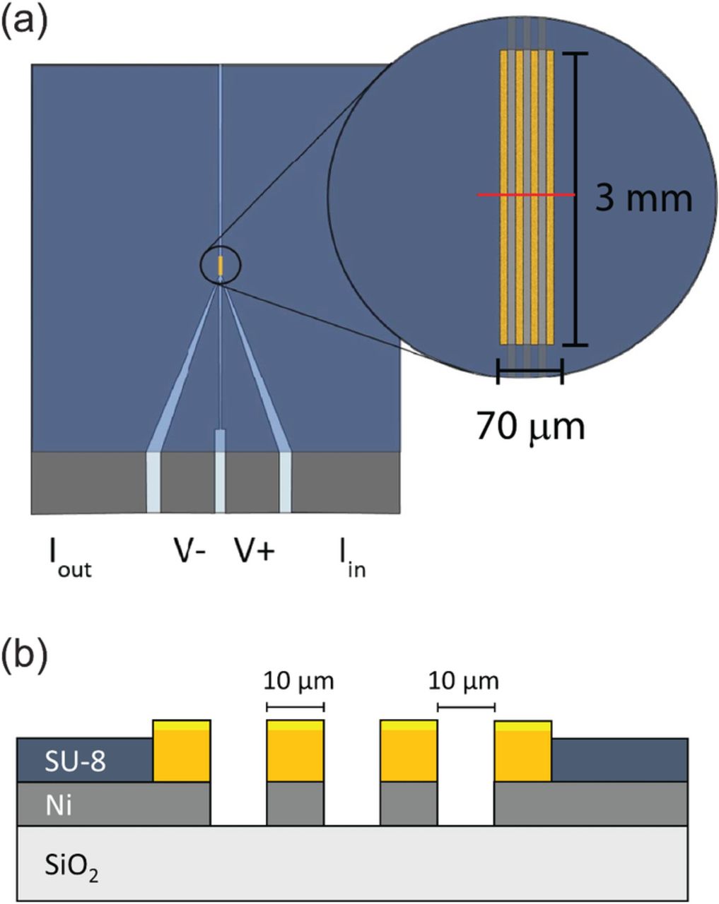
Figure 1. Design of device (not to scale): (a) as seen from above with magnified sampling window, (b) cross-sectional view of sampling window where contact with electrode film takes place.
Cleanroom fabrication and electrodeposition
The basic fabrication process steps used to produce the μ4LP are shown in Fig. 2. Fused silica wafers were used as substrates because they are flat, smooth, and offer near-perfect electrical insulation. AZ 2020 photoresist (AZ Electronic Materials USA, NJ, USA) was applied to the substrate and exposed on a Karl Suss MA150 aligner (Karl Suss America, VT, USA) before being developed. Next, a 150 nm film of nickel was deposited using a CHA-600 thermal evaporator (CHA Industries, CA, USA). The photoresist layer beneath the nickel was then removed using NMP, leaving four lines of nickel on the wafer. Following the lift-off, a 750 nm layer of SU-8 photoresist (Microchem Corporation, MA, USA) was applied as a protective layer that covered all but the  sampling window centered over the four lines and the pads to electrically connect to the lines. Upon completion, the wafers were diced into separate probes using a Disco Dad 320 Automatic Dicing Saw (DISCO Corporation, Tokyo, Japan). A completed device is shown in Fig. 3.
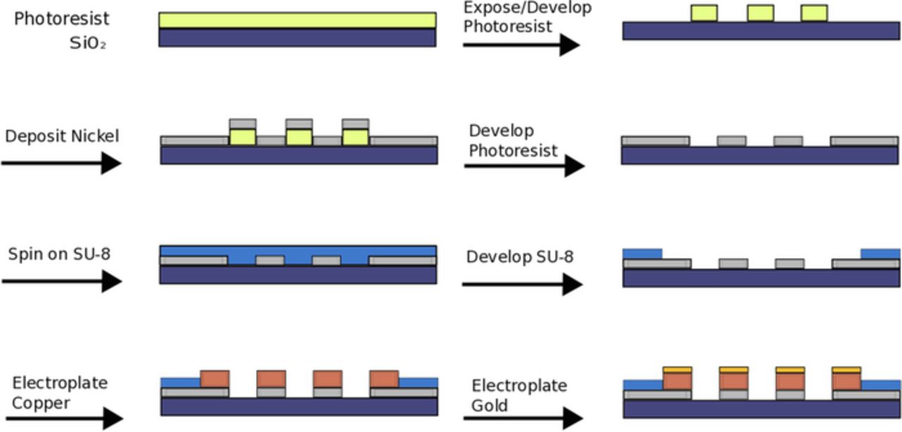
Figure 2. Cleanroom fabrication process to produce μ4LP. Shown is a cross-section view across the window over the four exposed lines.
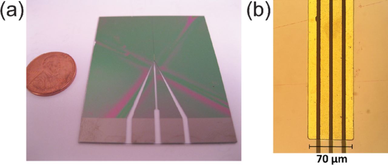
Figure 3. (a) Completed micro-four-line probe with a U.S. penny shown for comparison. (b) 200× magnified image of a portion of the window of exposed lines (light-colored regions).
After the device was fabricated in the clean room, electrodeposition was used to raise the height of the exposed lines close to 0.8 μm above the surrounding SU-8 polymer layer, facilitating surface contact with the sample film during measurement. The exposed CVD nickel layer was activated for plating with a typical nickel strike formulation (1.0M HCl and 3.5M NiCl2). After the nickel surface was prepared, it was electroplated with copper using an acidic solution (0.85M H2SO4 and 0.14M CuSO4) and a copper foil counter electrode with potential maintained 0.4 V above the line to be plated. Copper plating was continued until the desired amount of charge was passed. Final line heights were verified by a profilometer (Tencor Alpha-step 200). In order to protect the copper lines from oxidation, a thin layer of gold was plated on top using a stainless steel counter electrode with potential maintained 1.2 V above the line to be plated, using a standard cyanide-based gold-plating solution.13 The probe template was designed to yield 10 μm wide lines, but because of nearly isotropic electroplating on the sides as well as the tops of the lines, at the completion of the process the lines had widened to 12 μm.
Practical adaptation of mathematical model
As specified by the mathematical model,1 two different electrical configurations must be used with the μ4LP to estimate the bulk conductivity and interfacial resistance. The configurations are referred to as the tangential and orthogonal experiments. An underlying assumption in the model for both experiments is that the potential of the current collector is the reference plane at ground and that currents are injected and removed via electrodes at positive and negative voltages. In practice this is modified for the tangential experiment to allow a single-voltage supply to function for both types of experiment. The supply provides the current that is injected into the electrode material as shown in Fig. 4. Thus, in the tangential measurement the current collector is left floating at a potential intermediate to that of the applied voltage (one outer line) and ground (the other outer line). In the case of the orthogonal measurement, the current collector is grounded, as assumed in the model.
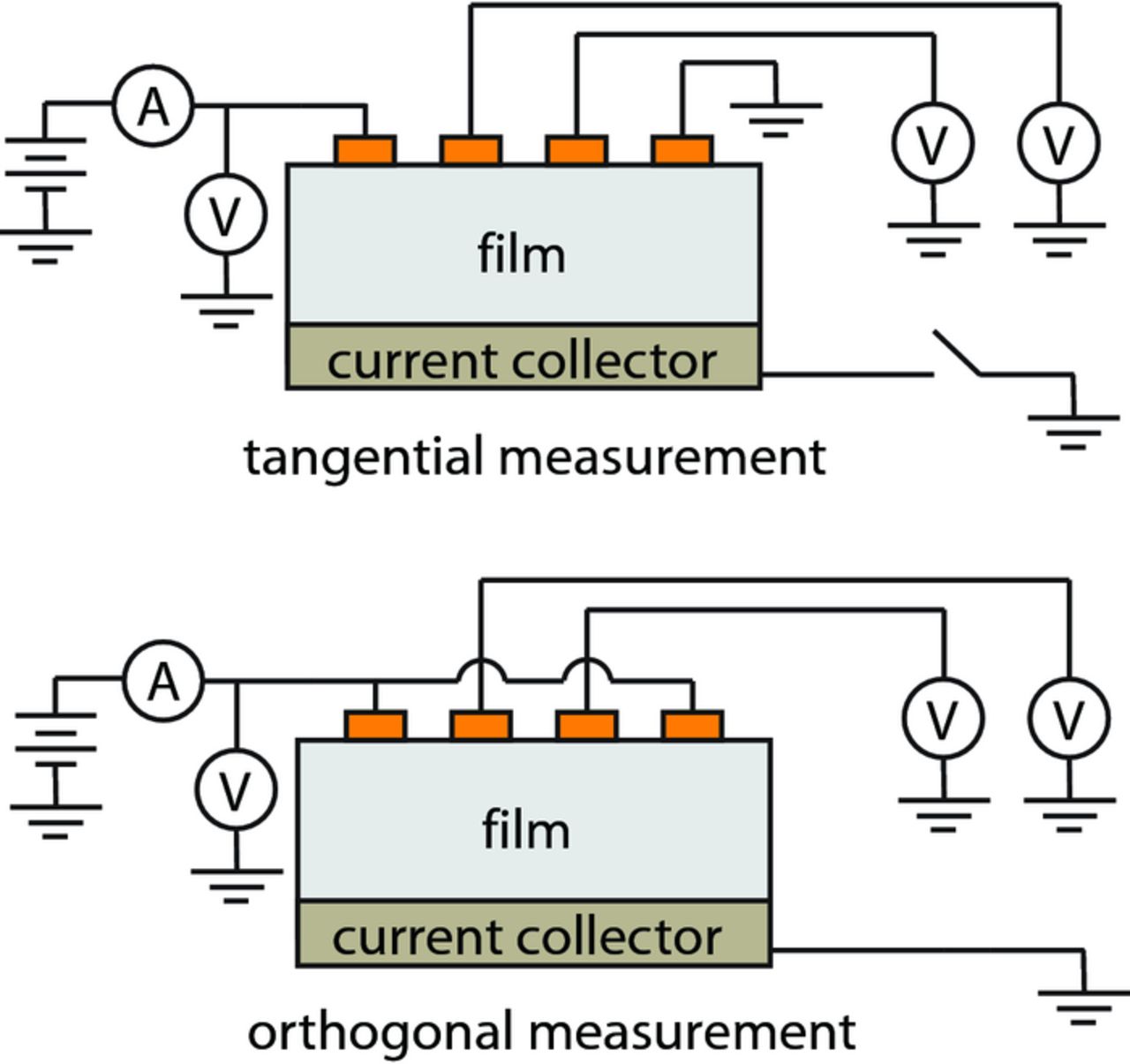
Figure 4. Electrical configurations to perform tangential and orthogonal measurements with the μ4LP. A relay is used to rapidly switch between the two configurations.
In addition, the model assumes perfect symmetry across the plane separating the two inner lines, while for real samples such symmetry is only approximate due to material inhomogeneities. The actual measurement procedure averages over such inhomogeneities as follows. The tangential measurement is performed by passing current between the outer lines and measuring the induced voltage drop between the inner lines. The orthogonal measurement is performed by passing current from the outer lines (in parallel) to the current collector while simultaneously measuring the voltages of the two inner lines and averaging this. These measurement values for the current and voltage from both configurations are then passed into the full 3D mathematical model along with the dimensions of the probe lines and the thickness of the film material. Through the numerical inversion procedure outlined in the previous paper, the bulk conductivity and interfacial resistance can then be determined for each location.
Fixture for position control and electrical measurement
With a sampling window width of 70 μm, accurate position control of the probe was very important. A system was constructed with an XYZ stage (Fig. 5) constructed from three NLS4 Series Precision Linear Stages controlled by a NSC-G Series Motion Controller (Newmark Systems, CA, USA). Positioning is accurate to within 1.5 μm over large distances and has a 30 nm resolution.
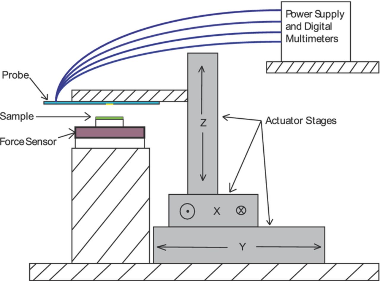
Figure 5. Schematic of measurement stage and probe setup. The probe is mounted in an inverted configuration and descends onto the sample, which is mounted on the force sensor.
While the probe is moved by the actuator stages, the material sample, which is smaller than the probe, is immobilized below it. In the case of battery electrode samples, the current collector of the 2 cm × 2 cm sample was attached to a larger strip of copper foil (for electrical contact), then onto a 3-mm-thick sheet of 20-durometer silicone, then onto the force sensor (Fig. 5). The silicone sheet allows an even pressure to be applied and takes advantage of the conformal properties of the thin-film electrode. The force sensor is an MLP-100 load cell (Transducer Techniques, CA, USA) connected to an NI 9237 4-Ch module in a cDAQ-9171 CompactDAQ unit (National Instruments, TX, USA). This allows pressure to be measured, and by a feedback loop with the Z-position stage, controlled at a desired set point. A PS280 DC power supply (Tektronix, OR, USA) was used to provide a constant voltage to the sample during each test. Four Agilent 34410A Digital Multimeters (Keysight Technologies, CA, USA) monitored the current and voltages. A National Instruments USB-6008 unit was used to provide control signals to relays to change the electrical configuration of the measurements as shown in Fig. 4. The entire apparatus was computer controlled through a LabView (National Instruments, TX, USA) graphical interface.
To ensure consistency of electrode measurements while automating data collection, considerations were given to avoid undue Joule heating or viscoelastic deformation. The voltage applied across the probe (to ground) was kept between 100 mV and 1 V, which kept the current through the electrode under 1 mA. The vertical pressure applied to the battery samples was 150 − 175 kPa, and a rest time of 40 − 120 sec between measurements was implemented to allow for mechanical relaxation as well as dissipation of heat. It was found that repeated measurements at the same location yielded consistent results, showing no accumulation of heat or strain.
Validation of Experimental Design
To validate the micro-four-line probe measurements and inversion technique, electrical tests were performed on two samples: a carbon-black-impregnated silicone sheet (Cho-seal S6600, Parker Chomerics, Woburn, MA) having an average thickness of 863 μm. This material is reported by the manufacturer to have an approximate conductivity of 200 mS/cm, which is within the range typical of Li-ion battery electrodes. Because the material is not attached to a current collector and is relatively thick, a greater range of experiments can be used to test its conductive and contact properties. Secondly, tests were performed on a delaminated Toda HE5050 electrode film.
Electronic conductivity
The electronic conductivity of a 2-cm square piece of the conductive silicone was measured using the μ4LP in the tangential electrical configuration. Sixteen locations near the center were measured, with 5 repetitions at each location. Between each measurement the probe was lifted off the sample for 120 s. The mathematical model was modified to reflect the absence of a current collector (equivalent to infinite contact resistance). In this case, a tangential experiment alone is able to determine material conductivity. Table I shows the mean and the confidence interval of the conductivities across all measurements at all locations.
Table I. Validation of μ4LP measurements using alternative methods on conductive silicone and delaminated Toda HE5050 films. Columns indicate bulk electronic conductivities and current collector interfacial contact resistances, each with 95% confidence intervals; n.a. indicates method not applicable.
| Sample | Method | σ (mS/cm) | R''c (Ω cm2) |
|---|---|---|---|
| c. silicone | μ4LP | 273.7 ± 3.7 | 0.146 ± 0.008 |
| c. silicone | van der Pauw | 265.4 ± 1.5 | n.a. |
| c. silicone | 4PP | 296 ± 15 | n.a. |
| c. silicone | sandwich | n.a. | 0.134 ± 0.028 |
| Toda HE5050 | μ4LP | 9.3 ± 3.7 | n.a. |
| Toda HE5050 | 4PP | 10.0 ± 0.5 | n.a. |
There are two main sources of uncertainties in this work: that for the measurement method itself and that for inherent spatial variation in the sample. Based on the 5 repetitions at each location a standard deviation can be determined, which can be attributed to measurement random error. The average of these standard deviations is 3.0 mS/cm. On the other hand, the standard deviation of the average conductivities for the 16 locations is 16.2 mS/cm, which is indicative of the spatial variability. This means two things: first that the uncertainty in the measurement method is generally less than the inherent spatial variation in the sample, and second that the sample heterogeneity is significant.
Next, the van der Pauw method for measuring resistivity14 was used to benchmark these values. The same piece of silicone was tested, and the average bulk conductivity was recorded (Table I) for 5 distinct measurements, made by permuting the 4 connections to the film. The van der Pauw and μ4LP methods yielded average conductivities within 3% of each other, though their confidence intervals do not overlap. We note that external pressure was not used for the van der Pauw experiment, whereas during the μ4LP measurement the sample was under 75 kPa pressure. It is also worth noting that the van der Pauw method averaged conductivity over a larger and different volume of the sample than did the μ4LP method.
Later in the course of this work, it was determined that additional validation should be done. As shown in Table I, a standard 4-point probe (1.27 mm probe spacing) was used to test 16 locations on a sample of the conductive silicone. The results had higher uncertainty than did the van der Pauw and μ4LP methods, but nevertheless substantiate the prior results.
A second validation material was also tested for bulk conductivity. A 2-cm square section of Toda HE5050 electrode (see below for details) was delaminated from its current collector using the technique described in our prior work.9 In particular, the film was adhered to a glass microscope slide with the aluminum layer facing up. Then the aluminum layer was removed with sequential application of gallium metal and of HCl solution. This exposed the porous film attached to the glass, such that it could be tested with both a 4-point probe and a μ4LP at multiple locations. The μ4LP used for this particular experiment differed from others in this work in that it had a 500 μm line length rather than 3 mm. As shown in Table I, the two methods on the delaminated film agreed within experimental uncertainties. Nevertheless, this particular sample yielded a moderately lower average conductivity than did the HE5050 sample reported in Table II. This could be due to the fact that the two samples were from different batches. Alternatively, the delamination procedure could have partially damaged the fragile 26-μm-thick film. While no obvious damage could be discerned, it is possible that microcracks or surface damage could partially reduce the measured conductivity.
Table II. Bulk electronic conductivity and current collector interfacial contact resistance measurements with the μ4LP from four commercial thin-film electrodes. Uncertainties here indicate spatial variability (standard deviation) across a 3 mm × 3 mm sampling area, not uncertainty in the probe measurements, which is much smaller.
| Electrode Sample | σ (mS/cm) | R''c (Ω cm2) | Data Retained |
|---|---|---|---|
| Toda HE5050 | 16.7 ± 2.0 | 0.589 ± 0.095 | 96% |
| Toda 523 | 201 ± 37 | 0.349 ± 0.153 | 97% |
| Anode CPG-A12 | 1243 ± 98 | 0.776 ± 0.091 | 78% |
Contact resistance
A similar process was carried out to validate the contact resistance measurements of the μ4LP. Four circular samples of the conductive silicone were cut 1.6 cm in diameter. Each sample was pressed against copper foil (acting as a current collector), and was measured twice with the μ4LP under 75 kPa of pressure. The average contact resistance was determined from the mathematical model and averaged as shown in Table I (right) along with a 95% confidence interval.
A "sandwich" method was used to validate this contact resistance measurement. The same four samples of conductive silicone were placed one at a time between two pieces of copper foil of the same diameter. Using a four-terminal technique, a current was run between the copper foils, making a 1-dimensional flow path that can be easily analyzed by assuming a series resistance that includes 2 interfacial contacts. The voltage drop across the copper and the silicone was measured while 75 kPa of pressure was applied. The resistivity of each sample was later measured by the van der Pauw method, which allowed us to determine the bulk resistance. Finally, by difference the contact resistance between silicone and copper was then determined. This sandwich method yielded the average contact resistance reported in Table I.
The values for the contact resistance obtained using the μ4LP differ by 8% from those obtained by direct measurement. The confidence interval for the μ4LP method is completely within that for the direct method, showing the two methods are in statistical agreement at the 95% confidence level.
This analysis suggests that the micro-four-line probe can satisfactorily determine both the bulk electronic conductivity of electrode material and the current collector interfacial resistance.
Tests of Li-Ion Electrodes
The Cell Fabrication Facility at Argonne National Laboratory (ANL) graciously provided two types of commercial-quality cathode samples and one type of commercial-quality anode from their library of electrode materials. The cathodes are Toda 523 (ANL A-C005) and Toda HE5050 (ANL A-C006). The anode is ConocoPhillips graphite CPG-A12 (ANL A-A002). These three electrodes were selected for this study because they spanned a large range of bulk conductivity values.
Spatial tangential and orthogonal measurements
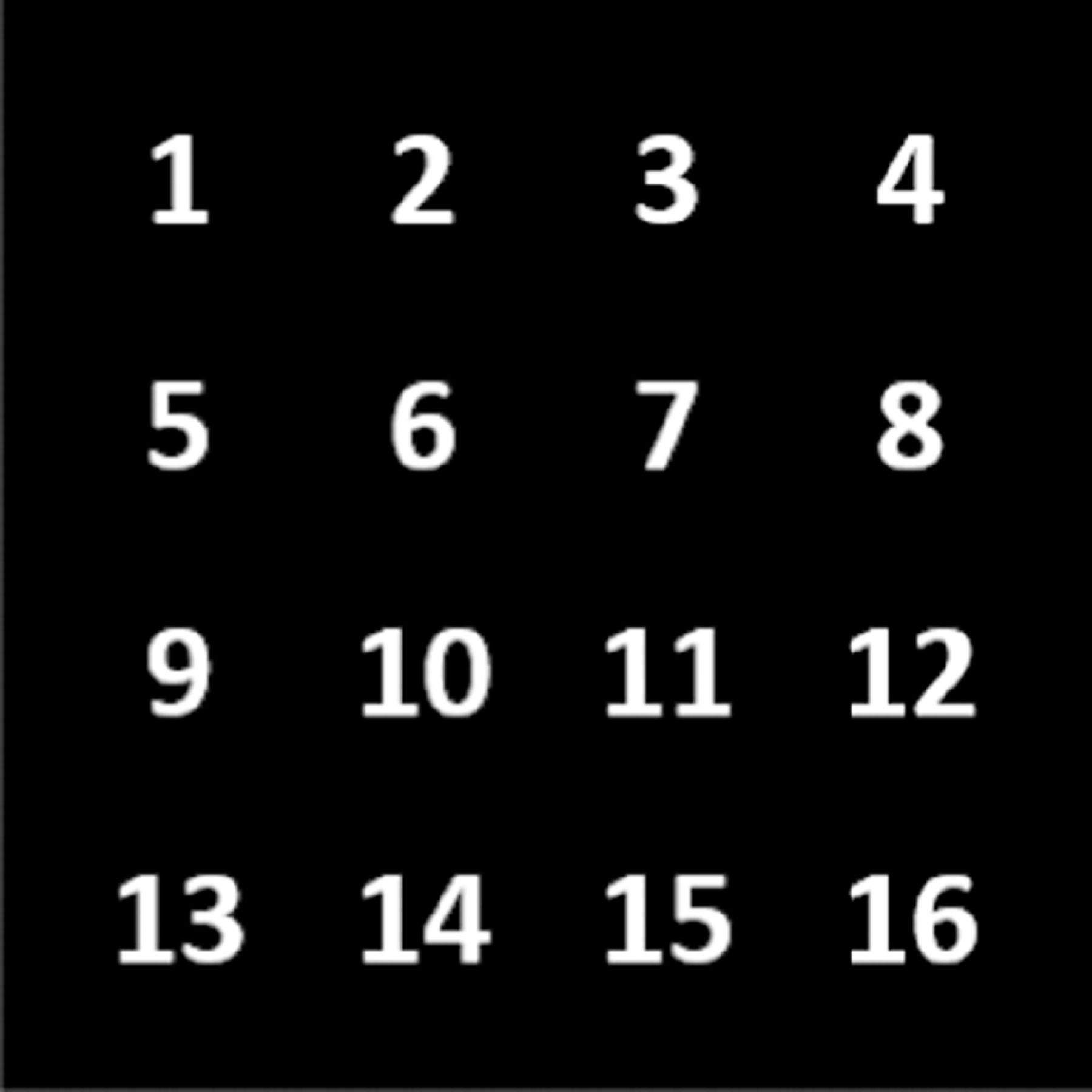
Each dry sample was cut into a 2-cm square and placed onto the test fixture. Measurements were taken by lowering the μ4LP onto the electrode until all four lines made contact with the surface and the desired pressure was reached. The tangential experiment was carried out first. A relay switched the measurement setup (Fig. 4) and the orthogonal experiment was then carried out. The μ4LP was then raised up off of the electrode for 40 s, and the process was repeated for 20 times at one location. The mathematical model processed the measured currents and voltage drops from both experiments, determining the bulk conductivity of the electrode and the contact resistance with the current collector. The electrodes were each sampled at sixteen locations in a grid pattern, with the nearest neighbors 1 mm apart, as shown in Fig. 6.
Statistical check
A statistical check was necessary in order to ensure that the measurements from the μ4LP accurately reflected the true conductivity and contact resistance of the samples. In particular, due to what we attribute to failures of the probe to contact the surface with all four lines consistently, occasional voltage signals that are extremely skewed from a normal distribution would be observed, and so should not become part of the mean value computed for each location. This was particularly noticed for the anode sample, and less noticed for the cathode samples.
To robustly account for such anomalies, a statistical acceptance criterion was used on the data, similar in principle to a median filter. The conductivity and contact resistance for each of the 320 measurements on each electrode were calculated using the inversion procedure. The resulting conductivity points were ordered and a subset composed of the 100 middle points were selected as being most characteristic of the sample. The mean and standard deviation of the subset was calculated. Of the original 320 points, any that were greater than 10 standard deviations from the mean of these 100 points were then rejected from the sample set as being experimental outliers. Then, considering the points that remain after this rejection procedure, the average and 95% confidence interval for the conductivity and contact resistance of each location were computed and reported (see Figs. 7–9). In addition, the percentage of accepted points for the samples is reported (see Table II).
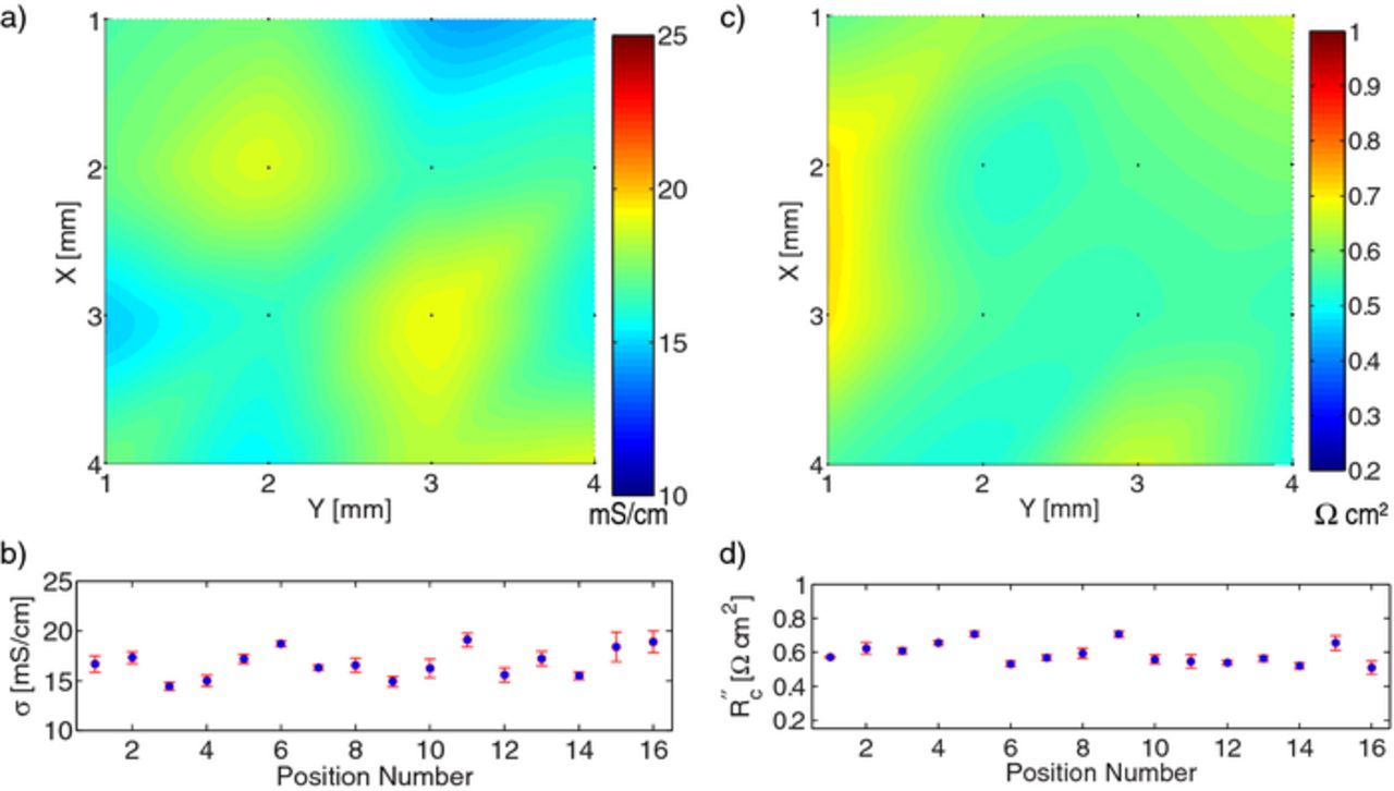
Figure 7. Local conductivity and contact resistance measurements of cathode Toda HE5050 at 16 different locations: (a) spatial map of bulk conductivity, (b) conductivity at each point with 95% confidence interval, (c) spatial map of contact resistance, (d) contact resistance at each point with 95% confidence interval.
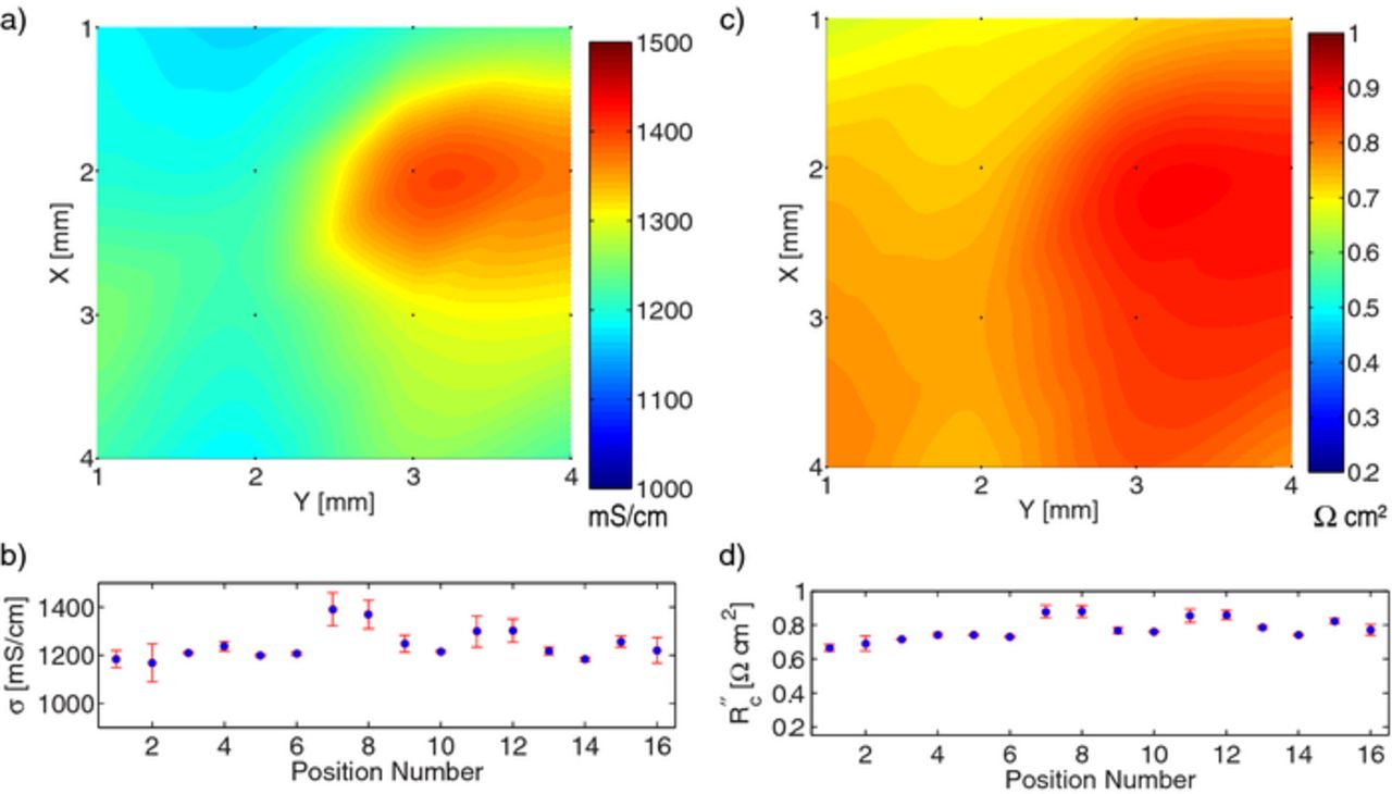
Figure 9. Local conductivity and contact resistance measurements of anode CPG-A12 at 16 different locations: (a) spatial map of bulk conductivity, (b) conductivity at each point with 95% confidence interval, (c) spatial map of contact resistance, (d) contact resistance at each point with 95% confidence interval.
Measurement results
Measurements were performed with the apparatus and procedure described in section Validation of Experimental Design. Contour plots were generated in MATLAB to visualize the data graphically. For each sample film, the computed conductivity and contact resistance as a function of location are plotted: Fig. 7 for cathode Toda HE5050 (A-C006), Fig. 8 for cathode Toda NCM 523 (A-C005), and Fig. 9 for anode CPG-A12.
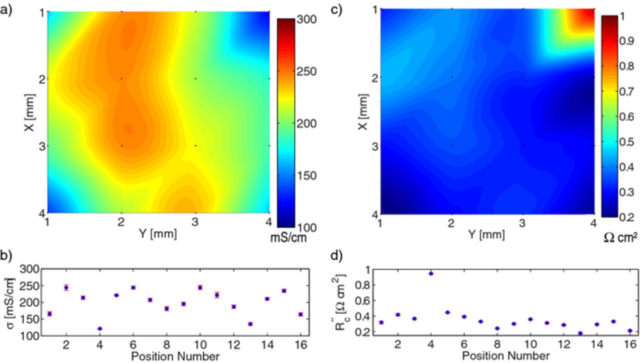
Figure 8. Local conductivity and contact resistance measurements of cathode Toda NCM 523 at 16 different locations: (a) spatial map of bulk conductivity, (b) conductivity at each point with 95% confidence interval, (c) spatial map of contact resistance, (d) contact resistance at each point with 95% confidence interval.
After data for the 16 locations were collected and analyzed, average parameters and spatial variability were determined for each film. These results are shown in Table II. Please note that the ± values in the table are different than those given previously in this work; in this case the standard deviation of the 16 locations is given. As shown in the last column, only a small fraction of the data were rejected in the statistical test.
Discussion
The micro-four-line-probe is able to measure location variability in the electronic conductivity of electrodes. By sampling the conductivity values over multiple locations, a reliable average bulk conductivity of the electrode samples can also be estimated. As seen in Table II, measurements are performed over two orders of magnitude in bulk conductivity. Not surprisingly, the graphite anode has the highest electronic conductivity. The Toda 523 cathode exhibits an average conductivity that is close to our prior measurements on films made from LiCoO2 active material that were delaminated from the current collector.9
It is clear from parts (b) and (d) of Figs. 7–9 that the uncertainty of the μ4LP measurements is, in general, less than the variation from one location to another on the electrode. This implies that a seemingly anomalous conductivity such as at position 4 in Fig. 8 must be due to a material difference at that location because the repeated (descend and lift off) measurements at that location are consistent and do not exhibit greater-than-normal variation. This further suggests that the heterogeneity in electronic conductivity of these two commercial cathodes and commercial anode is significant, even on the millimeter scale.
Another important observation is that even though the bulk conductivity of the electrodes differs by orders of magnitude, the contact resistance of the electrodes is on the same order of magnitude for each of these electrode materials, namely around 0.5 Ω cm2. As electrode specific currents can be on the order of 1 mA cm− 2, average potential drop due to the current collector interface is around 0.5 mV for these electrodes, which is acceptably small.
One might expect the contact resistance to be inversely proportional to conductivity. For instance, a localized concentration of carbon additive or decrease in porosity would both increase σ and decrease R''c. This effect can be mildly observed in Fig. 7 and at position 4 in Fig. 8. However, the opposite trend is observed in Fig. 9. Thus, this expectation is not generally confirmed, suggesting that contact resistance is not easily predicted from film conductivity. Additional measurements in different material systems are planned, to investigate this observation further and determine its general applicability across different material systems.
Conclusions
A micro-four-line probe has been designed, fabricated, and tested, and overcomes many of the challenges inherent in previous conductive property measurements. Thin-film electrodes can be measured without the removal of the current collector, making nondestructive measurements possible. An automated fixture coupled with robust measurement protocols allows accurate, repeatable measurements to be taken with complete pressure control. The ability of the μ4LP when combined with a mathematical model to quantify both the bulk electrode conductivity and the contact resistance has been validated through comparison with standard techniques.
The bulk conductivity and contact resistance of three commercial-quality electrodes were successfully measured and spatially characterized using the μ4LP. These results confirm that there can be significant local variability in the electronic conductivity of pristine commercial-grade Li-ion electrodes.
We anticipate that the methods described here and in the accompanying mathematical paper1 will be of aid to battery manufacturers and researchers to better identify and remedy sources of internal resistance and electrode quality control issues. Electrodes can be tested rapidly and reliably and perhaps, with adaptation of the method, even in real time. Like the samples tested here, most commercial-grade Li-ion electrodes are calendered to flatness and have particles no larger than 15 μm, meaning the current probe geometry is likely to work well. Nevertheless, the geometry of the probe could be adapted as needed for other applications.
The present work suggests several avenues for further exploration. Work is needed to better quantify spatial variability of electrodes at different length scales and for different compositions. Tests could quantify the change in electronic conductivity when electrolyte is introduced into dry electrodes.2,9 Tests could be performed to compare conductivity averages and variations between aged and cycled electrodes and corresponding pristine electrodes. The method could be adapted to measure localized ionic conductivity.15 Additional lines would make the probe more robust mechanically in the case of lost contact with a rough material to be interrogated and would enable additional electrical measurements during a single contact with the sample that improve the estimation capability of the measurement. Moreover, the spatial variability of electrodes could be correlated with microstructural determination and mesoscale models of electrode performance.16–18 Such efforts are planned by our group.
Acknowledgment
This work was partially supported by the Advanced Battery Materials Research (BMR) program of the U.S. Department of Energy. The authors thank Bryant Polzin and Andy Jansen of ANL for providing cell materials.