
Abstract
Cu direct electrodeposition (ED) on a Ta substrate was performed using Pd nanocolloids (NCs) as a Cu nucleation promoter. Pd NCs were synthesized by a polyol method and loaded onto a pretreated Ta substrate. Through a two-step potentiostatic ED process in a pyrophosphate-based electrolyte, a continuous Cu seed layer was deposited on the Ta substrate, although the surface showed irregular morphology. The addition of allyl alcohol improved the surface regularity of the Cu seed layer, allowing the conformal Cu seed layer to be formed successfully on the 55 nm patterned Ta substrate. Cu gap-filling was achieved by galvanostatic ED in a sulfate-based electrolyte on the preformed seed layer.
Export citation and abstract BibTeX RIS
The Cu interconnection process in ultra-large scale integration is composed of the patterning of a low-k dielectric layer, the deposition of a diffusion barrier/Cu seed layer, Cu gap-filling, and chemical mechanical polishing.1–3 Among these steps, the diffusion barrier and Cu seed layer are formed by physical vapor deposition (PVD). Generally, metals deposited by the PVD method show good adhesion with the substrate and superior film properties, such as low resistivity and low surface roughness. However, the problem induced by the poor step coverage of the Cu seed layer has become serious as trenches are being reduced. Various papers have reported the difficulties in Cu gap-filling by ED due to overhang and defects at the sidewalls of the PVD Cu seed layer on narrow trenches.4–7 Therefore, other deposition methods such as chemical vapor deposition (CVD), atomic layer deposition (ALD), electroless deposition (ELD), and direct ED are considered as alternatives to PVD for the formation of the seed layer. Specifically, direct ED has received much interest due to its various advantages, such as its low process cost, short process time, and excellent control of the thickness of the deposited metal.8
Direct Cu ED is defined as the ED of Cu without a Cu seed layer on a heterogeneous substrate such as Ta, Ti, Ir, or Ru. Some papers reported Cu superfilling of sub-micron features as well as seed layer deposition performed by direct ED.4,9–13 Our previous paper described the direct Cu ED on a TiN/Ti diffusion barrier with the aid of a Pd particle which was formed via a displacement reaction.4 The displaced Pd particle assisted in the formation of a uniform Cu film by reducing the charge transfer resistance during the ED process. Thus, defectless superfilling was realized on a 400 nm feature. In addition, studies of direct Cu ED on a Ta-based barrier layer were also published by Kim et al. and Starosvetsky et al. Kim et al. focused on the observation of the growth of Cu films on a TaN substrate after the anodic removal of Ta oxides in a saturated KOH solution.12 Starosvetsky et al. succeeded in the seedless gap-filling of a 300 nm trench which consisted of a TaN/Ta barrier layer after a cathodic pretreatment in a pyrophosphate-based electrolyte.13
Although various approaches have been reported by various research groups, it is still challenging by means of direct ED to fill sub-100 nm trenches covered with highly resistive barriers owing to their low conductivity and large charge transfer resistance. The aforementioned studies applied various strategies, such as native oxide removal or the use of Pd activation; however, the remaining oxides or large Pd particles especially with a wide distribution prohibited the formation of an ultrathin layer and the sub-100 nm feature filling.
Therefore, a feasible direct Cu ED on Ta barrier was investigated in this study in an effort to realize sub-100 nm gap-filling. We introduced well-defined Pd NCs on a Ta substrate to promote the nucleation of Cu on a highly resistive substrate. Pd NCs nearly 3 nm in size and the addition of allyl alcohol in the ED bath facilitated the preparation of a uniform Cu seed layer on a blanket Ta substrate. The seed layer formation method was also successfully applied to a 55 nm patterned Ta substrate. After the deposition of the seed layer, gap-filling of the trenches was accomplished.
Experimental
Pd NCs were synthesized using a microwave-assisted polyol method.14–16 A solution containing 0.003 M K2PdCl6, 0.01 M polyvinylpyrrolidone (PVP, Mw = 40,000 g mol−1), 0.001 M cetyltrimethylammonium bromide (CTAB), and 10 M ethylene glycol (EG) was prepared for the Pd NCs synthesis. The solution was heated in a microwave for 80 s to induce the reduction of Pd ions. After the formation of Pd NCs, centrifugation was used to separate the Pd NCs from the solution. The separated Pd NCs were washed by n-hexane and ethyl alcohol to remove the residual PVP and EG, and then dispersed in ethyl alcohol to make the 0.18 wt% Pd NCs dispersion. The zeta-potential of the synthesized Pd NCs was measured to −53 (±1.9) mV, and this attributed to the excellent dispersing property of the Pd NCs in ethyl alcohol.
Figure 1 illustrates a schematic diagram of the direct Cu ED assisted by the Pd NCs. A blanket or 55 nm patterned SiO2/Si substrate covered with a Ta barrier layer (7 nm, PVD) was used as the substrate. The substrate was cut to 1.5 × 1.5 cm2, and the native Ta oxide was removed by immersing the specimen in a solution containing 1 vol% HF and 1.4 vol% HNO3 for 10 min (blanket) or 3 min (pattern).17 This process not only removes the native oxide but also improves the hydrophilicity of the Ta surface. After the Ta oxide removal process and a subsequent rinsing step, the Pd NCs were loaded onto substrate by coating 0.1 mL of the dispersion, and dried for 15 min at 80°C to evaporate the ethyl alcohol. The amount of Pd NCs loaded on the substrate was about 1.8 μg cm−2, which was confirmed by a quartz crystal microbalance. The improved hydrophilicity of Ta surface after pretreatment facilitated the uniform wetting of the Pd NCs dispersion during the coating process.
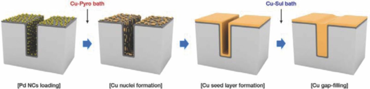
Figure 1. Schematic diagram of the Cu seed layer formation and gap-filling on a patterned substrate with Pd NCs.
The Cu seed layer was formed onto the Pd NC-loaded Ta substrate by direct Cu ED via two steps: a nucleation step and a film formation step. The specimen was loaded to a homemade electrochemical cell which enclosed the substrate exposing only 1 cm2 of the specimen area to the electrolyte. The electrolyte for the deposition of the seed layer consisted of 0.3 M Cu2P2O7 and 1.0 M K4P2O7 (Cu-Pyro bath).13,18 After the deposition of the seed layer, annealing was conducted at 100°C for 30 min in a N2 atmosphere to improve the adhesion of the seed layer.
The electrolyte for the trench filling was comprised of 0.25 M CuSO4 and 1 M H2SO4 (Cu-Sul bath). 88 μM poly(ethylene glycol) (PEG, Mw = 3400 g mol−1), 1 mM NaCl, and 50 μM bis-(3-sulfopropyl)-disulfide (SPS) were added as additives for the trench filling.19–22 Prior to the gap-filling, the Cu native oxide on the Cu seed layer was removed using a 0.02 M citric acid and 0.03 M KOH solution for 30 s.23
A potentiostat (EG&G, PAR 273A) was used for the ED process and the electrochemical analysis with Ag/AgCl as the reference and a Cu rod as the counter electrode. A field emission scanning electron microscope (FESEM; JSM-6700F, JEOL), a transmission electron microscope (TEM; JEM-2100F, JEOL), and an atomic force microscope (AFM; 5100 AFM, Agilent Technologies) were utilized for the microscopic observation. A focused ion beam (FIB; Quanta 3D FEG, FEI) was used to prepare the specimen for the TEM analysis.
Results and Discussion
The synthesized Pd NCs that would act as a promoter for Cu nucleation were analyzed by TEM. The TEM observation was conducted after sampling and drying the Pd NCs dispersion on TEM grid (Formvar Grid 100mesh, Cu). As shown in Figure 2a and 2b, the synthesized Pd NCs had a uniform size distribution with average size of 3.0 (±0.4) nm. The distribution of Pd NCs on Ta substrate after loading was also evaluated by comparing the surface morphology measured by AFM. As can be seen in Figure 2c and 2d, the surface morphology was rarely changed except the slight increase in the surface roughness, indicating that no severe aggregation of Pd NCs occurred on the surface. Therefore, it could be expected that the Pd NCs were quite uniformly distributed over the Ta substrate after loading. Because both the Pd NCs and Ta substrate had negative zeta-potential at the pH range of the experiment, it was supposed that the physical rather than electrostatic force would be the origin of the fixing force between the Pd NCs and Ta substrate.24,25

Figure 2. (a) TEM image of synthesized Pd NCs on TEM grid and (b) number probability of Pd NCs according to the particle size. (c) and (d) illustrate the AFM surface morphology of Ta substrate (c) before and (d) after Pd NCs loading.
After removing the ethyl alcohol by drying, the deposition of the Cu seed layer on the highly resistive Ta barrier was performed using a basic Cu-Pryo bath. Generally, the use of basic electrolyte gives higher nucleation density on highly resistive substrate during the ED, which facilitates the formation of the continuous Cu seed layer.26–28 The Cu seed layer formation step was composed of two potentiostatic ED steps; a nucleation step and a film formation step. The deposition potential and charge amount in each case were fixed to −1.45 V (vs. Ag/AgCl) and 6 mC cm−2, respectively. During the nucleation step, the Cu nuclei were primarily developed on the loaded Pd NCs because the Pd NCs promoted the electron transfer.4 During the film formation step, Cu film formation was completed via the coalescence between the Cu nuclei. Consequently, 18 (±4.8) nm of Cu film was deposited on the Ta substrate, as depicted in Figure 3a. However, the seed layer showed an irregular thickness with a root mean square roughness (Rrms) value of 10.7 nm, as shown in Figure 3c. The non-uniform thickness distribution resulted from the preferential growth of the deposited Cu during the film formation step. Cu nuclei which developed on Pd NCs during the nucleation step would prompt the Cu ion reduction even more than Ta or Pd NCs. Cu film deposition with a rough surface morphology would not be avoidable in the event of non-uniform growth.
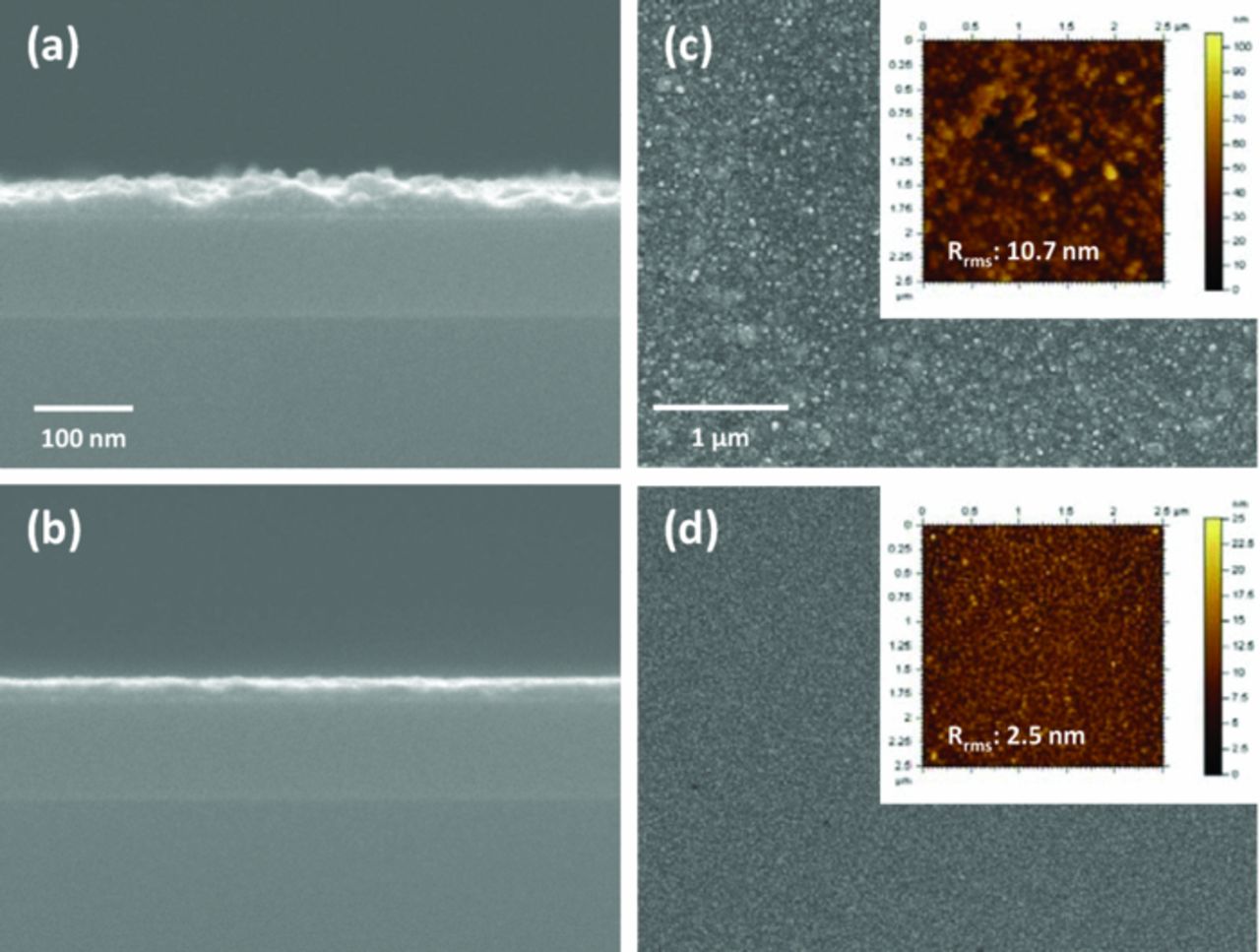
Figure 3. FESEM images of Cu films on Pd NC-loaded Ta substrates deposited (a, c) without allyl alcohol and (b, d) with 0.035 M allyl alcohol. (a, b) depict the cross-sectional and (c, d) describe the surficial FESEM images. Inset in (c, d): AFM image of each film.
In order to solve the surface roughness problem, allyl alcohol, which has been applied as a leveler during the deposition of a Cu-Zn alloy in a pyrophosphate-based electrolyte, was adopted.18 Despite the lack of information, it was reported by Senna et al. that allyl alcohol suppressed the Cu deposition by forming a stable complex with Cu ion, and improved the surface uniformity during the Cu-Zn alloy deposition process. Similarly, in this study, the addition of 0.035 M allyl alcohol into the Cu-Pyro bath also suppressed the deposition process and improved the uniformity of the Cu seed layer, as presented in Figure 3b and 3d. Owing to the brightening effect of the allyl alcohol, the thickness of the Cu seed layer decreased to 12 (±1.2) nm and the Rrms value was reduced to 2.5 nm.
The adhesion of the Cu seed layer was tested via the tape test method following ASTM D 3359.29 As described in the method, the film was divided into 30 (±2) squares by cutting tool and the percent area removed (PAR) value was calculated after the tape test. The adhesion of the Cu seed layer was markedly improved by the thermal treatment at 100°C for 30 min, decreasing PAR value from 19.4% to 6.7%. The improvement also had a positive influence on the subsequent Cu ED. Without the thermal treatment, peeling-off of Cu deposit was observed when a 100 nm-thick Cu film was electrodeposited on the seed layer. On the other hand, the film remained intact on the thermally-treated Cu seed layer showing the PAR value of 12.5%. Therefore, the thermal treatment was performed after the seed layer formation in all cases.
Subsequent to the seed layer formation, linear sweep voltammetry (LSV) in a Cu-Sul bath was conducted on the seed layer. As depicted in Figure 4, the Cu deposit formed on the blanket Ta gave the lowest current density, and the on-set potential for the Cu reduction (ηred, Cu) was −0.4 V (vs. Ag/AgCl). This occurred because the Cu film was not completely formed on the bare Ta substrate. In contrast, ηred, Cu was positively shifted to 0.1 V (vs. Ag/AgCl) on the Cu seed layers deposited on the Pd NC-loaded Ta substrates. At the same time, the current density was high on the Cu seed layers in all of the potential ranges investigated. Despite the similar ηred, Cu value, a higher current density was observed on the Cu seed layer deposited without allyl alcohol compared to that deposited with 0.035 M allyl alcohol, as expected given that ally alcohol reduced the surface roughness.
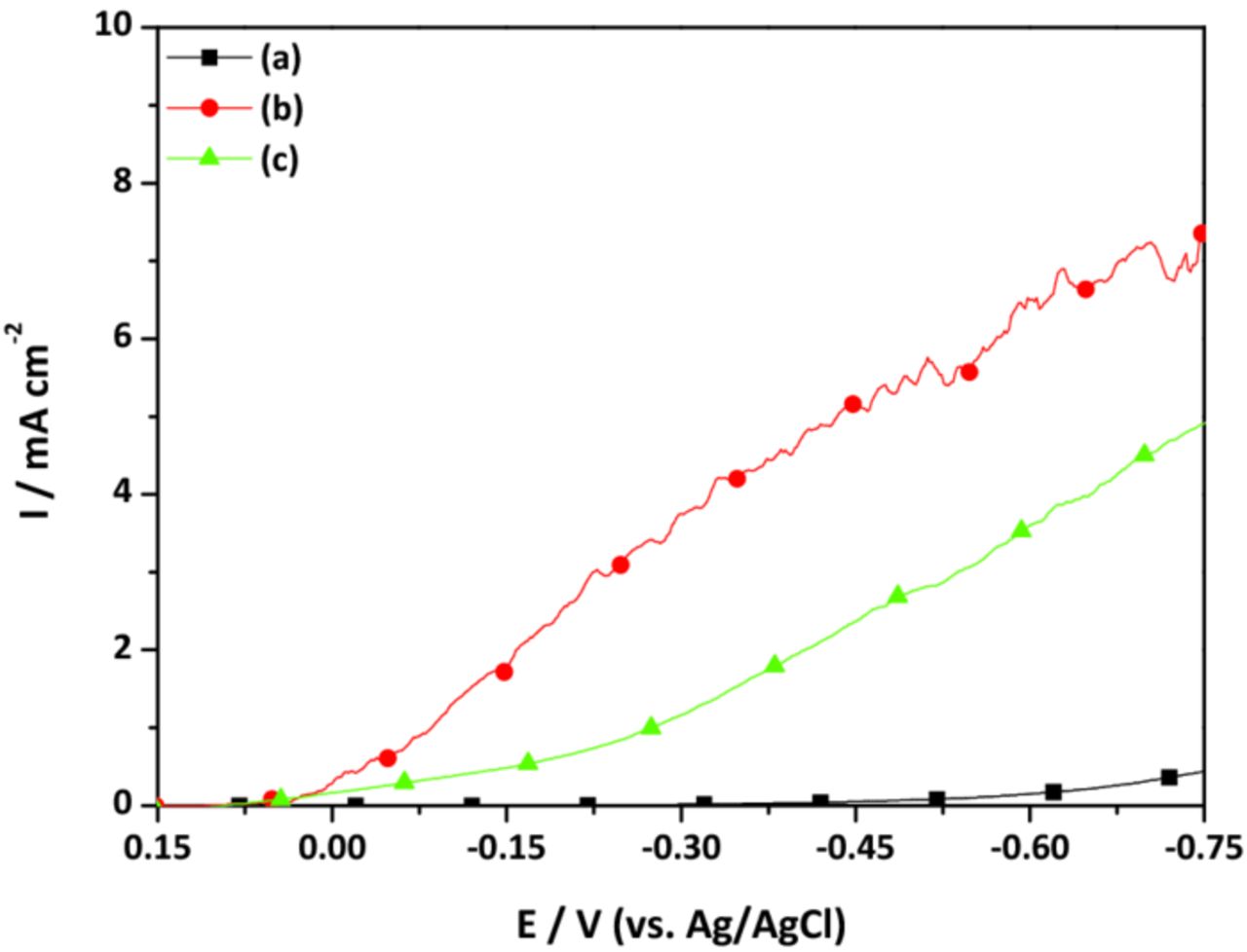
Figure 4. LSV on (a) Cu deposit formed on the blanket Ta, (b) Cu seed layer deposited on the Pd NC-loaded Ta without allyl alcohol, and (c) Cu seed layer deposited on the Pd NC-loaded Ta with 0.035 M allyl alcohol. LSV experiment was conducted in Cu-Sul bath (scan rate = 10 mV s−1).
The effect of the additives, an accelerator and a suppressor, all of which are essential for trench filling in a Cu-Sul bath, was also tested on a Cu seed layer by LSV. A seed layer deposited on the Pd NC-loaded Ta with 0.035 M allyl alcohol was used to test the additive effect. In Figure 5, the additives worked well on the seed layer, as on a conventional Cu electrode.20–22 That is, a combination of PEG and Cl− suppressed the reduction of the Cu ions, and the addition of the SPS accelerated the Cu ion reduction on the seed layer, as usual.

Figure 5. LSV on Ta substrate covered with Cu seed layer prepared in Cu-Pyro bath containing 0.035 M allyl alcohol (scan rate = 10 mV s−1). The concentration of each additive is specified in the experimental session.
Direct Cu ED was also applied to a 55 nm patterned Ta substrate to form a seed layer and to fill the trench. Figure 6a and 6d present the 55 nm patterned substrate covered with 7 nm of a Ta barrier layer. When Pd NCs were not loaded, only irregular Cu islands were observed on the rib of the trench after the seed layer formation steps (Figure 6b and 6e). In contrast, a Cu seed layer was deposited on the bottom, side, and top of the trench of the Pd NC-loaded Ta substrate, as depicted in Figure 6c and 6f, although the uniformity of the seed layer was poor, as expected. Therefore, allyl alcohol was also used during the seed layer formation process on the trench.
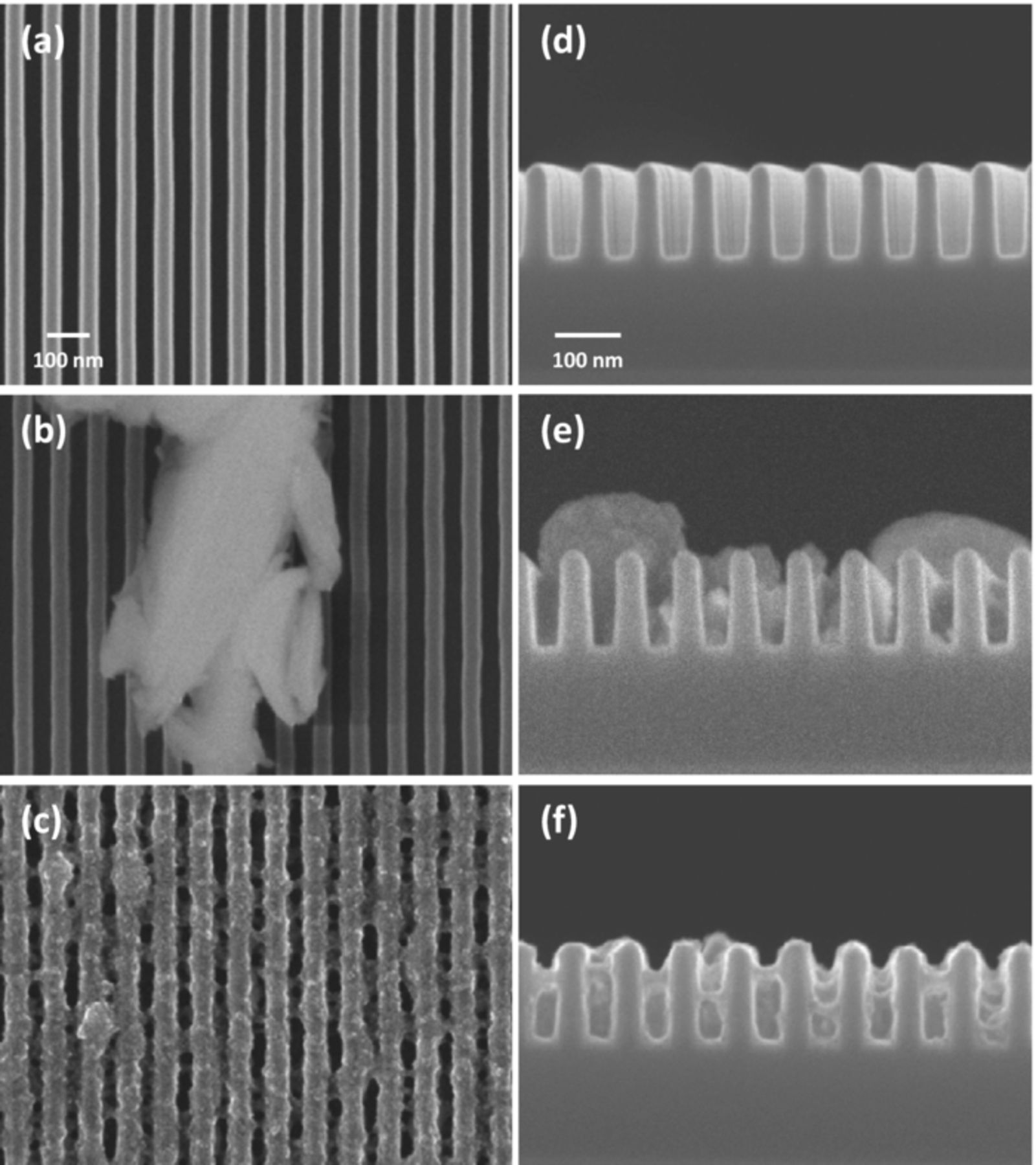
Figure 6. FESEM images of 55 nm patterned Ta substrate (a, d) before seed layer deposition and after seed layer formation (b, e) without Pd NCs and (c, f) with Pd NCs.
The effect of the allyl alcohol content on the uniformity of the seed layer was investigated by FESEM images, as depicted in Figure 7. These images show that the uniformity of the seed layer was gradually improved with increase in the concentration of allyl alcohol. To compare the seed layer uniformity quantitatively, the trench opening after the formation of the seed layer was measured, as shown in Figure 8a. Finally, when 0.07 M of allyl alcohol was added, the width of the trench opening approached to that of a Ta substrate, which was sufficient to be applied for the trench filling step. Based on the TEM image in Figure 8b, the thickness of the seed layer was measured as 5.1 (±0.3, bottom) nm, 4.3 (±0.3, side) nm, and 5.5 (±0.6, top) nm, indicating the formation of a conformal seed layer.
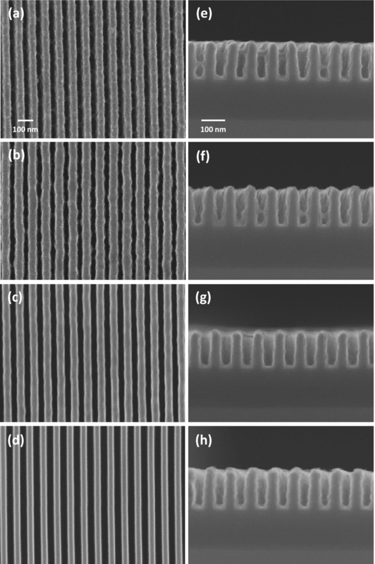
Figure 7. FESEM images of seed layer deposited on 55 nm patterned Ta according to the allyl alcohol concentration. Allyl alcohol content in Cu-pyro bath was (a, e) 0.0175 M, (b, f) 0.035 M, (c, g) 0.0525 M, and (d, h) 0.07 M.
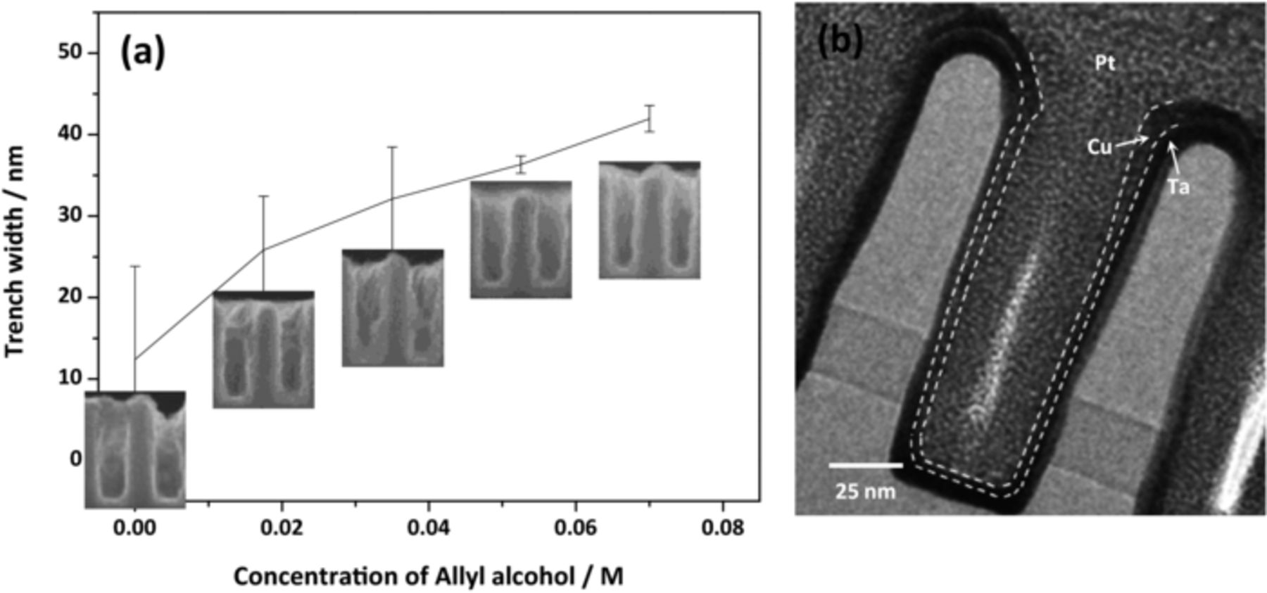
Figure 8. (a) Trench opening width after Cu seed layer formation with varying the allyl alcohol concentration in Cu-Pyro bath and (b) the TEM image for the Cu seed layer deposited with 0.07 M allyl alcohol (Pt was sputtered before the TEM specimen preparation by FIB).
The brightening effect was not observed on the patterned substrate with 0.035 M allyl alcohol, which was sufficient concentration on the blanket substrate. It indicated that the surface concentration of allyl alcohol would change with the surface area of the substrate at the same bulk concentration. Therefore, the increased allyl alcohol concentration (0.07 M) was required for obtaining the smooth deposit on the patterned substrate, due to the large surface area of the patterned substrate compared to that of the blanket substrate.
Galvanostatic ED was carried out to fill the trench covered with the seed layer. A Cu-Sul bath was used in combination with PEG-Cl−-SPS as additives for the filling. The applied current was set to 5 mA cm−2 and the deposition process was stopped when the accumulated charge amount exceeded 300 mC cm−2. TEM observation result after cutting by a FIB is illustrated in Figure 9. Without any defects or voids, a 55 nm patterned substrate was successfully filled.
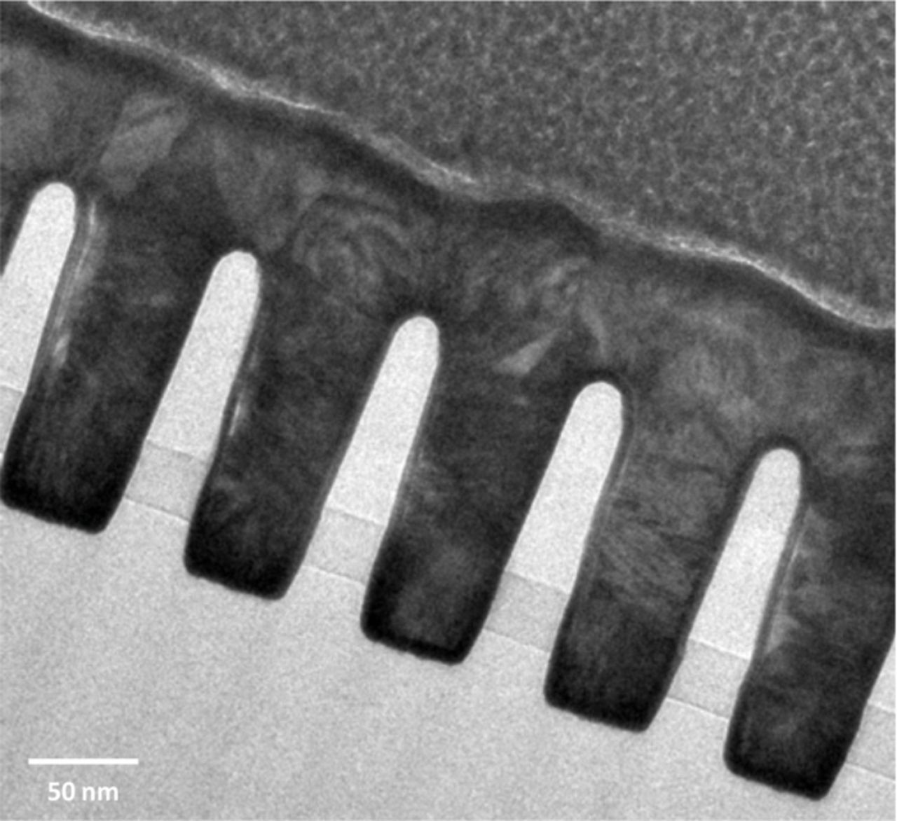
Figure 9. TEM analysis of 55 nm patterned trench covered with the seed layer after filling in Cu-Sul bath.
Conclusions
Direct Cu ED on Ta assisted by Pd NCs was conducted to prepare a thin Cu seed layer. With the aid of Pd NCs as a Cu nucleation promoter, a continuous 18 (±4.8) nm Cu seed layer with an Rrms value of 10.7 nm was deposited on a Ta substrate after two-step potentiostatic ED process in a Cu-Pyro bath. The addition of allyl alcohol improved the uniformity of the seed layer with a reduction in the thickness to 12 (±1.2) nm and with a reduced Rrms value of 2.5 nm. Using allyl alcohol, a 5 nm-thick Cu seed layer was also conformally formed on a 55 nm patterned Ta substrate. After the formation of the seed layer, trench filling was also realized via galvanostatic ED in a Cu-Sul bath.
Acknowledgment
This work was supported by the Incheon National University Research grant in 2011.