Abstract
In this paper, we discuss the use of broadband high frequency electromagnetic waves (RF) to non-destructively identify, classify and characterize performance-limiting defects in emerging nanoelectronic devices. As an illustration, the impact of thermal cycling on the RF signal characteristics (insertion loss (S21) and return loss (S11)) is used to infer thermo-mechanical stress-induced defects in metal interconnects. The inferred defects are supported with physical analytical data where possible.
Export citation and abstract BibTeX RIS

This is an open access article distributed under the terms of the Creative Commons Attribution 4.0 License (CC BY, http://creativecommons.org/licenses/by/4.0/), which permits unrestricted reuse of the work in any medium, provided the original work is properly cited.
In this paper, we discuss the use of broadband radio frequency (RF) to non-destructively identify and characterize performance-limiting defects in emerging nanoelectronic devices. To do this, we reinterpret previously published (mostly from reference 1), and some new data, to demonstrate the utility of RF phase data in failure mode analysis, to detect structural changes in devices, without resorting to the traditional destructive physical analysis.
Emerging nanoelectronics are rapidly adapting three dimensional integrated circuits (3D-ICs), enabled by through-silicon vias (TSV), as a strategy to increase performance and functional diversification. However, the introduction of such 3D-ICs to the market has been hindered by reliability challenges such as stress related failures. Specifically, the stress buildup due to mismatch in the coefficient of thermal expansion (CTE) of the materials of construction results in the generation of defects such as cracks, voids, delamination, plastic deformation, substrate warping and buckling.1 These types of damage ultimately lead to open or short circuits in the devices, resulting in catastrophic failure. While metrology for accurate quantification of the impact of stress evolution in interconnect structures is needed, further insights are required to characterize and understand the physical damage stemming from the stress buildup. Microwave (RF)-based metrology tools offer several advantages over the traditional techniques and are uniquely suitable for studying the buried structures and interfaces inherent in such nanoelectronic devices. For example, changes in RF insertion losses offer early prognostics of the onset of failure in ball grid arrays (BGA) subjected to accelerated temperature cycling tests.2,3 RF measurements have also been used to specifically show that leakage conductance increased with the degree of voiding damage in Al and AlCu metal interconnects lines in integrated circuits.3 As well, such high frequency measurements have been used to monitor TSV interconnect performance.1
When an electromagnetic wave propagating in a transmission line encounters a discontinuity, parts of the wave are either scattered, transmitted or reflected. The resulting signal losses, due to reflection and transmission, can be explained by changes in the resistive, inductive and/or capacitive properties of the line. Detailed study of the transmitted and reflected signal losses, therefore, can provide insights into physical changes in the device under test (DUT), since RF based measurements interrogate the entire device under test. Thus, intuitively, broadband RF interaction with devices potentially affords the diagnostics to enable in-situ deduction of failure modes and mechanisms without the need for physical failure mode analyses (FMA).
Sample and Experiment Description
Samples
Two types of interconnects will be discussed in this paper: the traditional planar AlSiCu-based local interconnects and the emerging TSV global interconnects to enable three-dimensional integration (3D-ICs).
For the planar local interconnects, we used a dedicated multi-metal level test structure, manufactured with the TSMC 0.35 μm process flow. The four metal levels, denoted as M1 (deepest) to M4 (closest to chip-air interface), respectively, are as depicted schematically in Figure 1.c In this representation, the top metal lines arrays (M4 and M3) are exposed to air, the middle metal line array (M2) is located about 800 nm beneath the bulk surface, while the bottom metal line array (M1) are located about 2000 nm below the dielectric surface (about 1000 nm below the M2) respectively.
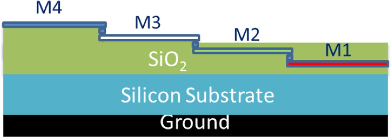
Figure 1. Schematic Plan view of 4-level BEOL test structure: M3 and M4 are exposed, while M2 and M1 lines are encapsulated in SiO2.
For studying prototypical 3D-global interconnects, a two-level stacked-die mechanical test vehicle provided by SEMATECH (Albany, NY) was used. The TSVs were nominally 5.5 μm in diameter and 50 μm deep and were located in the top chip. The TSVs are isolated from the bulk silicon substrate by an isolation liner comprised of an insulating dielectric layer (0.5 μm thick SiO2), barrier layer (0.025 μm thick TaN) respectively. The bottom and top chip wafers were bonded together with benzocyclobutene (BCB). Figure 2(a), shows the layout of the ground-signal-ground (GSG) configured test structure used in this work. Figure 2(b) shows its cross-sectional scanning electron microscopy (SEM) image. The components of the two bonded wafer stack are clearly delineated in later figure. During the RF measurement, a ground-signal-ground (GSG) test probe was placed on the GSG bond pads at both ends of the test structure. For the proof of principle RF reliability study, thirty-four samples, chosen randomly across a single 300 mm wafer, were used.
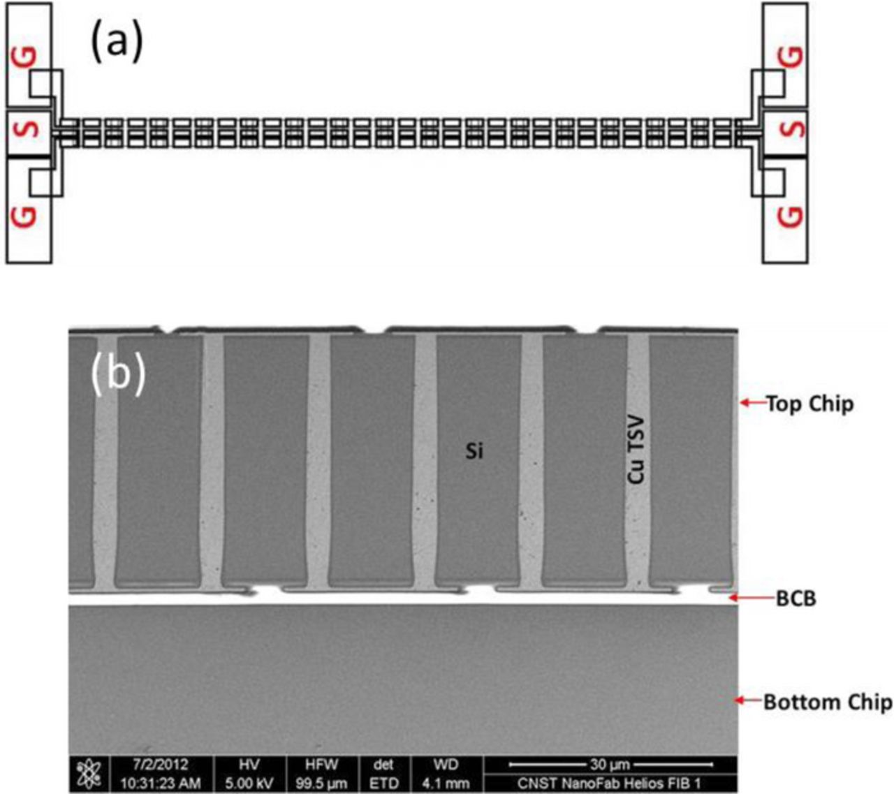
Figure 2. Image of the two-level stacked die test structure (a) Layout of the structure, having a GSG configuration (b) SEM cross-sectional image of the stacked chip.
Experimental
Thermal cycling was used to perturb and induce defects in the devices studied as described elsewhere.1 In brief, the samples were heated from 30°C to 150°C and then cooled to 30°C in laboratory ambient or under a nitrogen blanket. The insertion loss measurements, described elsewhere,1 were first measured on the devices under test (DUT) in the "as-received" state, prior to thermal cycling, to determine their baseline RF signal characteristics. The DUTs were re-measured every 500 thermal cycles, for up to a maximum of 2000 thermal cycles, on a PNA N5230A (Agilent, Santa Clara, CA).c, 1
Scanning Microwave Microscopy (SMM) was used in studying the reflectance loss (S11) of the planar AlSiCu-based interconnect.4 The SMM implementation as discussed here, applies a high frequency signal through a 50 ohm transmission line terminated with a scanning probe microscope tip to the sample.4,5 The SMM generates spatially localized images from the reflected RF (S11) signal amplitude and phase, usually at resonance (around 7 GHz for the set-up used in these studies). The signal from the tip, depending on the skin depth, can reach relatively deep (on the order of tens of microns) into sample and interacts with the buried structures and interfaces. This interaction translates into the changes of the measured reflection coefficient S11. As discussed below, we have demonstrated the subsurface imaging capabilities of SMM on buried integrated circuit metallization. To distinguish from 2-port RF scattering data presented later, scattering parameter data from the SMM method will be denoted as S11SMM.
Results and Discussion
During fabrication, and in-service usage, microelectronic devices are subjected to constant fluctuations in temperature. Such thermal cycling results in the buildup of stress in the TSVs.6 This occurs due to their confinement and the mismatch in the coefficient of thermal expansion (CTE) of Cu (16.7 ppm/°C), with respect to the surrounding Si matrix (2.3 ppm /°C), thus leading to the formation and growth of defects such as voids, and possible delamination at interfaces.7 The defects act as RF signal "scattering centers" resulting in the increase in the insertion loss. Thus, proper interpretation of the RF signal loss traces could help pinpoint or classify defect types. In this section, we demonstrate the inherent in-situ FMA capabilities of the RF-sample interaction by identifying and classifying the defect types suggested from the interpretation of the signal loss traces. Where possible, we support the defect classification with the results of physical analyses based on focused ion beam (FIB) based scanning electron microscopy (SEM) images.
Figure 3 compares the S11SMM amplitude and optical micrographs of the planar local interconnects (described in Figure 1) samples "as-received" ("a" and "c") to the same area after 1000 thermal cycles ("b" and "d"). The reflective losses were evaluated at 7 GHz on the scanning microwave microscope. For the M3 line arrays, the data show increased reflective signals (relative to the glass dielectric background) on the exposed metal lines after 1000 cycles as shown in the lower box of Figures 3a and 3b. The AFM topographical data, collected simultaneously with the S11SMM data, also showed enhanced roughness on the exposed M3 after the 1000 thermal cycles. Furthermore, detailed inspections of the optical micrographs, i.e., comparisons of Figures 3c and 3d, revealed extensive corrosion of the exposed M3 metal line array after the thermal cycling, when compared to the unexposed and insulated M2 line array. Thus, we attribute the increased reflective RF, and increased roughness to the presence of dielectric corrosion byproducts on the M3 after thermal cycling. The corrosion of the metal lines is possibly due to traces of oxygen and water vapor in the nitrogen ambient used during the thermal cycling.8
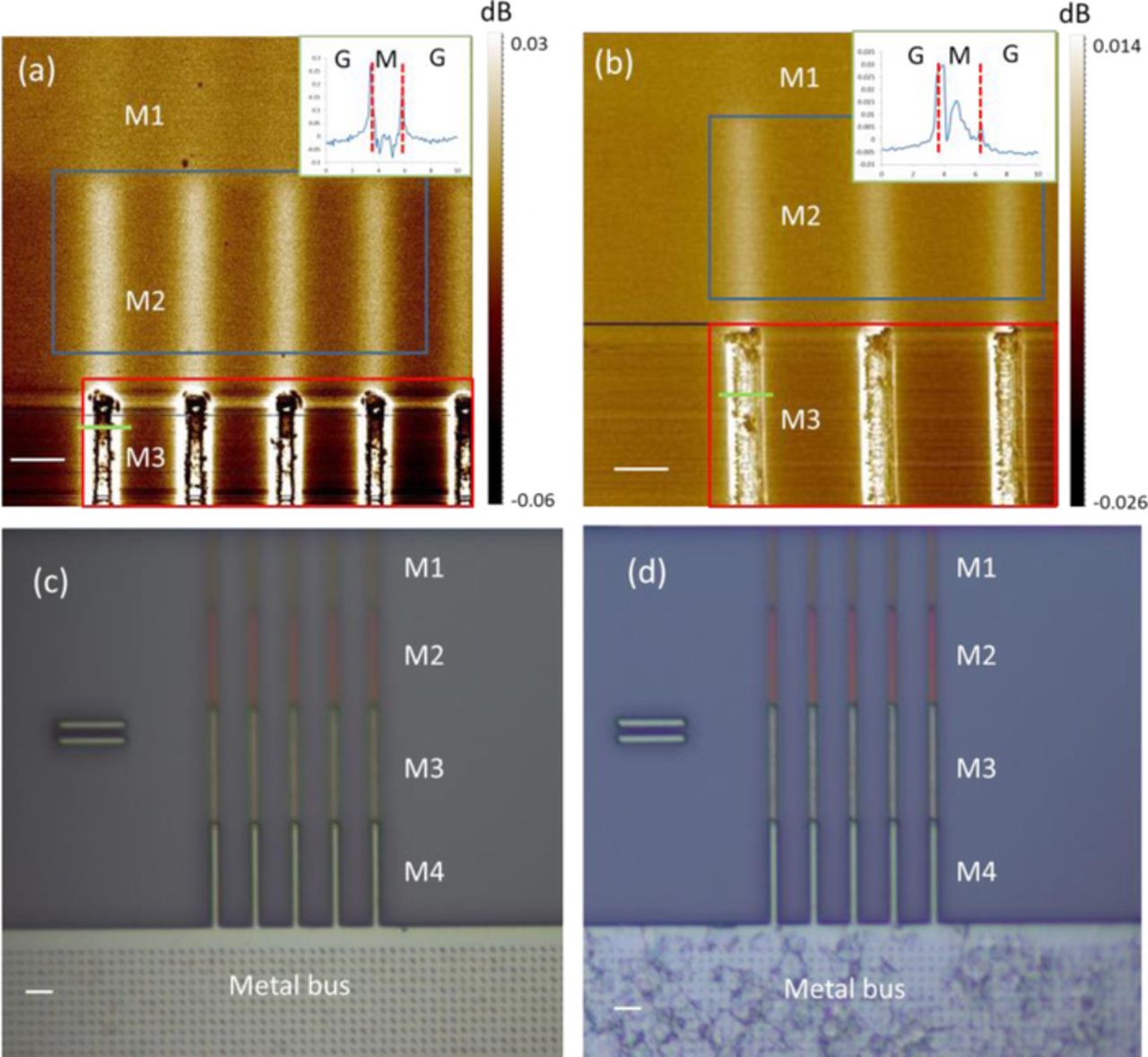
Figure 3. (a) S11SMM amplitude map of 'as-received" (b) S11SMM amplitude map of representative features after 1000 thermal cycles at 7 GHz. Insets are line profiles across single M3 traces, to show the relative RF reflectance off the metal and the surrounding dielectric (from the S11SMM maps, ."M" denotes metal while "G" stands for glass). (c) and (d) are optical images before and after 1000 thermal cycles, respectively. The white scale bars in each image represents 5 μm.
Transmission data is also obtained based on a two-port measurement on a PNA. The through-reflect-line (TRL) calibration method is used to remove cables and connectors in order to establish the reference plane at the tip of the GSG probes. In this study, transmission behavior was used to quantify the changes occurring in the various structures based on loss (amplitude) and phase changes in the transmission performance. The combination of loss and phase change can provide information on the changes associated with resistance and inductance associated with the metal and capacitance associated with the dielectric in the DUTs before and after thermal stresses are applied to the DUTs.
Figure 4 shows the insertion losses (S21) magnitude, in the 0.7 GHz to 40 GHz frequency range, as a function of the number of thermal cycles for the prototypical TSV samples.d Similar to the S11 data for the planar samples, the S21 losses increased with increasing number of thermal cycles. Notice that the S21 magnitude profile of the device under test after thermal cycling is much different from the 'as-received' sample. For instance at 40 GHz, after 2000 thermal cycles the TSV chain's insertion loss degraded by a factor of about 2.4 from its unstressed state (as-received). Furthermore, the degree of deviations of the subsequent traces from the 'as-received trace' shows a strong RF frequency dependence. Specifically, the deviations at frequencies below 5 GHz are much smaller than at higher frequencies, with a very significant roll-off above 25 GHz. Additionally, the RF trace signature is observed to change most drastically after 1000 cycles. The deterioration in the RF characteristics of the TSV interconnect is a clear indication of the damage that have occurred in the structure, such as voids, cracks, delamination and much more, with thermal cycling. The drastic change in the insertion loss profile after 1000 cycles suggests the onset of additional or the exacerbation of existing reliability problems within the DUT.
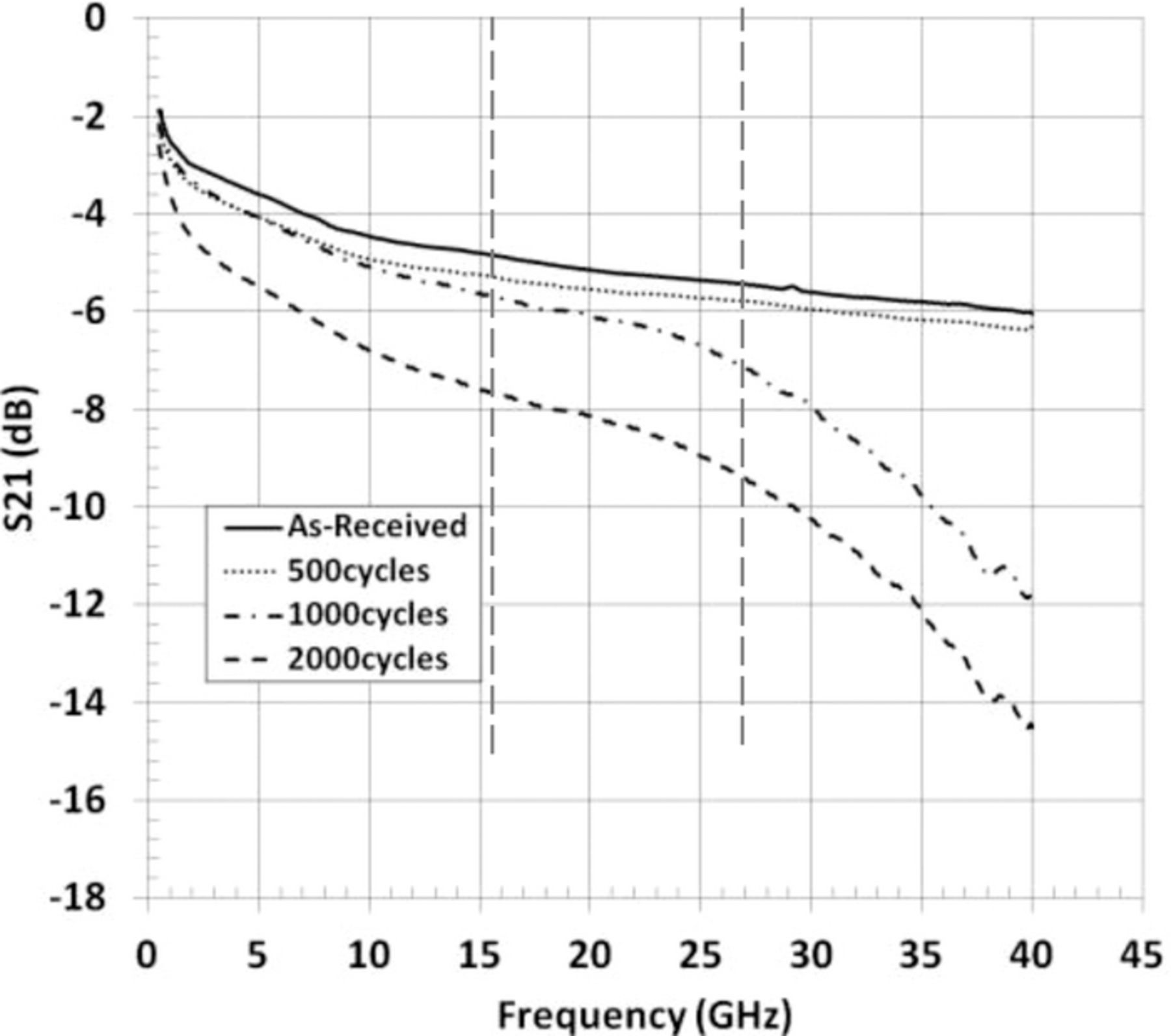
Figure 4. Effect of the number of thermal cycles on the magnitude of the transmission coefficient (S21) as a function of frequency for a single test sample.
The frequency dependence of the S21 signal deterioration suggests that the broadband RF probes different regions of the DUT, in a manner determined by the 'skin effects'. The penetration depth of the incident electromagnetic waves at the operating frequencies can be calculated using equation 1, where δ is the skin depth, ρ is resistivity of the conductor; ω is angular frequency of current = 2πf and μ is absolute magnetic permeability of the conductor.
![Equation ([1])](https://content.cld.iop.org/journals/2162-8777/4/1/N3113/revision1/jss_4_1_N3113eqn1.jpg)
As discussed above, we can distinguish between main types of failures, those responsible for signal losses at below 10 GHz and those above 20 GHz. For interconnects, such as TSVs, the RF-induced current at high frequencies (greater than 10 GHz), is concentrated at the metal-dielectric interface; i.e., the interface between the Cu and the surrounding barrier (Ta/TaN) and isolation liners (SiO2) due to the skin depth phenomenon. Thus, a higher frequency electromagnetic wave penetrates less into a TSV, than a low frequency wave.
Figure 5 compares the cross-sectional FIB-SEM images of sections of Cu filled TSV of "as-received" sample to that after 1000 thermal cycles, to show the impact of the thermal cycling on the materials of construction. The losses below 20 GHz suggest that there may be pre-existing small defects in the body of the Cu-fill (as shown in Figure 5a). After 1000 cycles, these defects grow and coalesce, as shown in Figure 5b, and significant S21 deviation and roll off. Defect types such as cracks and delamination can occur at the bulk Cu-fill–isolation layer interface, and contribute significantly to the S21 signal loss above 20 GHz.
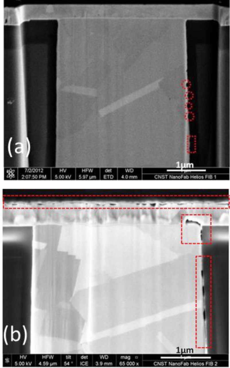
Figure 5. Defects within the Cu filling of the TSV. (a) As-received (b) After 1000 cycles.
Changes in signal propagation characteristics (e.g., S11 amplitude and phase) of device under test are related to the changes in the characteristic impedance of the device.2 In analogy to a microstrip transmission line, the dielectric constant of the medium surrounding the signal carrying lines determines the phase velocity of the electromagnetic waves through the devices under test.9 Figure 6 shows the evolution of the signal phase (phase velocities) in the Cu filled TSVs, as a function of the number of thermal cycles endured, in the prototypical 3D-ICs studied. Below 500 cycles, the phase constants are similar and linear up to 40 GHz. Above 1000 cycles, the phase constant is different and starts to show linear and non-linear behaviors. At the high thermal cycles, the phase response is linear up to 15 GHz. The slope remains linear, but changes up to 28 GHz; above 28 GHz, it becomes slightly non-linear. These changes are indicative of significant changes in the propagation velocity of electromagnetic within the devices under test (DUTs) with increasing number of thermal cycles.
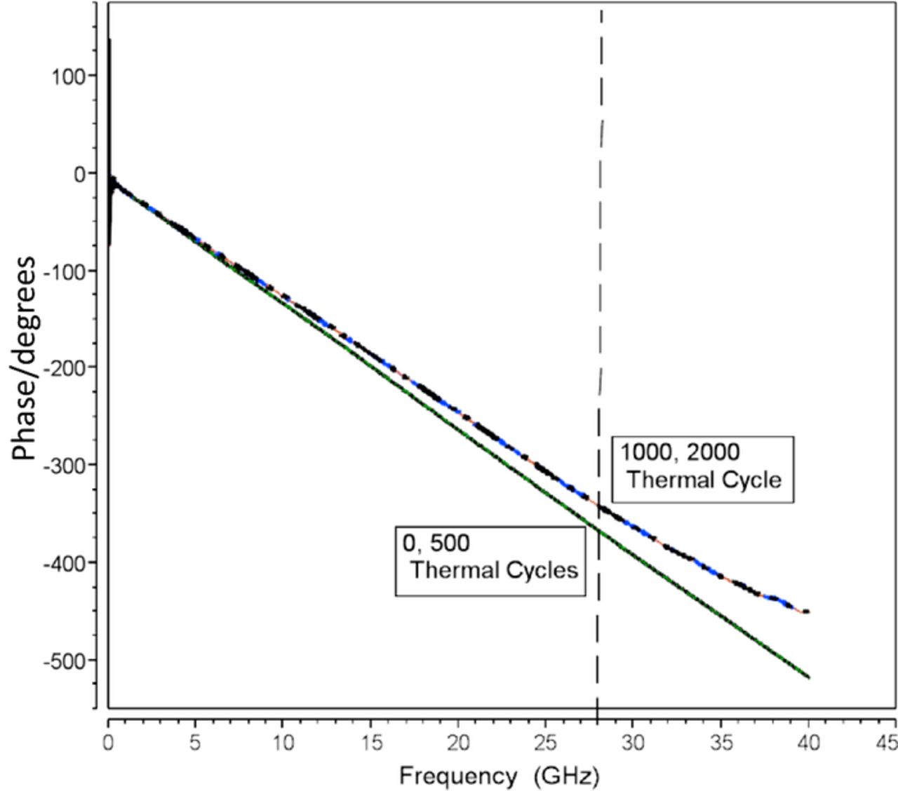
Figure 6. Variation of the Slope of Signal Phase Angle with number of thermal cycles endured by devices under test. The solid trace represents the data for 'as-received' and at 500, while the solid trace represents that data for 1000 and 2000 thermal cycled DUTs respectively. The vertical dashed line at 28 GHz represents the transition from linear to non-liner phase shift for the 1000 and 2000 cycle DUTs.
In Figure 6, the change in velocity suggests an increase in effective dielectric constant of the dielectric surrounding the TSV. We postulate that such increases in dielectric constant could be due to coalescing and migration of small voids in the dielectric. In the extreme, these coalescing voids could manifest as de-bonding between interfaces to introduce air-pockets. Such delamination has indeed been observed in our work.10 The delamination could allow current to leak into the silicon substrate; the non-linear region of the phase data suggest that signal dispersion is in fact present in the high thermal cycle DUTs. Signal dispersion occurs when high resistance and/or inductive or capacitive effects become present, and may be taken as evidence of mechanical failure of the barrier / isolation liner around the Cu-fill.
Figure 7 compares the cumulative failure rates as a function of number of endured cycles at 10 GHz and 20 GHz respectively. Inspection of the figure shows that the failure rates exhibit different trends at the different RF frequencies. It is instructive that at lower frequencies we look deeper into the Cu-filling the TSV, while at the higher frequencies we can only access the Cu- barrier interface. From equation 1, at 10 GHz we probe up to 656 nm into the Cu-fill from of the Cu-barrier interface, while at 20 GHz we access up to 464 nm from the Cu-barrier interface. Thus, qualitatively, the failure rates at lower frequencies (less than 10 GHz) represent more of what is happening within the bulk of the Cu-fill, while the data at 20 GHz represents predominantly the events closer to the Cu-isolation layer interface, such as cracks and delamination. The insertion loss observed from 500 to 1000 cycles suggests the aggregation of pre-existing defect in bulk Cu fill in response to stress build up. However, at 2000 cycles the insertion loss increases further, which indicates the acceleration of the prevailing active failure mechanisms, especially at the copper-isolation liner interface, and / or the introduction of a different failure mechanism between 1000 and 2000 cycles.
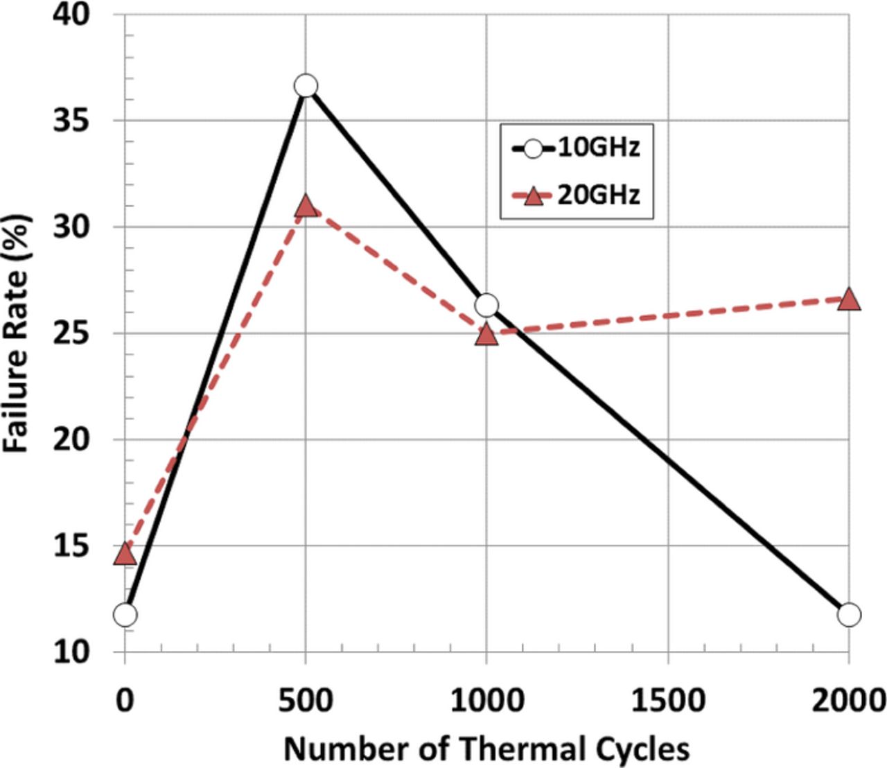
Figure 7. Reliability analysis data showing the relationship between failure rate and the number of thermal cycles at frequencies of 10 and 20 GHz.
This is further supported by the multiple slopes in the cumulative failure plots for 10 GHz (Figure 8a) and 20 GHz (Figure 8b) respectively. The distributions of the data show at least three different slopes, at both frequencies. This suggests competing failure modes and mechanisms within the TSV in response to the stress buildup from the thermal cycling.11 Identifying and resolving these competing mechanisms is the subject of current ongoing research.
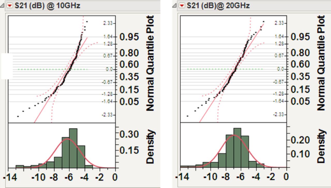
Figure 8. Statistical analysis showing the distribution of all the data points, and are presented as normal quantile and histogram plots at (a) 10 GHz and (b) 20 GHz, respectively.
Conclusions
In this paper, we have described the failure mode information inherent in high frequency electromagnetic signal loss data. Specifically, we have shown that it is possible to probe material and structural changes in integrated circuits under various external perturbations with broadband RF, as well as to detect buried artifacts. Additionally, the RF-based techniques described here provide several pieces of information, which when taken together provide a more complete picture of the progressive defect growth in the devices under test.
The impact of external perturbation on the reliability of 3D-ICs can be deduced from the resultant changes in the device impedance, through changes in the signal propagation characteristics (e.g., insertion losses and signal velocity). For example, changes in insertion loss above 20 GHz as a function of thermal cycling point to the formation of defects such as cracks and delamination at the bulk Cu-fill–isolation liner interface. Also, changes in the signal velocity suggest the coalescing and migration of small voids in the dielectric away from the copper fill, toward the silicon substrate. In the extreme, this migration could result in interfacial de-bonding and allow current leakage into the silicon substrate.
Finally, we have demonstrated that the S11 data from SMM technology can detect in-service material changes, such as degradation and corrosion of metal lines.
Footnotes
- c
Certain commercial equipment, instruments, or materials are identified in this report in order to specify the experimental procedure adequately. Such identification is not intended to imply recommendation or endorsement by the National Institute of Standards and Technology, nor is it intended to imply that the materials or equipment identified are necessarily the best available for the purpose.
- d