Abstract
The optimization of the porosity and pore radius of ZnO for the application in dye-sensitized solar cells is essential to enhance the cell performance. Porous ZnO films were fabricated by electrodeposition in the presence of eosin Y or in combination with eosin B which was used as a structure directing agent (SDA) for the first time. The influence of the deposition time and the SDA concentration on film porosity and pore radius was characterized by a combined electrochemical and atomic absorption spectroscopy analysis, and confirmed by gas sorption, optical spectroscopy and scanning electron microscopy. The combination of eosin Y with eosin B as SDA results in porous ZnO films with larger pore radius compared to the films prepared with eosin Y only. The larger pores showed a significantly decreased diffusion impedance leading to an increased photocurrent less hindered by mass transport. Successful application of these new ZnO films in dye-sensitized solar cells confirmed improved pathways for large complex ions as redox shuttles through the ZnO pore structure.
Export citation and abstract BibTeX RIS

This is an open access article distributed under the terms of the Creative Commons Attribution Non-Commercial No Derivatives 4.0 License (CC BY-NC-ND, http://creativecommons.org/licenses/by-nc-nd/4.0/), which permits non-commercial reuse, distribution, and reproduction in any medium, provided the original work is not changed in any way and is properly cited. For permission for commercial reuse, please email: oa@electrochem.org.
Dye-sensitized solar cells (DSSCs) are of interest as an alternative to established silicon-based solar cells owing to their potential to include materials which are readily available, environmentally friendly and can be prepared by low-cost techniques.1 For an efficient DSSC the interplay of the different involved materials, namely porous semiconductor, dye and redox mediator, is of high importance2,3 and has to be optimized following replacement of one of the components.
The requirements of a redox mediator, e.g., are on the one hand the fast dye regeneration at low overpotential and on the other hand a slow recombination with electrons in the conduction band of the semiconductor. The latter can be considered the main reason for use of the redox couple iodide/triiodide for a long time in DSSCs despite the disadvantages of iodide/triiodide such as the corrosion of the metallic counter electrode and a high overpotential needed for dye regeneration limiting the open-circuit photovoltage (Voc) that can be reached.4,5 Because of these disadvantages alternative redox couples are required to further improve the DSSC efficiency. Cobalt-based and copper-based complexes have been found to be suitable in such strategy.5–8 By variation of ligands the redox potential can be adjusted well to the potential required to reduce the oxidized dye in regeneration of the dye to enhance the performance of the solar cells.9,10 Such change of the redox mediator, however, poses new challenges to cell performance and asks for proper adjustments in the pore structure of the semiconductor electrode. A high surface area is needed generally in DSSCs to reach a high dye loading and, therefore, high photocurrents.1 Samples with such high surface area, however, tend to provide narrow pores, only. Narrow pores, on the other hand, can lead to lowered photocurrents in DSSCs if the diffusion of redox mediators becomes rate-limiting which can easily happen for ions as large as the copper-based or, in particular, the cobalt-based complexes.11 Poor fill-factors can result from such increased diffusion impedance. To allow for a good diffusion of these large complexes through the photoelectrode and hence, to enable improved efficiencies of DSSCs large pore radii have to be established.
Aside from the well-established TiO2, ZnO was shown to be a promising photoelectrode material considering the faster charge transport with a higher electron mobility which potentially can lead to enhanced DSSC efficiency.12,13 ZnO can be prepared by a variety of methods such as sol-gel processes, physical vapor deposition or electrochemically triggered electrodeposition reactions.14–16 Films can be, e.g., obtained easily from aqueous solutions at low temperature by electrodeposition using various substrate geometries, even microstructures, wires or textiles aside from established glass or light-weight and flexible polymer substrates.17–19 The presence of structure directing agents (SDA) which are added into the deposition bath to control the ZnO deposition leads to the desired porosity of ZnO films.20,21 However, mass transport in DSSCs with ZnO is attenuated by the narrow pore system in ZnO electrodeposited in the established way, requiring further improvements of the ZnO pore network.22 Typically organic dyes or surfactants are applied as SDA by linking their characteristic groups like, e.g., acid functions to the growing zinc oxide crystals or by the formation of aggregates on the substrate surface which then can influence the ZnO growth.23,24
In the present work, porous ZnO films were prepared via electrodeposition with addition of different SDAs. Apart from the well-established molecule eosin Y (EY) a related molecule eosin B (EB) or mixtures of the two have been used for the first time. The porosity and the pore radius of the deposited ZnO films were determined by a combination of atomic absorption spectroscopy (AAS), electrochemical impedance spectroscopy (EIS) and Brunauer-Emmett-Teller (BET) analysis and the dependence on deposition conditions was discussed. The best deposition conditions were chosen for the electrodeposition of highly porous ZnO films with good adhesion to the substrate and large pores to obtain suitable materials for application as photoanode material in DSSCs. Current-voltage curves of the produced solar cells, EIS and intensity modulated photocurrent spectroscopy (IMPS) were performed to investigate the effect of the SDA on the porous ZnO films in terms of electron transport within ZnO and ion transport in the pore system.
Experimental
Substrate pre-treatment
FTO-coated glass substrates (Kaivo, <15 Ohm sq−1) were cut and subsequently cleaned with RBS solution (Roth), acetone (Roth, ≥99.5%) and isopropanol (Roth, ≥99.8%) in an ultrasonic bath at room temperature for 15 min, respectively. The cleaned substrates were exposed to 5 mM aqueous KMnO4 solution (Roth, ≥99%) with 0.25 vol% n-butanol (Roth, ≥99.5%) for 20 min at 80–85°C to create MnO(OH) nucleation seeds as described in Ref. 25. Thereafter, the substrates were rinsed with distilled water (≤3.0 μS cm−1) and cleaned in an ultrasonic bath for 5 min.
Electrodeposition of ZnO thin films
The electrochemical deposition of ZnO was carried out from an aqueous solution of 0.1 M KCl (Aldrich, ≥99.5%) and 5 mM ZnCl2 (Merck, ≥98%) at 70°C while bubbling with O2 (Praxair, ≥99.5%) and using a three electrode setup as reported in Ref. 17. The pre-treated substrate was mounted to a rotating disk electrode (BELLTEC) and served as the working electrode. A platinum wire was used as the counter electrode and the reference electrode was a Ag/AgCl electrode (REF201 Red Rod, Radiometer analytical). First, a compact ZnO film was deposited at a constant applied potential of −1060 mV for 600 s for electrochemical measurements or 200 s for atomic absorption spectroscopy measurements. The thickness of the compact film remains in the range of the desired value (average thickness of 592 nm with standard deviation of 41 nm) as shown in Figure S1 for the films electrodeposited for 600 s. A planar and uniform film surface is confirmed by a small rms-roughness of the film of around 40 nm measured by confocal laser microscopy.
For the subsequent deposition of mesoporous ZnO films onto the compact layer a zinc wire served as the counter electrode, EY (Chemplex, >88%) as well as EB (Aldrich, >95%) were added at concentrations of 0–50 μM to the deposition bath and the deposition was continued at −960 mV at deposition times of 20–50 min. Afterwards, the samples were placed in a KOH solution with a pH of 10.5 at 70°C and slowly allowed to cool down to room temperature. To fully desorb EY and/or EB out of the ZnO films the samples were stored overnight in fresh KOH solution22 under white light illumination, rinsed with distilled water and ethanol and finally dried with N2 gas. The latter provided a convenient test of film adhesion.
Sample characterization
The surface morphology of the deposited films as well as the sample cross section were analyzed by scanning electron microscopy (SEM) in a Zeiss MERLIN at an emission current of 100 pA and an acceleration voltage of 5 kV. The thickness of the compact and the porous parts of the ZnO films was determined by using an Alpha-Step profilometer by Tencor Instruments. After bake-out at 120°C for 12 hours, BET analysis of selected ZnO films was performed as reported in Ref. 26 to determine the surface area in a Quantochrome Autosorb iQ at 77 K using Krypton as adsorbate.
The electrochemical capacitance of the ZnO films was measured in a 0.1 M aqueous KCl solution using an IviumStat potentiostat/galvanostat. To remove dissolved oxygen from the solution, N2 gas was supplied into the solution before and during the measurements. The ZnO working electrode was placed in the solution with a platinum wire counter electrode and an Ag/AgCl reference electrode. The capacitance was determined by scanning from 0.6 V to −1.0 V at a constant frequency of 0.1 Hz and an amplitude of 0.01 V. For control purposes, a broader frequency range from 1000 to 0.1 Hz at a bias potential of −1.0 V was also measured. To confirm that the ZnO films did not significantly alter during the electrochemical measurements, cyclic voltammograms were measured immediately before and following the impedance characterization. The cyclic voltammograms revealed just subtle changes as shown in Figure S2 indicating that the ZnO films remained stable during the characterization process.
The amount of ZnO in the porous films was determined by measuring the total concentration of zinc using AAS (Perkin Elmer Aanalyst 300) after dissolving the respective ZnO film in 20 mL of 0.2% HNO3 solution overnight. To obtain the ZnO amount of the porous part of the films only, the ZnO amount of a compact film was determined separately and substracted from the measured value of the samples.
Mounting and analysis of the films in DSSCs
Sensitization of the ZnO films was carried out as described earlier.27 The deposited ZnO films were heated at 150°C for 1 h and placed under UV irradiation for 30 min to hydroxylate the ZnO surface.28 Thereafter, the samples were placed into a solution containing 0.5 mM of the indoline sensitizer DN216 and 1 mM lithocholic acid (Aldrich, ≥97%) in tert-butanol (Roth, ≥99.5%) and acetonitrile (Roth, ≥99.9%) at a volume ratio of 1:1 for 15 min and rinsed afterwards with ethanol to remove excess dye and finally dried in air. Diffuse transmission spectroscopy of sensitized ZnO films was performed employing a tec5 UV/Vis spectrometer and an Ulbricht sphere behind the sample to collect all transmitted as well as forward-scattered light.
Poly(3,4-ethylenedioxythiophene) (PEDOT) served as the counter electrode and was prepared as reported earlier.29 PEDOT was galvanostatically deposited on FTO-coated glass from an aqueous solution of 0.1 M sodium dodecyl sulfate (Aldrich, ≥99%) and 0.01 M 3,4-ethylenedioxythiophene (Aldrich, 97%) with a deposition current density of 0.2 mA cm−2 for 170 s. After the deposition the FTO/PEDOT electrode was rinsed with distilled water and dried in air.
Two different redox electrolytes containing cobalt or copper complexes were used in DSSCs. The composition of the electrolytes was either 0.23 M Co(bpy)3(PF6)2 (Dyenamo, 99%), 0.07 M Co(bpy)3(PF6)3 with bpy = 2,2'-bipyridine, 0.1 M LiTFSI with TFSI = lithium bis(trifluoromethane)sulfonimide and 0.4 M TBP with TBP = 4-tert-butylpyridine or 0.2 M Cu(tmby)2TFSI (Dyenamo, 95%), 0.04 M Cu(tmby)2(TFSI)2 with tmby = 4,4',6,6'-tetramethyl-2,2'-bipyridine, 0.1 M LiTFSI and 0.4 TBP in acetonitrile.
The sensitized ZnO electrode was assembled with the PEDOT counter electrode by a hot-melting Surlyn sealant foil (thickness: 25 μm) as described in Ref. 30. The electrolyte was introduced through pre-drilled holes in the counter electrode. To avoid evaporation of the electrolyte the holes were covered with a coverslip of glass and sealed with Surlyn foil.
Current-voltage characteristics were measured by a Zahner IM6 potentiostat in the dark or under illumination with a LOT-Oriel 150 W Xenon arc lamp with an AM 1.5 G filter and a calibrated intensity of 100 mW cm−2. A mask with a circular opening of 7 mm diameter was placed in front of the cell to expose the active area only and minimize light scattering by the glass surface. Impedance measurements were performed under identical illumination and at open-circuit condition with the Zahner IM6 potentiostat in a frequency range from 100 kHz to 300 mHz and an amplitude of 10 mV. In addition, IMPS was carried out using a red LED (λ = 625 nm) under variation of the illumination intensity from 25 to 0.5 mW cm−2 at a modulation of 5% in a frequency range from 100 kHz to 300 mHz.
Results and Discussion
Dependence of pore structure on deposition time
The addition of EY or EB as structure directing agents significantly transforms the morphology of electrodeposited ZnO from a compact structure with hexagonal crystallites in their absence into a mesoporous structure as shown in Figure 1. The influence of the deposition time on the column and pore radius were directly observed by SEM. The morphology of porous ZnO deposited for different deposition times of a given EY concentration (50 μM) are depicted in Figures 1a and 1b. It is seen that longer deposition time leads to larger pores in the ZnO films and an increasing column radius which is also indicated by increased light scattering of the films (Figure S3) as commonly observed for semiconductor films consisting of large particles.31 Increased scattering by an increased film thickness only should be of minor relevance as shown earlier for TiO2 films where doubling of the film thickness at constant pore size resulted in a negligible change in light transmission.31
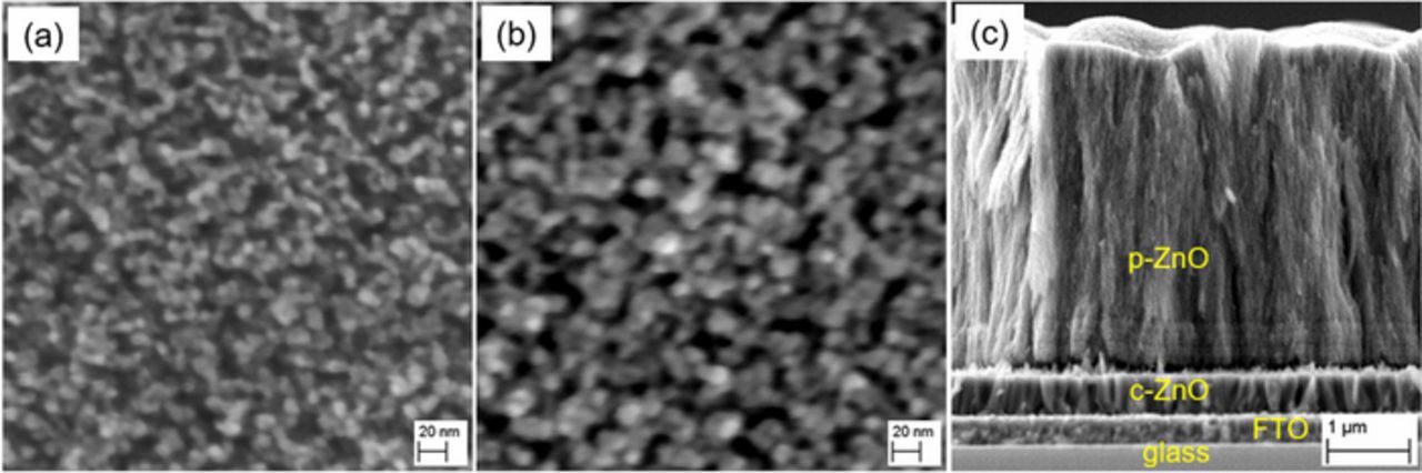
Figure 1. Porous ZnO deposited in the presence of 50 μM EY for 20 min (a) and for 40 min (b), cross-section of a ZnO sample deposited in the presence of 50 μM EY and 50 μM EB for 20 min (c).
As the examination by SEM only gives a rough indication about the size of the pores more precise values for the porosity P and the average pore radii rpore were obtained from independent measurements. The absorption spectrum of a ZnO film (Figure S4) after KOH treatment clearly shows no peak that could be assigned to eosin. Hence, we conclude that eosin could be fully desorbed from the film and no pores have been closed off within the film. P was obtained from the porous film volume Vfilm and the volume Vs occupied by ZnO according to Equation 1. Vfilm was calculated from the geometric area of the film and the film thickness measured by profilometry. Vs was determined from the mass of ZnO in the porous film obtained by atomic absorption spectroscopy following dissolution of films. For atomic absorption spectroscopy measurements, a thin compact ZnO film was prepared by electrodeposition for 200 s to minimize the error for the measured Zn amount from the compact layer and still allow the deposition of mesoporous films with sufficient adhesion on the compact layer. However, in order to obtain a completely closed compact ZnO film for the photoelectrochemical characterization the deposition time for the compact film was increased to 600 s.
![Equation ([1])](https://content.cld.iop.org/journals/1945-7111/166/9/B3040/revision1/d0001.gif)
In the cross section of the ZnO samples tube-like features can be observed by SEM extending throughout the film normal to the substrate as shown in Figure 1c indicating cylindrical pore geometries with a volume Vcyl = π r²pore h and a surface area Scyl = 2 π rpore h with h being the thickness of the porous ZnO. rpore was determined as shown in Equation 2 from the ratio of the total pore volume Vpore = Vfilm−Vs = P Vfilm in a given film (see Equation 1) and its overall surface area S determined by capacitance measurements. The ratio of the Helmholtz double layer capacitance Ch and a reference capacitance Cref provides a good measure for S.32 The value for Cref corresponds to the capacitance of an ideal flat ZnO film which has been taken from Ref. 32 for further calculations. Ch of the samples was determined by capacitance measurements.
![Equation ([2])](https://content.cld.iop.org/journals/1945-7111/166/9/B3040/revision1/d0002.gif)
Figure 2a shows a typical capacitance-potential curve of ZnO in aqueous KCl solution. At negative potentials close to −1.0 V the capacitance saturates which can be observed properly in Figure 2a and the Helmholtz double layer capacitance Ch dominates.33,34 To determine rpore the Helmholtz double layer capacitance value at a potential of −1.0 V has been taken from the capacitance-potential curves. Measuring at more negative potentials led to degradation of the films.
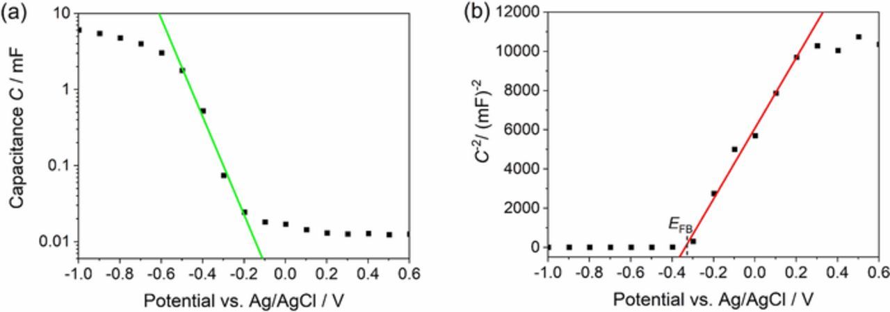
Figure 2. Capacitance C against potential (linear fit → chemical capacitance (green)) (a) and Mott-Schottky curve (linear fit → Mott-Schottky capacitance (red)) with the flatband potential EFB (b) of a porous ZnO film on compact ZnO and FTO-coated glass in 0.1 M aqueous KCl solution measured at 0.1 Hz.
The thickness of the deposited films was necessary to calculate rpore as shown in Equation 2. It can be seen in Table S1 that the films persistently became thicker at longer deposition times, as expected. The values for the capacitance Ch also increased but less steeply than the film thickness. Interestingly, doubling the deposition time leads to a twice as thick film but the capacitance Ch is far from being doubled indicating an increasing pore radius during film growth.
At less negative potentials the typical exponential correlation between the chemical capacitance Cμ in ZnO and the potential is observed as seen in Figure 2a.33–35 At positive potentials the capacitance of the compact ZnO follows the Mott-Schottky equation typical for the space-charge capacitance of a semiconductor electrode and plotting C−2 against the potential shows a linear behavior.34 The flatband potential for the films is estimated from the plot to about −0.34 V indicated by the dotted line in Figure 2b which fits well with the value reported in Ref. 36. A more detailed analysis as proposed in Ref. 37 to separately characterize the trap states energy was omitted to allow comparison of the data to the reference value.
The values for rpore and P of ZnO determined from capacitance measurements, film thickness and AAS analysis were plotted against the deposition time as shown in Figure 3a. rpore exhibits a linear increase with longer deposition time whereas P stays widely constant which is confirmed by a constant ratio of deposition charge and film thickness (Table S1). The calculated values for rpore increase from 4.4 ± 0.2 nm after 20 min to 8.0 ± 0.5 nm after 50 min whereas P stays widely constant in a range from 47.0 ± 2.0% (40 min) to 53.9 ± 1.4% (30 min).
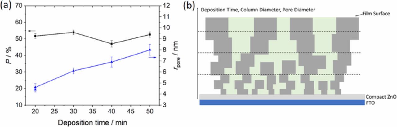
Figure 3. Porosity P and pore radius rpore of the porous ZnO films after different deposition times (a), scheme of the film structure with pores (green) and ZnO columns (gray) (b).
Extrapolating the values of rpore to a deposition time of 0 min leads to a pore radius of 2 nm which stands for the pore radius in the beginning of the porous film growth and is in the range of the size of eosin molecules or aggregates. Such increasing pore radius at constant P, further, indicates an increasing diameter of the ZnO columns at longer deposition times, as schematically shown in Figure 3b and as also seen for other examples by a suppressed growth of narrow columns at prolonged deposition times.38,39 A nearly constant overall growth rate of ZnO during the deposition process can be derived from a widely constant deposition current. In Ref. 40 a saturation of the ZnO thickness at about 8 μm was reached for longer deposition times caused by a self-limitation of the ZnO growth process which, however, was not reached by the chosen short deposition times in the present study.
As a resume, longer deposition times with a constant concentration of eosin lead to a constant porosity, an increase in the column diameter and pore radius and a decreasing surface area of ZnO (Figure 3b).
Influence of EY concentration on porosity and the role of EB
The influence of the eosin concentration on the porosity and the pore radius of deposited ZnO was investigated utilizing either pure EY, pure EB or a combination of EB and EY. Cyclic voltammograms of both eosin species in 0.1 M KCl solution were, therefore, measured to compare their redox potentials and discuss their role as SDA. The measured cyclic voltammograms for both eosin species are shown in Figure S5.
The reduction wave for EY is found at −0.83 V and the oxidation wave at 0.85 V which correspond well to reported values.41 EB shows a reduction wave at −0.66 V and an oxidation wave at 1.10 V. Both the reduction as well as the oxidation potentials for EB, therefore, are shifted to positive potentials by about 200 mV compared to EY. The strongest influence of EY on the porosity of ZnO was found when ZnO electrodeposition was performed at potentials where EY is reduced.42 Since EB is reduced already at −750 mV it should lead to porous ZnO films even at this deposition potential. Such experiments were performed and the expectation was clearly confirmed by SEM (Figure S6). At −960 mV, however, both EB and EY are in their reduced state and should both contribute to the pore structure of the deposited ZnO films by formation of complexes of reduced eosin species and Zn2+ ions.23 Therefore, the films deposited in the presence of both EY and EB were deposited at −960 mV. The influence of the eosin concentration on the pore structure of ZnO was analyzed in the presence of EB and different EY concentrations for a fixed deposition time of 20 min.
The measured film thickness and the Helmholtz double layer capacitances of each film are shown in Figures 4b and 4c. The films become thicker with higher eosin concentration whereas the values for the Helmholtz double layer capacitance remain in a similar range. The growth rate of ZnO increases with the eosin concentration as seen by the increase of the film thickness at a constant deposition time.21
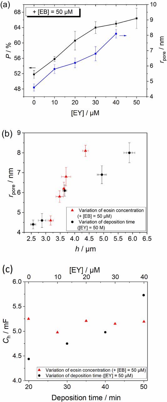
Figure 4. Porosity P and pore radius rpore of the porous ZnO films in relation to the EY concentration additional to 50 μM EB (a), rpore as a function of the ZnO film thickness h with variation of the eosin concentration at a constant deposition time (red) or variation of the deposition time (black) (b), Helmholtz double layer capacitance Ch as a function of the eosin concentration (red) and the deposition time (black) (c).
Plotting P and rpore against the concentration of EY (Figure 4a) indicates a rise of both unlike the case of different deposition times (Figure 3a). P rises from 51.8 ± 1.0% to 66.4 ± 2.7% whereas values for rpore vary from 4.6 ± 0.2 nm to 8.1 ± 0.3 nm. The increase of P is explained by a dominant tendency of eosin to inhibit ZnO growth by occupying active spots with eosin molecules and aggregates21 which preferentially form and grow to larger size within the electrodeposited film at higher concentration of eosin in the deposition bath. Therefore, an increased concentration of EY and EB leads to higher P with larger pores, as also observed earlier for EY as single SDA.21 The almost constant values for the capacitance correspond to a widely unchanged surface area of the mesoporous ZnO (Figure 4c) which can be explained (Equation 2) by a compensation of an increase of P (Figure 4a) and film thickness (Table S1) by significantly increased pore radii (Figure 4a).
We note that for an increasing amount of eosin in the deposition bath an increase in film thickness is observed for a given deposition time (Figure 4a). To distinguish between an enlargement of pores for thicker films as in Figure 3 and a possible effect of eosin concentration, rpore is plotted versus h in Figure 4b. It is clearly seen that rpore is more strongly influenced in its relation to h by the eosin concentration at a fixed deposition time than by the deposition time at a fixed eosin concentration. For two samples with similar film thickness but deposited at either different deposition time or at different eosin concentration an enlargement of the pores with higher SDA concentration can be concluded. Larger pores can be formed for moderately thick films at higher eosin concentration.
During drying of the films by blowing a stream of nitrogen it was observed that the films prepared in the presence of EB did stick better to the substrate than films prepared with EY only. As one reason for the exfoliation of freshly prepared ZnO/EY films a shrinking volume of the complex consisting of Zn2+ and reduced EY23 upon reoxidation of EY during film conditioning in KOH was assumed.43 In earlier work42 it was found that the redox state of EY (neutral or reduced) had a clear influence on its role as SDA in the formation of pores in ZnO. The reoxidation of eosin occurs after the as-deposited ZnO films come in contact with air.20 Reduced EB or complexes of reduced EB and Zn2+ are less easily oxidized to the neutral form than found for EY21,23 leading to slower shrinkage and, therefore, improved adhesion of ZnO films formed during simultaneous desorption of EY and EB.
Values of the surface areas of selected porous ZnO films obtained from Ch (Equation 2) were confirmed by two independent methods as shown in the supplementary information. Controlled adsorption of EY to the porous films following conditioning and measuring the absorbance spectra of the films (Figure S4) led to absorbance values which are quite independent of the concentration of eosin during deposition speaking in favor of a constant surface area. This conclusion is directly supported by the nearly constant BET surface as well as by constant values of the Helmholtz double layer capacitance (Figure S7).
Influence of porosity and pore radius on charge transport in DSSCs
In order to apply ZnO as electrode in DSSCs, an optimum choice of the concentrations of EY and EB was made to obtain ZnO films with a high porosity, large pores and good adhesion to the substrate. Such films were deposited from solutions of 50 μM EB and 30 μM EY at a deposition potential of −960 mV. DSSCs from such films were compared to cells from ZnO films deposited in the presence of 50 μM EY as in Ref. 30. The characteristic parameters for the ZnO films and DSSCs are listed in Table I.
Table I. Deposition parameters, film thickness h of the deposited porous ZnO films, redox mediators and cell parameters of the fabricated DSSCs. P* and rpore* correspond to the determined values of equivalent samples.
| SDA (deposition time) | h/μm | P*/% | rpore*/nm | Redox mediators | η/% | Jsc/mA cm−2 | Voc/V | FF |
|---|---|---|---|---|---|---|---|---|
| EY (25 min) | 3.12 | 51.7 | 4.4 | Co(bpy)3 | 3.32 | 10.69 | −0.535 | 0.583 |
| EY/EB (20 min) | 3.47 | 64.0 | 6.9 | Co(bpy)3 | 3.44 | 10.45 | −0.532 | 0.619 |
| EY (25 min) | 3.14 | 51.7 | 4.4 | Cu(tmby)2 | 3.01 | 9.04 | −0.734 | 0.454 |
| EY/EB (20 min) | 3.86 | 64.0 | 6.9 | Cu(tmby)2 | 3.43 | 9.60 | −0.728 | 0.491 |
As shown in Figure S8 for all DSSCs containing either Co(bpy)3 or Cu(tmby)2 electrolytes current-voltage characteristics of well-performing DSSCs could be obtained. As a result of the more negative redox potential of the copper complex8,44 the values for the open-circuit voltage Voc of the cells with the Cu(tmby)2 electrolyte are 0.2 V higher than with the Co(bpy)3 electrolyte. It can be seen that the slope of the current-voltage curves at more negative potentials is different depending on the employed electrolyte caused by the different diffusion impedance of the electrolyte. The reduced slope for the cells containing the Cu(tmby)2 electrolyte indicates higher diffusion impedance and hence a slower diffusion of copper redox species in the electrolyte leading to a lower fill factor.30
The solar cells based on ZnO grown in the presence of both EY and EB (ZnOEY/EB) deliver slightly higher efficiencies and fill factors, especially in contact with the Cu(tmby)2 electrolyte compared to ZnO films prepared under established conditions (ZnOEY). EIS served to analyze cell characteristics in more detail. The measured data were fitted using the equivalent circuit depicted in Figure S9 which has been described in detail in Ref. 22. When using the Co(bpy)3 electrolyte two maxima are observed in the Bode plot as shown in Figure 5. The maximum at about 100 Hz can be assigned to a superposition of an impedance originating from both, the diffusion of electrons in the porous ZnO film and the back reaction of electrons with the oxidized redox species in the electrolyte with the recombination resistance Rrec and the chemical capacitance Cμ at the ZnO-electrolyte interface.45 The maximum at about 2 Hz is caused by diffusion of the redox species in the electrolyte characterized by the diffusion impedances Zd,WE at the ZnO side and Zd,CE at the counter electrode side.22
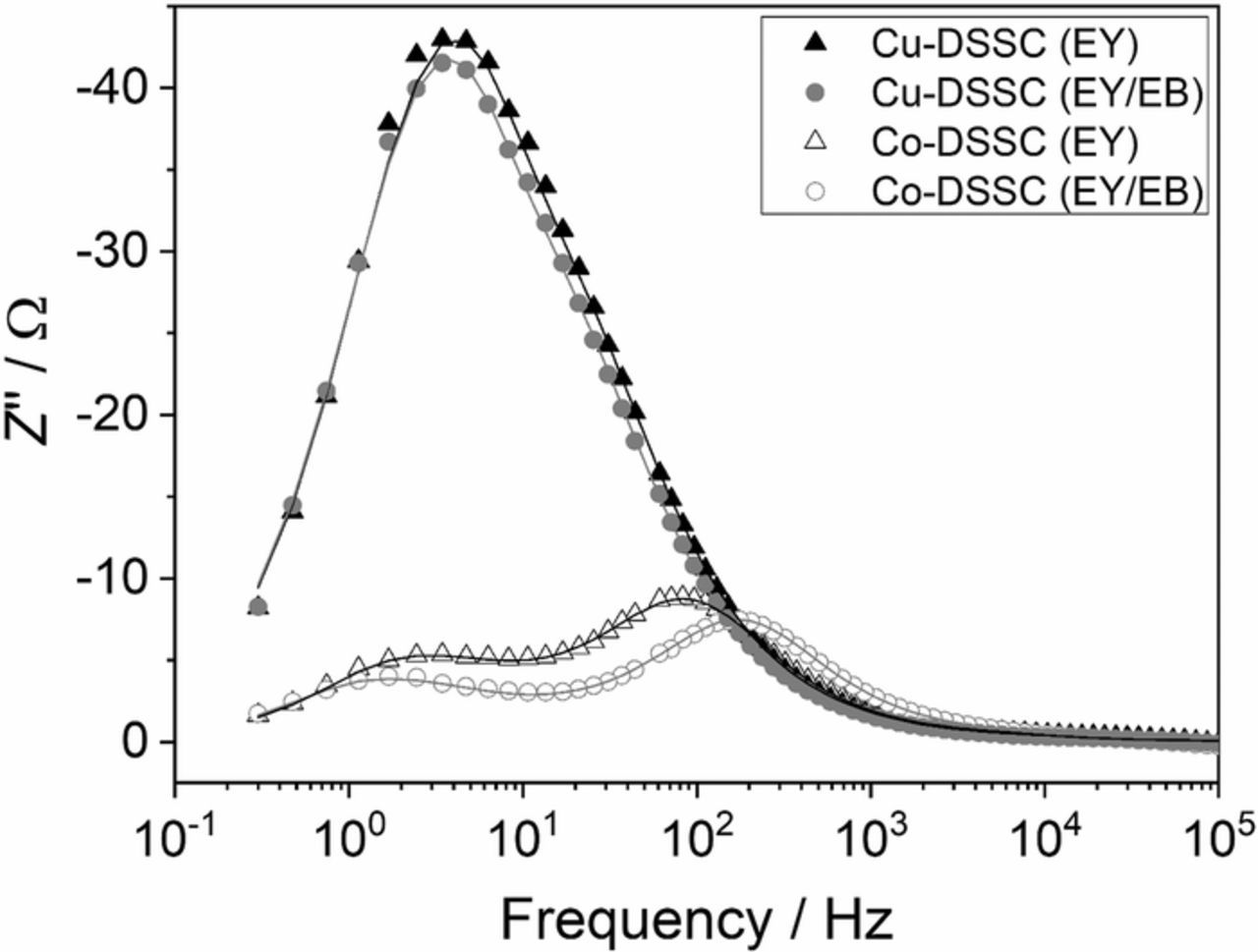
Figure 5. Bode plot of DSSCs with the Co(bpy)3 and Cu(tmby)2 electrolytes and ZnO prepared with either EY or EY/EB.
Application of the Cu(tmby)2 electrolyte in the solar cells results in an overlap of all these maxima so that only one peak is observable in the Bode plot at about 3 Hz (Figure 5). The overall impedance obviously is dominated by the diffusion of the redox species in the electrolyte (Zd,WE and Zd,CE) which are significantly higher than in the cells with the Co(bpy)3 electrolyte. This can be caused by the presence of TBP in the electrolyte slowing down the diffusion rate of the copper complexes by formation of a spatially more demanding coordination shell of Cu(II) by ligand exchange with TBP.10 The reaction of Cu(II)(tmby)2 with TBP to Cu(II)(TBP)4+x(ACN)y2+ leads to a larger complex and, therefore, to slower diffusion as directly seen by the higher impedance.
Since no separate maxima exist in the Bode plot of the solar cell containing the Cu(tmby)2 electrolyte, the recombination resistance, chemical capacitance and the total diffusion impedance Ztotal = Zd,CE+Zd,WE can be determined more reliably for the cells using Co(bpy)3. The total diffusion impedance (Table II) of the redox species in ZnOEY/EB is remarkably smaller compared to the reference cell ZnOEY which is consistent with the higher porosity and larger pore radius of the ZnOEY/EB films.
Table II. Vs/S values and characteristic parameters of the DSSCs with Co(bpy)3 electrolyte and ZnO deposited with EY or EY/EB by fitting with ZView.
| SDA | ZnOEY | ZnOEY/EB |
|---|---|---|
| Vs/S/10−7 cm³ cm−2 | 2.06 | 1.92 |
| Rrec/Ω | 17.02 | 14.93 |
| Cμ/mF | 0.130 | 0.073 |
| Rrec Cμ = τe/ms | 2.08 | 1.09 |
| Ztotal/Ω | 12.17 | 9.94 |
The electron lifetime46 τe = Rrec Cμ (Table II) for the solar cell from ZnOEY/EB is about half the value of the reference cell which corresponds well to the smaller open-circuit voltage using ZnOEY/EB. The reason for the short electron lifetime can be understood from its dependence on the ratio of Vs/S as described in Ref. 45 where τe was found to be proportional to Vs/S. The small value Vs/S for the ZnO film prepared with EY and EB resulting from a higher porosity and larger pores is found smaller than for ZnOEY but the rather small difference alone cannot explain the considerably smaller τe found for ZnOEY/EB. Another explanation could be the increased presence of defects leading to a change of the surface states and therefore to a smaller τe.
The transit time τtr and the diffusion coefficient Dn of electrons in ZnO as a function of the short-circuit current were determined from IMPS measurements (Figure S10). For this purpose, the frequency of the minimum of the imaginary part of the photocurrent was determined leading to τtr = 1/(2 π fIMPS) and Dn = h²/(γ τtr) calculated using the factor γ = 2.7747 and the film thickness h. It becomes clear that ZnOEY/EB with a higher porosity and larger pores provides a more narrow pathway of electrons through the ZnO network of the electrode leading to a smaller Dn.
Although the solar cell with ZnOEY/EB shows a shorter electron lifetime and a longer transit time for the charge transport of the electrons, the charge extraction efficiency is still reasonably high resulting in a short-circuit current comparable to the reference solar cell with ZnOEY. Hence, the diffusion of the redox species in the electrolyte provides the dominant contribution to the improved properties of the solar cell, mainly reflected in an increased fill factor.
In summary, a faster diffusion of the large redox species through the ZnO pore system was established by increased porosity and pore size in ZnOEY/EB which hopefully can be exploited more vigorously in future cells employing more steric sensitizers and/or redox mediators.
Conclusions
In this work, porous ZnO films were prepared by electrodeposition in the presence of both eosin Y and eosin B. Their presence under variation of the deposition time leads to larger pores and a constant porosity. An increasing eosin concentration at a constant deposition time resulted in larger pores and higher porosities. It becomes clear that the average pore radius can be controlled by adjusting the deposition time as well as the eosin concentration whereas the porosity depends on the eosin concentration only. The ZnO films prepared in the presence of eosin B and eosin Y as SDA with such increased porosity and pore size were tested in dye-sensitized solar cells leading to facilitated diffusion of the redox species in the electrolyte through the more open pore structure of the ZnO photoelectrode.
Acknowledgments
We are grateful for financial support by the Deutsche Forschungsgemeinschaft (DFG) via the project "SCHL340/19-1" and via the GRK 2204 "Substitute Materials for sustainable Energy Technologies" as well as to the group of B. Smarsly for the BET analysis, the group of B. Spengler for the AAS measurements and H. Miura (Chemicrea Co, Japan) for providing the dye DN216.
ORCID
Derck Schlettwein 0000-0002-3446-196X