Abstract
The article aims to optimize the inkjet printing properties to realize highly conductive and mechanically stable printed patterns on the Polyethylene terephthalate (PET) substrate. The key printing parameters such as drop spacing, the number of printed layers, and sintering temperatures were investigated. The test specimens were printed using silver nanoparticle ink and Dimatix 2831 inkjet printer. Then, the printed samples were characterized by electrical conductivity, bending, and adhesion tests. The Analysis of Variance (ANOVA) analysis showed that the number of layers and sintering temperatures were significant factors (p < 0.05) affecting electrical conductivity. The optimum printing parameters for the PET substrate were found to be 20 μm drop spacing, three layers of printing, and 120°C sintering temperature for 30 minutes. The measured optimum resistivity was found to be 5.25 μΩ-cm. The repetitive bending and adhesion test and ASTM tape test indicated good mechanical stability.
Export citation and abstract BibTeX RIS

This is an open access article distributed under the terms of the Creative Commons Attribution 4.0 License (CC BY, http://creativecommons.org/licenses/by/4.0/), which permits unrestricted reuse of the work in any medium, provided the original work is properly cited.
Implementation of flexible electronics is of significant interest because of its rapidly expanding market poised to reach $200 billion by the next ten years.1 Inkjet printing is a simple and cost-effective method to fabricate electronic devices,2–8 unlike photolithography. It offers direct writing of complicated patterns by controlled ink deposition on the substrate surface. However, some challenges of inkjet printing include the requirement of high-quality ink and the quality of the substrate surface.9
Two types of ink are routinely used for the inkjet printing process: organometallic inks and metal nanoparticle inks.10 The metal nanoparticles inks are generally preferred as they impart high electrical conductivity. Copper (Cu),11 Gold (Au)12 and Silver (Ag)13 nanoparticle (NPs) based inks are typically used for inkjet printing. Commercially available AgNPs are cheaper ($17 per ounce) than the AuNPs ($1100 per ounce) and the CuNPs ($20 per ounce).14 Moreover, Ag ink is robust against oxidation.15 AgNP ink is composed of Ag particles, solvents, and capping agents.16 Sintering is essential to densify metal particles by removing the solvents and capping agents from the pattern. Further, sintering seems to improve the electrical conductivity of the pattern. The choice of substrate is critical to realize electronic devices using inkjet printing.
Polyethylene terephthalate (PET) and polyethylene naphthalate (PEN) are two common polymeric substrates used for inkjet printing of electronic devices.9,17 PET has lower Young's modulus than PEN and hence preferred for flexible devices.18 However, PET has a low glass transition temperature of below 150°C.19
Hence, the sintering temperature needs to be chosen carefully for the PET substrate as higher sintering temperatures and sintering time can cause deformation of the substrate while lower temperatures may not yield optimum electrical conductivity. To ensure high printing quality, it is required to optimize the printer parameters for the selected ink and substrate combination20 as different inks with varying viscosity and surface tension interact differently with the substrate. In prior studies, PET-based inkjet printing has been investigated with silver nanoparticle ink.19,21,22 However, few have accounted for the increased conductivity while optimizing the printing materials, printing time, post-process, and mechanical stability. In an earlier report,21 the study of the Ag inkjet printing on a PET substrate following a layer by layer approach was presented. However, the reported process requires longer time as well as a higher number of printing layers (fourteen layers) to achieve the conductivity. Fourteen layers involves a high consumption of ink, consumables, and printing time. A similar experiment was conducted in a different study without considering the flexibility and adhesion test.19,22
In this article, the optimum printing parameters such as drop spacing, the number of printed layers, and sintering temperatures were determined to print highly conductive and mechanically stable pattern on PET substrates. Consecutive multilayer printing and sintering process was followed to get the optimum conductivity. The printed samples were inspected to ensure pattern quality. Bending and adhesion tests were performed to confirm pattern flexibility and durability.
Experimental
Materials (ink and substrate)
Commercially available Ag nanoparticle ink was purchased from Novacentrix (Model JS-A102A). It is a water-based ink with specifications Ag content 40 wt%, viscosity 8 to 12 cp and surface tension 19–30 dyne/cm. The PET substrate used in this study was bought from Mitsubishi Paper Mills having a thickness of 135 ± 12 μm.23 The substrate is thermally durable up to 120°C. The A4 size PET film was cut out into the square shapes of 20 mm × 20 mm dimensions to print the designed shape of 10 mm × 10 mm.
Printing of test specimens
The Ag ink deposition on the PET substrate was performed using a Fujifilm Dimatix Materials Printer (DMP-2831). It is a drop on demand inkjet printer that offers precise printing using both 1 pL and 10 pL volume cartridges. In our experiment, we used 10 pL cartridges having 16 nozzles of diameter 21 μm that are driven by the piezoelectric element of the Dimatix printer. Initially, printing pattern of dimension 10 mm × 10 mm was designed using ANSYS EM software and uploaded to the DMP as a bitmap file.24
Table I shows the experimental printing parameters. The next step was to optimize the printing parameters for this ink and substrate combination. The primary target of optimizing the parameters is to create a uniform and straight drop at a velocity within the range of 6–10 m/s from the selected nozzles so that the jetted drops attach well on the PET surface.
Table I. Experimental printing parameters.
| Parameter | Value | Unit |
|---|---|---|
| Drop Spacing (DS) | 15, 20, 25 | μm |
| No of printing layers (L) | 1, 2, 3, 4 | - |
| Sintering Temperature | 75, 90, 120 | °C |
The drop watcher of Drop Manager Software of DMP allows to monitor the drops and measure the drop velocity. The parameters that control the printing quality are the jetting waveform, the jetting voltage, the jetting frequency, the cartridge temperature, the platen temperature (where the substrate is placed) and the resolution of the pattern.24,25 To generate optimum printing quality, these parameters were optimized after multiple test printing. Table II shows the optimal printing parameters used in this experimental investigation. Figure 1 shows the size of the designed pattern and printed sample.
Table II. Optimal printing parameters.
| Jetting Frequency | 4.4 kHz |
| Drop Size | 10 pL |
| Printing Print Height | 750 μm |
| Cartridge Temperature | 28°C |
| Platen Temperature | 30°C |
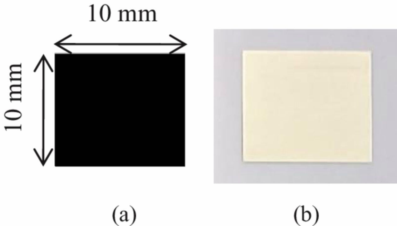
Figure 1. Size of the printing pattern.(a) Printing pattern, (b) Digital camera image of printed sample.
Post-treatments and resistivity measurements
To attain superior electrical conductivity after printing, the samples require sintering. Heat sintering helps the removal of solvent from the ink to form a conductive pattern.10 To investigate the relationship between conductivity, printing layers and sintering temperature, the samples were printed with single (1L), double (2L), triple (3L) and quadruple (4L) layers. The samples were cured at 75°C, 90°C and 120°C for 30 minutes on a digital hotplate (Model: HP88857100). The sintering temperature was kept up to 120°C to maintain the thermal compatibility of the substrate. For each experimental condition, five specimens were prepared and resistivity measured for each to obtain the average.
After curing the specimens on different temperature, the resistivity was measured using the formula:

Where Rs is the sheet resistance (Ω/sq) and t is the thickness of the Ag layer (μ-cm). The sheet resistance was calculated using Jandel's four-point probe and the thickness was measured using a Scanning Electron Microscope (Quanta 3D 200i).24
Flexibility and adhesion test
To implement flexible electronic devices, measuring bending and adhesion of the printed pattern is critical. In an earlier study,26 bending test was done with different radii of curvature to check the signs of permanent deformation or performance deteriorations. A similar approach was followed in our experiment. ASTM standard tape test was used to test the adhesion of printed specimens.
Characterization
The specimens were inspected using the CD microscope (Nikon MM-400) to investigate the uniformity of the printed pattern and surface morphology under multiple printing conditions. The thickness of the printed pattern was measured using the Scanning Electron Microscope (SEM) Quanta 3D 200i.
Results and Discussion
Figure 2 shows the microscopic images of the specimens printed with drop spacing of 15 μm (1693 DPI), 20 μm (1270 DPI) and 25 μm (1016 DPI). Sharp edge quality of the printed pattern at 20 μm DS was observed and compared to the DS 15 μm. The droplets were too close for 15 μm DS and they overlap each other.
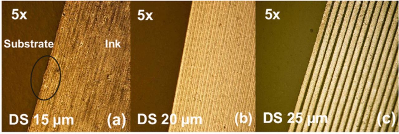
Figure 2. CD microscopic image (5x magnification) of Dimatix inkjet printed pattern with (a) 15 μm drop spacing, (b) 20 μm drop spacing, (c) 25 μm drop spacing.
On the other hand, higher DS (25 μm) created a discontinuous printed pattern characterized by high resistivity. Hence, the 20 μm DS was selected as the optimum DS. After determining the optimum DS, the correlation of resistivity with the number of printing layers and sintering temperature was studied. Table III shows the measured resistivity as a function of temperature and the number of printing layers. A statistical approach was followed to determine the significance of sintering temperature and the number of printing layers on the resistivity. Analysis of variance (Table IV) reveals that both the parameters significantly affect the resistivity. Larger F value for sintering temperature indicates its dominance over the printing layers in affecting resistivity.
Table III. Measured resistivity under experimental conditions.
| Resistivity (μΩ-cm) | ||||
|---|---|---|---|---|
| Temperature | 1L | 2L | 3L | 4L |
| 75 | 33.81 | 20.24 | 19.38 | 21.33 |
| 90 | 17.20 | 9.35 | 8.12 | 11.07 |
| 120 | 8.01 | 6.73 | 5.25 | 5.45 |
Table IV. ANOVA of the resistivity, temperature and number of printing.
| Source of Variation | SS | DF | MS | FCritical | F | P-values |
|---|---|---|---|---|---|---|
| Temperature | 635.03 | 2.00 | 317.51 | 37.45 | 5.14 | p < 0.05 |
| Number of printing layers | 141.22 | 3.00 | 47.07 | 5.55 | 4.76 | p < 0.05 |
| Error | 50.86 | 6.00 | 8.48 | |||
| Total | 827.11 | 11.00 |
Before sintering, the samples are non-conductive as it contains the solvent and Ag nanoparticles with a capping agent.16 After ink deposition, the solvent and capping agent need to be removed through sintering to ensure conductivity. Figure 3 shows the plot of electrical resistivity as a function of sintering temperature and the number of printed layers. The lowest resistivity value was found to be 5.25 μΩ-cm for 3L printing and 120°C heat-treatment. Figure 4 shows the microscopic image of the magnified surface of the 3L printed pattern. With increasing sintering temperature from 75 to 120°C, the particles get densified and form a well-connected conductive pathway (evident from the lower resistivity values). With the increasing number of printed layers, the thickness of the pattern increases (Table V).
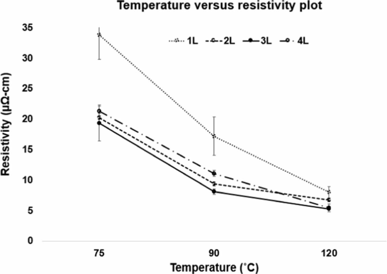
Figure 3. Resistivity values vs curing temperature plot for 1L, 2L, 3L and 4L of printing.
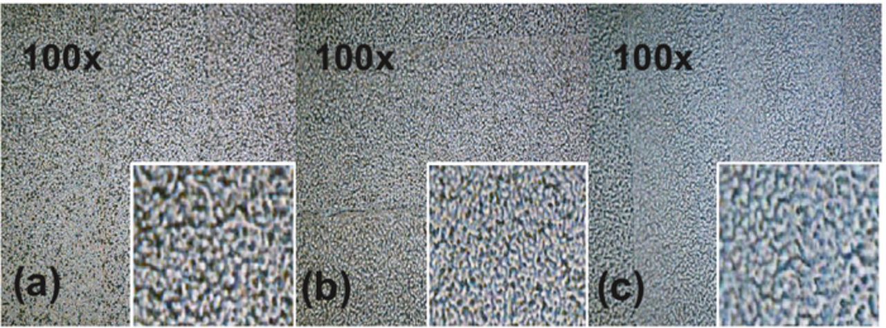
Figure 4. CD microscope image (100x magnification) of surface of 3L printed pattern at different temperature: (a) 75°C (b) 90°C (c) 120°C.
Table V. Thickness of the printed pattern.
| Layers | Thickness (μm) |
|---|---|
| 1L | 1.25 |
| 2L | 2.3 |
| 3L | 3.36 |
| 4L | 4.48 |
Though a thicker pattern can be achieved with 4L printing, it did not improve the conductivity. At 3L printing, the conductivity reaches the maximum value, and it remains almost the same with 4L printing. Further increase in the number of printing only incur the cost of additional ink rather improving conductivity. Furthermore, 4L printing causes excessive ink ejection on the substrate which resulted in the spreading of ink. Also, cracks were observed in the printed patterns for the 4L printing after 120°C heat-treatment. Figure 5 shows the microscopic image of the edges of 3L and 4L printed samples sintered at 120°C. Figures 5b and 5c show the uneven edge and crack formation in the 4L printed samples. It is expected that a thicker pattern does not transmit heat uniformly. Such an attribute caused a difference in mechanical properties between the inner and outer layers and hence the cracking observed in 4L printed sample. In addition to the cracks, some holes can be observed on the surface of the printed pattern. At lower temperatures (75°C and 90°C), the resistivity of the 4L printed layer is much higher than the 2L and 3L because of the reduced densification process of the particles. At 120°C, the 4L resistivity is slightly higher than the 3L due to the discontinuity in the pattern created by the cracks and holes (observed in microscope).
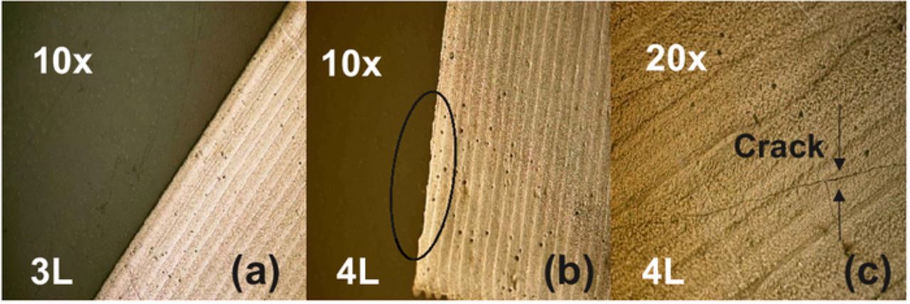
Figure 5. Microscopic image (10x magnification) of edge of 3L and 4L printed samples sintered at 120°C (a) even edge at 3L printed pattern (b) uneven edge at 4L printed pattern (c) crack formation at 4L printed pattern.
The mechanical stability of the inkjet printed three-layer pattern was tested using repetitive bending and adhesion test. Tensile bending was used as studies indicate it had a more detrimental effect on the printed pattern than compressive bending.18 Two cylindrical shapes of diameter 14 mm and 30 mm were selected. It was found that the printed patterns were flexible around the cylinder without any crack or deformations (Figure 6). On the other hand, adhesion of the ink to the substrate was measured using ASTM tape test. The PET surface was inspected after the tape pull off using the microscope (Figure 7).
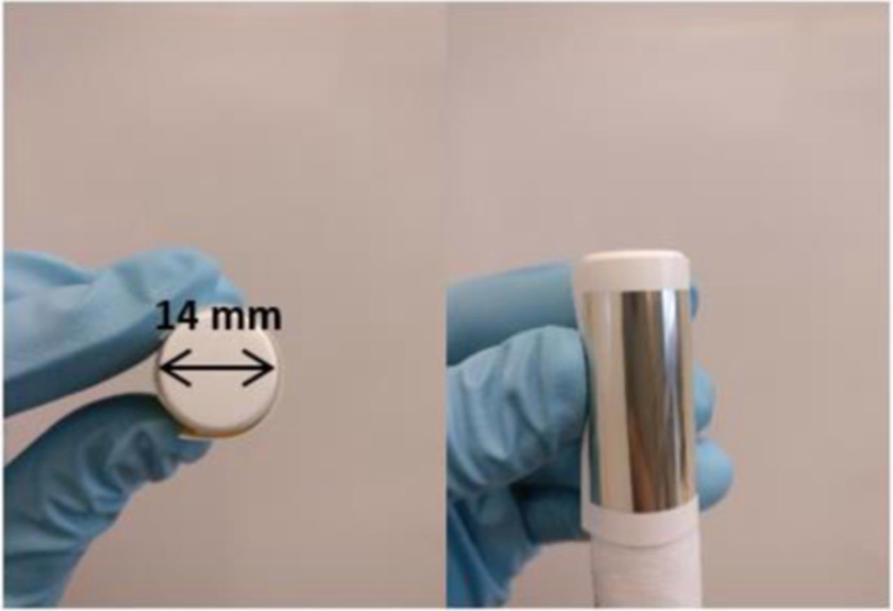
Figure 6. Repetitive bending test of printed samples.
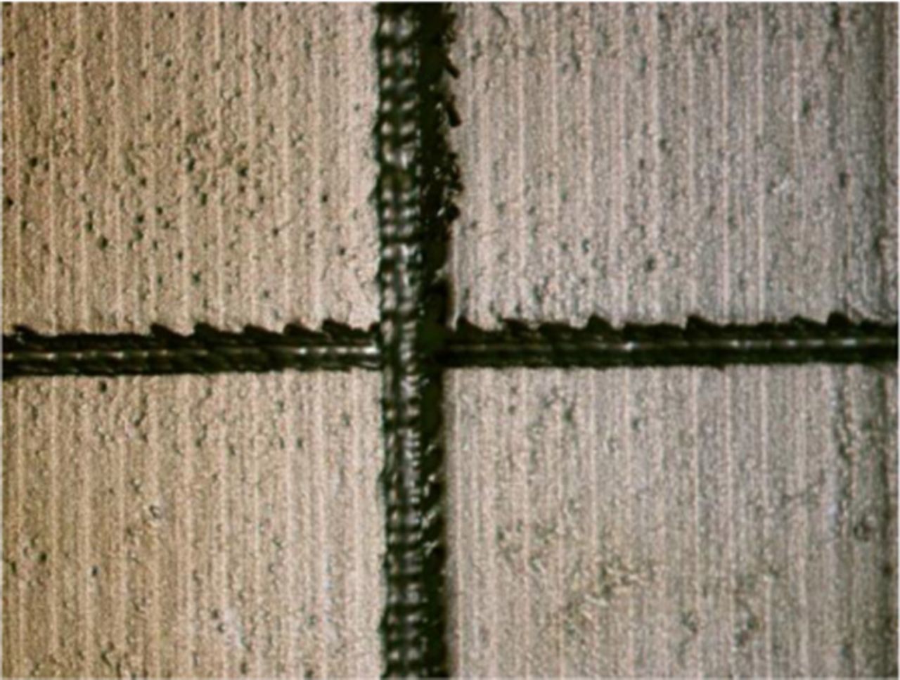
Figure 7. CD Microscopic image after tape pull off in ASTM tape test.
The edges of the cut were found smooth with nominal ink detachments. The adhesion rating was found to be class 4B indicating less than 5% of the test area is detached due to tape pull off. The bending and adhesion tests indicate a mechanically stable pattern on the PET surface.
Conclusions
In summary, the impact of drop spacing, printing layers, and sintering temperature were investigated to fabricate highly conductive and flexible inkjet printed samples on PET. It was observed that a drop spacing of 20 μm provided good printing performance. The sintering temperature and the number of printing layers were found to be statistically significant factors influencing the electrical conductivity. The highest conductivity was found in samples with three layers of printing and subsequent post heat-treatment of 120°C. Further increase in printing layers generated crack because of non-uniform heat conduction in the thick Ag layer. The three-layer printed samples were found to be mechanically stable without any conductivity based on ASTM tape test and bending test. The optimized printing parameters on PET substrate can lead to inexpensive electronic devices for Internet of Things (IoT) applications.
ORCID
Praveen Kumar Sekhar 0000-0002-4669-535X