Abstract
A novel experimental technique for making electrochemical measurements on individual phase or isolated regions of a metal or alloy is reported. The technique, called Selective Masking by Photolithography (SMP), uses a hardened photoresist coating to mask the excluded portions of the sample and 355 nm laser pulses are employed to expose individual grains or regions of interest. The size of the exposed area can range from tens of microns to millimeters. Localized electrochemical DC and AC measurements and critical pitting temperature determinations for the two phases in a duplex stainless steel were used to show the utility and viability of SMP.
Export citation and abstract BibTeX RIS
One of the challenges associated with electrochemical testing is that it is difficult to determine individual contributions to a measured current especially when the sample area comprises multiple grains, grain boundaries, precipitates, etc. The heterogeneity of such areas result in competing kinetic processes that contribute to the overall current. For studies that are aimed at determination for example, of corrosion resistance or catalytic activity, it would be beneficial to have a versatile technique that can isolate areas of interest. Localized experimental procedures using micro-capillaries1–3 to probe small areas of the sample surfaces have been developed previously. Though the micro-capillary technique has been in widespread use for the past 15 years, aspects of the technique make it undesirable for certain experimental procedures. For example, the relatively fast potentiodynamic sweep rates required to prevent cell leakage or tip blockage of the micro-capillary prevent scanning at rates as slow as 10 mV/min and the micro-capillary tip diameter can affect the limiting current passing through the cell.4 In addition a flat, polished surface is need for this technique.
This communication describes and demonstrates the utility and viability of a novel experimental technique, Selective Masking by Photolithography (SMP), for making electrochemical measurements on individual phase or isolated regions of an alloy. In this work, the technique was used to isolate individual ferrite and austenite phases from their neighbors on a polished duplex stainless steel sample (alloy 2205). Alloy 2205, UNS S32205, is a corrosion resistant alloy that consists of approximately equal amounts of δ-ferrite and γ-austenite phases. Polarization scans, electrochemical impedance, and critical pitting temperature experiments were then performed on these isolated regions. In this work, the sample surfaces were flat and polished but the technique could be used to study irregular surfaces. Although the application for this work is related to corrosion, SMP has wide applicability to any electrochemical study that explores the behavior of individual phase or isolated regions of interest.
Experimental
Sample preparation and phase selection
Duplex stainless-steel 2205 cast samples were provided by Wärtsilä (Chesapeake, VA). The phase compositions were determined via the energy dispersive x-ray spectroscopy (EDS) probe on a LEO 1550 Scanning Electron Microscope (SEM). The measured compositions are shown in Table 1.
Table I. Composition (atomic%) of the δ and γ phases in the 2205 samples – as determined using EDS.
| Phase | Fe | Cr | Ni | Mo | Mn | Si | C |
|---|---|---|---|---|---|---|---|
| γ - Austenite | 66.48 | 22.16 | 6.71 | 1.43 | 1.24 | 1.98 | 0.18 |
| δ - Ferrite | 63.95 | 23.89 | 4.38 | 3.83 | 0.84 | 1.12 | 0.18 |
The samples were machined to 19 mm × 19 mm × 2 mm coupons and polished by hand through 1200 grit sandpaper then mechanically polished using 0.05 micron alumina for up to 18 hours on a vibratory polisher. A 10 × 10 square grid composed of 1 mm squares was laser machined onto the surface using a pulsed ultraviolet laser in order to provide reference marks for locating regions of interest to be tested. The reference markings are shown in Figure 1.
Figure 1. Secondary electron image of the laser machined gridlines showing the depth of the machined lines with minimal impact to the surrounding region. The grid squares are labeled in the lowest left corner as rows A–J and columns 0–9.
The first step in the process for performing electrochemical measurements of specific phase regions required identifying the different phases and regions of interest on the surface of the sample. Optical microscopy provided sufficient contrast between the austenite phase and ferrite matrix on the surface and therefore was used for much of the initial screening of the 2205 samples – as seen in Figure 2. However, in cases in which the crystalline orientation needed to be known, the screening process was done from crystalline orientation maps obtained from electron backscatter diffraction (EBSD) scans.
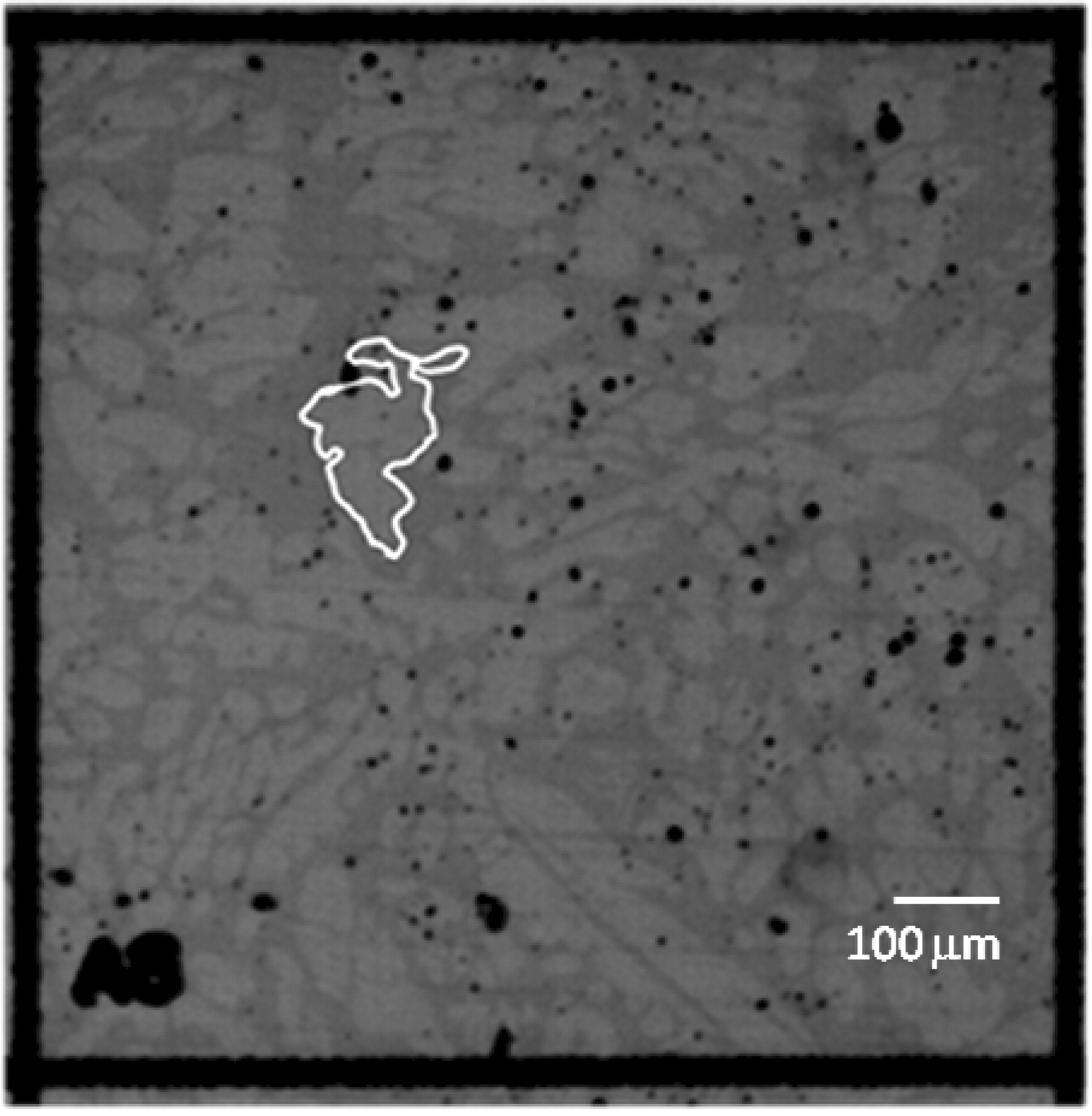
Figure 2. Optical microscopy image of an austenite region of interest that will be uncovered via ultraviolet exposure of the insulating photoresist.
The second step in the procedure was the isolation of these selected phase regions using the SMP technique. This technique is based on laser lithography – a well-established direct-patterning technique that avoids the complexity and cost of mask fabrication. An UV (355 nm) solid state (Nd:YVO4) laser (Spectra-Physics YHP40) with maximum pulse energies of ∼300 μJ and pulsewidths of ∼30 ns (FWHM) was used as the laser source and details of the laser/motion-control system are provided elsewhere.5 A 1 μm-thick layer of Microposit S1818 photoresist was spin-coated onto the sample surface and soft-baked at 110°C for 1-2 min on a hot plate. The areas of interest were then mapped by translating the sample on a high-resolution (10 nm) X-Y stage as it was exposed to individual 355 nm laser pulses that were focused through a 20X microscope objective into approximately 40 μm diameter spots on the sample surface. The energy of the laser spot was measured to be ∼2.6 μJ corresponding to a fluence of ∼200 mJ/cm2 on the surface, which did not damage the steel, but was sufficient to expose the photoresist. After exposure, the sample was immersed in a developer solution (Microposit MF-319) which removed the photoresist coating to reveal the bare steel surface of these selected regions while the rest of the surface was still protected by the unexposed photoresist. The sample was then hard-baked at 150°C for 60 minutes to improve the coating reliability and adhesion during corrosion testing. Multiple 'windows' were opened on the surface coating and were robust enough to allow several corrosion experiments to be performed on the same sample. Figure 3 illustrates the laser lithography process on the sample.
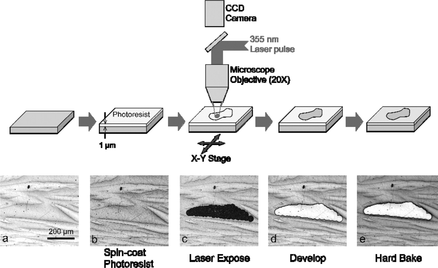
Figure 3. Schematic diagram of the procedure used to expose and isolate individual phases and the corresponding images of each step for a ferrite region of a 2205 steel sample. A green (UV blocking) filter is used in b) and c) to prevent light emission from the microscope illuminator from further exposing the photoresist.
Electrochemical measurements
Each photoresist-coated sample had multiple windows emplaced over various phase regions, so a procedure was developed to electrically isolate the sample and the other windows so that only a single phase region or boundary was exposed to the electrolyte. A small hole-punch (approximately 3 mm in diameter) was used to create a window in the Kapton polymide tape that would isolate the window of interest from the surrounding grids. Kapton polymide tape was chosen because its adhesive properties did not damage the photoresist coating between repeated application and removal. A zip-lip, 2"× 3", 2 mil thick polyethylene bag was used to provide electrical isolation from the electrolyte. A hole was cut into the bag using a brass cutter that was larger than the Kapton tape window and the edges of the hole were sealed using Scotch Brand 1280 EMP electroplater's tape. Figure 4 illustrates the results of this process.
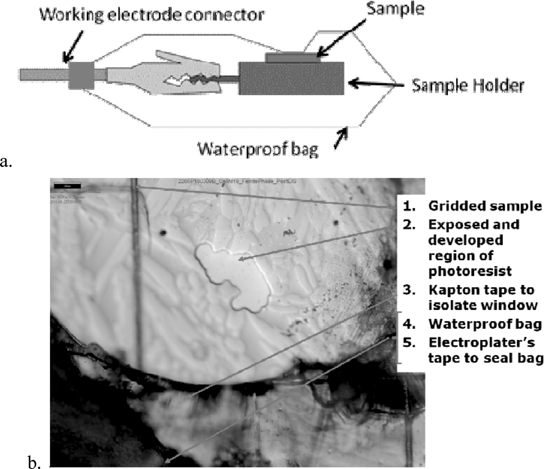
Figure 4. a. Schematic diagram showing the set-up for providing a conducting path for the electrons to and from the active surface and how the set-up was electrically shielded from the electrolyte. b. Optical microscopy image showing the layers of waterproof material used to electrically isolate a specific window in order to ensure only the properties of the phase type of interest were measured.
Seawater source for this work was the U. S. Naval Research Laboratory (NRL) in Key West, FL. The coastal waters surrounding Key West, FL tend to be oligotrophic and fairly representative of open-ocean or "blue" water, which imparts a high degree of consistency annually. The properties of the seawater used for this testing were 35.5 PSU salinity and 8.03 pH. The seawater was pasteurized at 65°C for a minimum of 12 hours prior to use. Polarization scans that were performed in a deaerated environment were obtained by bubbling argon gas into the sealed cell.
Results
Experimental approach
The experiments were divided into two sets. The first set consisted of proof-of-concept tests to determine the procedure that would be followed and to establish baseline measurements of the properties of the material. The second set of experiments was designed to explore the effect of temperature on pitting corrosion in austenite and ferrite and to measure the characteristics of the oxide films that formed over the austenite and ferrite using electrochemical impedance spectroscopy.
Baseline measurements
For comparison to the individual grain experiments and to test the preparation procedure for a 0.005 cm2 portion of one of the grid cells was exposed by the laser and tested in aerated seawater. The resulting polarization curve is shown in Figure 5. The current density from the exposed region ranged from 10−7 to ∼10−6 A/cm2 as the potential was increased from −0.5 to 1.0 VSCE. Two other samples were selectively etched using a combination of aggressive solution chemistries and potentiostatic holds at potentials that corresponded to the active corrosion peaks for each phase.9 This selective etching process removed either the ferrite or austenite grains depending on the potential. These samples were then coated with the photoresist and lightly polished using 600 grit silicon carbide to remove the photoresist from the unetched phase. Thus the electrochemical behavior of a high surface area of either the austenite or ferrite could be obtained and compared to the response from samples prepared using SMP. These bulk exposed ferrite and austenite samples were also tested in aerated seawater and the results illustrated in Figure 5.
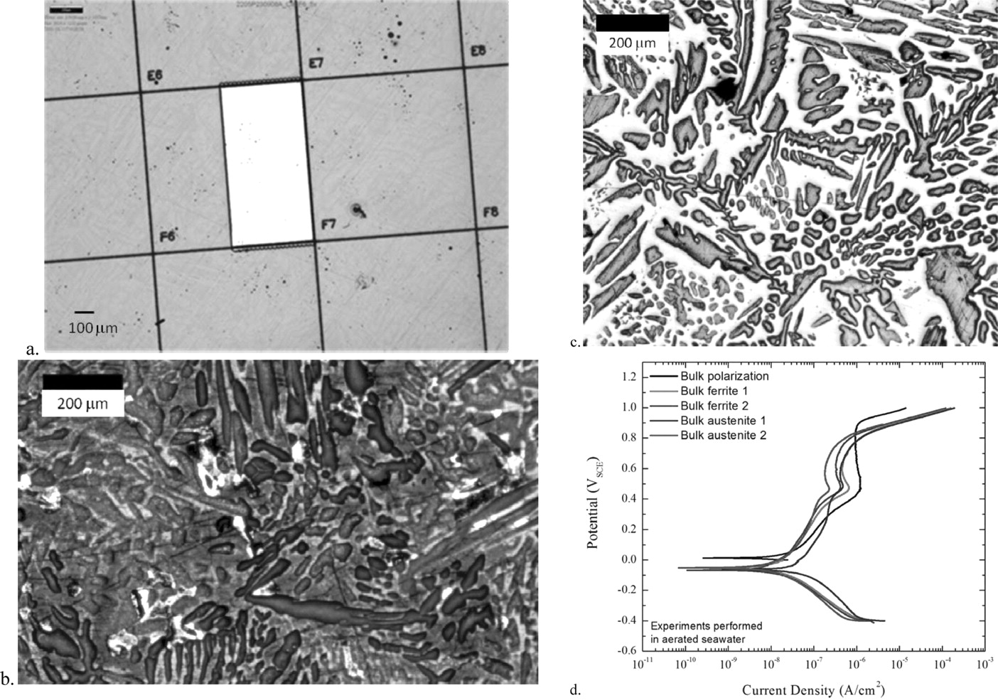
Figure 5. a. Optical microscopy image of the 1 mm x 0.5 mm window used for the bulk polarization scan. b. Optical microscopy image of the ferrite-etched, austenite-exposed sample. c. Optical microscopy image of the austenite-etched, ferrite-exposed sample. d. Polarization scans of the bulk exposed regions and the ferrite and austenite etched regions in seawater with ambient aeration.
Solution resistance and impedance measurements
As detailed in the following section, making electrochemical measurements on such small areas of exposed metal presented several challenges to ensure that valid measurements were being obtained. For example, one of our concerns was that solution resistance, due to current crowding in the vicinity of the exposed region of the photoresist, would affect measurements. To evaluate the magnitudes of the solution and polarization resistances, we performed impedance measurements on exposed austenite and ferrite regions that had been held at their open-circuit potential for two hours in aerated seawater.
The solution resistance between the exposed region and the reference electrode for samples with areas on the order of 10−4 cm2 was measured to be 515 Ω = 0.206 Ω ·cm2 from the Nyquist plots shown in Figure 6a. Figure 6b shows an adjusted polarization scan showing the corrected potential applied to the interface as compared to the measured values. The similarity between the two plots indicates that the ohmic IR drop between the sample and the reference electrode is negligible in polarization scans done on the regions exposed by the micro-windows. The polarization resistances varied widely for both austenite and ferrite and independently of the exposed area. Additional measurements are necessary to determine if there are differences due to crystalline orientation but these experiments demonstrated ability to make the electrochemical measurement on SMP samples.
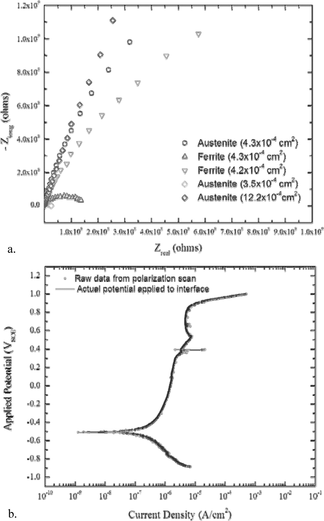
Figure 6. a. Nyquist plots for austenite and ferrite regions of various areas exposed to aerated seawater. b. Comparison between the measured polarization scan (open-circles) and the solution resistance corrected scan (solid line) showing virtually no difference because the solution resistance was small compared to the polarization resistance.
Effect of the size of the exposed area on the current measurements
The area exposed on the sample following development of the photoresist was determined using a numerical integration algorithm in the Alicona Infinite Focus Microscope image analysis routine. Figure 7 illustrates the result.
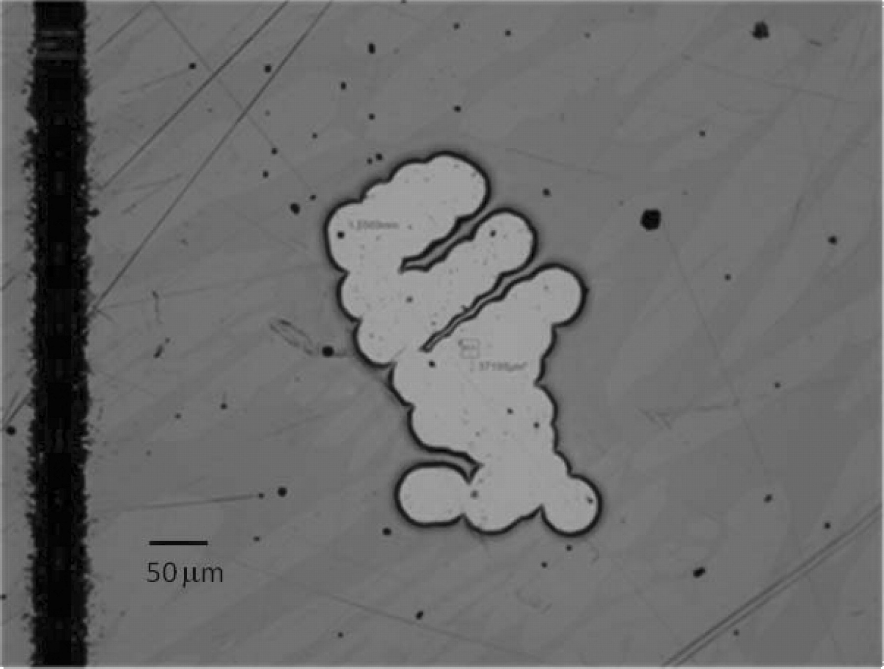
Figure 7. Optical microscopy image with image analysis overlay showing the polygon outline used to determine the exposed metal area. In this case, the exposed area of the austenite phase was ≈3.72 × 10⁻⁴ cm2.
For measurements conducted using a Gamry Series G 750 potentiostat, which can detect changes as small as 0.01 pA and has a leakage current of around 5 pA, the experimental set-up had a low-current limit of approximately 100 pA - regardless of the type of exposed phase. This translated into an exposed-area limit of no less than 3.0 × 10⁻⁴ cm2. For measurements conducted using a Gamry Reference 600 potentiostat, with its correspondingly better sensitivity, the practical exposed area limit was roughly 1.0 × 10⁻⁴ cm2.
Figure 8 illustrates how, once the size of the exposed area decreased, the potentiostat began to be affected by the ambient electromagnetic noise in the room and was eventually unable to resolve the corrosion current throughout the entire polarization scan, thus setting the lowest limit of exposed area for making measurements.
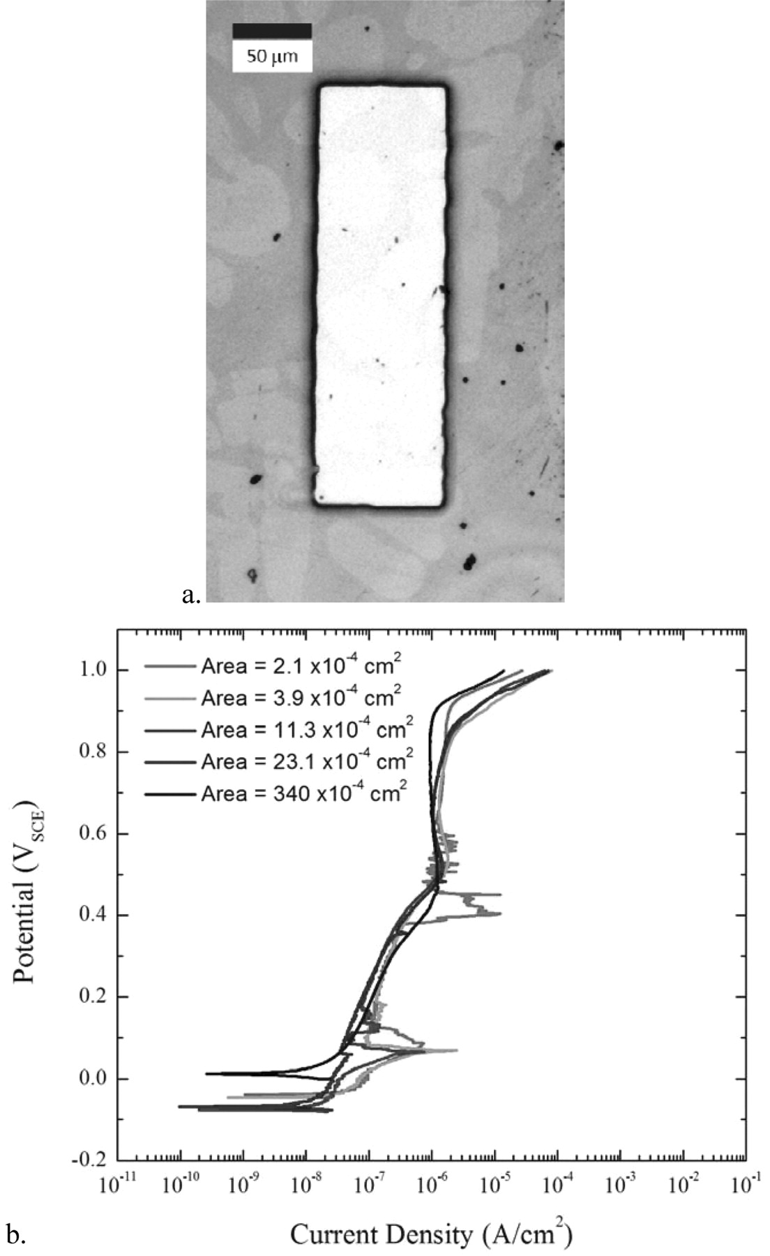
Figure 8. a. Optical microscopy image of the smallest exposed rectangular area of 2.1 × 10⁻⁴ cm2. b. Plot of the polarization scans taken in aerated seawater of progressively smaller exposed areas showing that, even though the current density remained consistent, as the exposed area decreased, the noise in the current measured by the potentiostat increased as the total corrosion current decreased.
Austenite phase results
In order to perform DC electrochemical experiments on individual phases of known crystalline orientation, we mapped cells in the surface grid using the EBSD camera to obtain the orientations of the various phases and identify the grains to be tested. The phase regions that had similar orientations within a cell were then laser processed and developed prior to undergoing a polarization scan in deaerated seawater. The polarization scan from a test on a single region of the austenite phase with a (111) orientation is shown in Figure 9. Polarization scans from a selection of austenite phase regions with their respective crystalline orientations are shown in Figure 10.
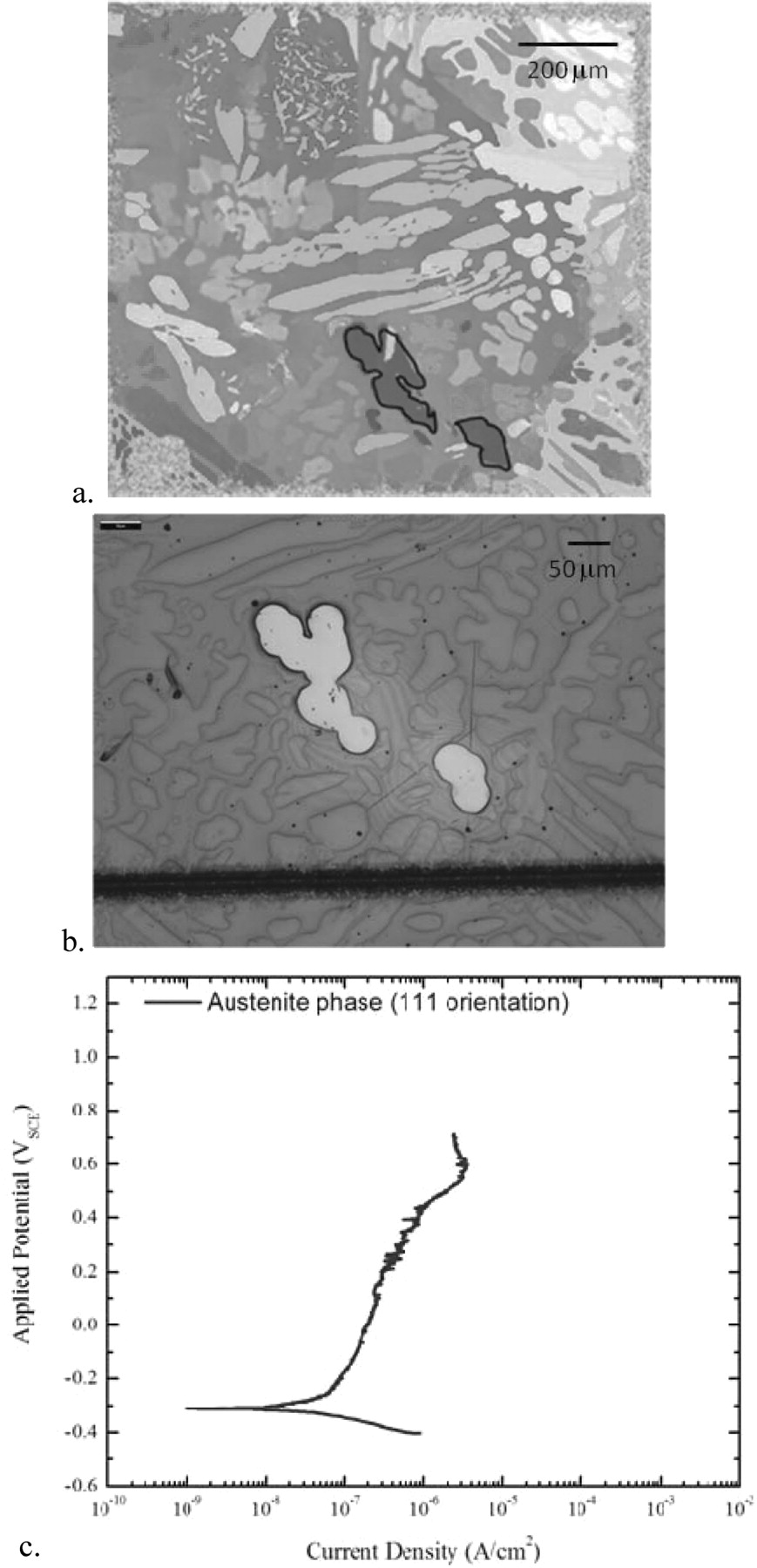
Figure 9. a. EBSD image of cell A0 with the (111) austenite phase region of interest highlighted with a dark line. b. Optical microscopy image of the window over the austenite region in Cell A0 shown above. c. Polarization scan for the austenite phase exposed to seawater and deaerated in Ar.
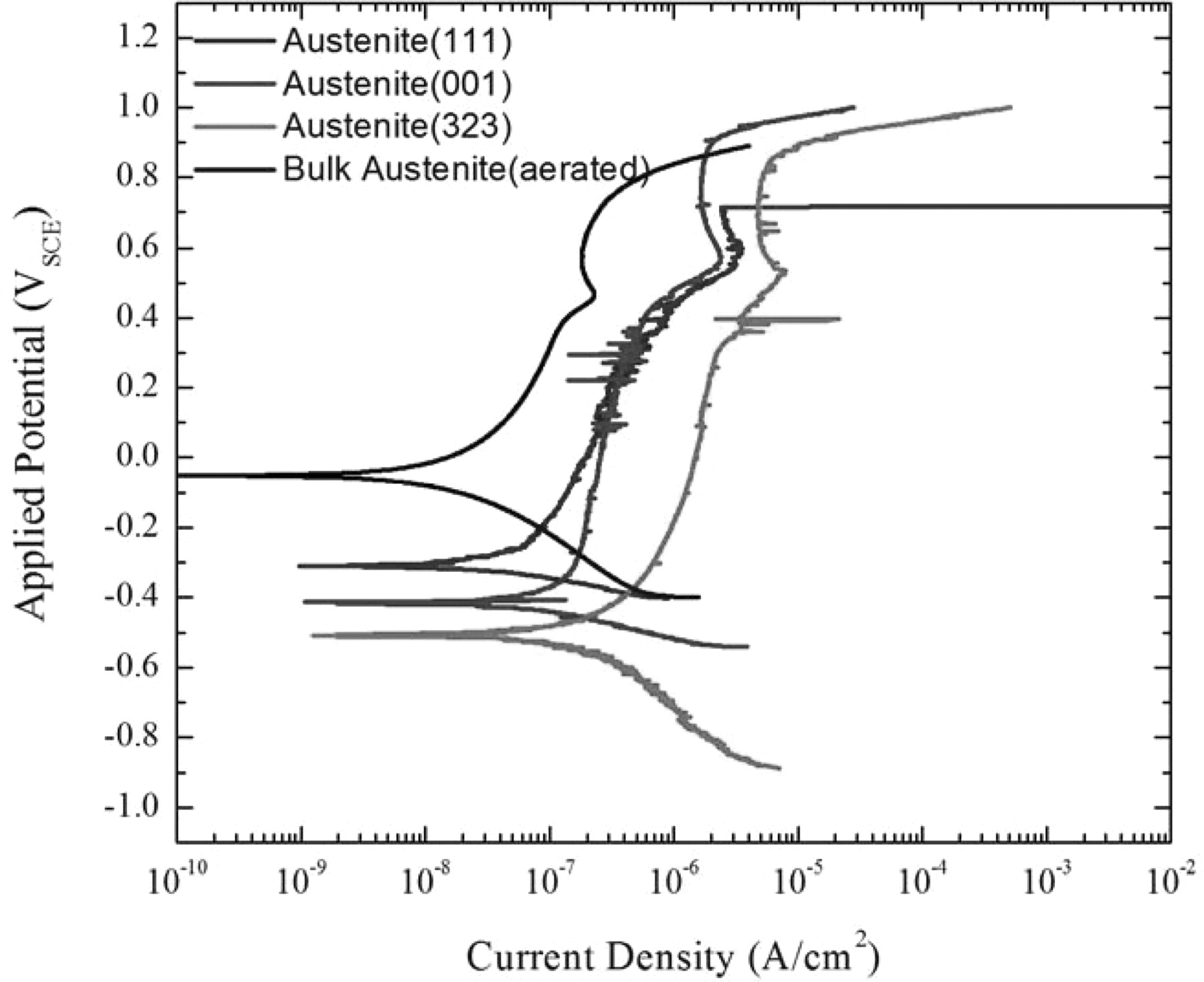
Figure 10. Polarization scans of austenite phases exposed to seawater and deaerated with Ar. The polarization scan for the bulk austenite in aerated seawater is shown for comparison.
Ferrite phase results
The polarization scan from a test on a single region of the ferrite phase with a (203) orientation in deaerated seawater is shown in Figure 11. Polarization scans from a selection of ferrite phase regions with their respective crystalline orientations are shown in Figure 12.
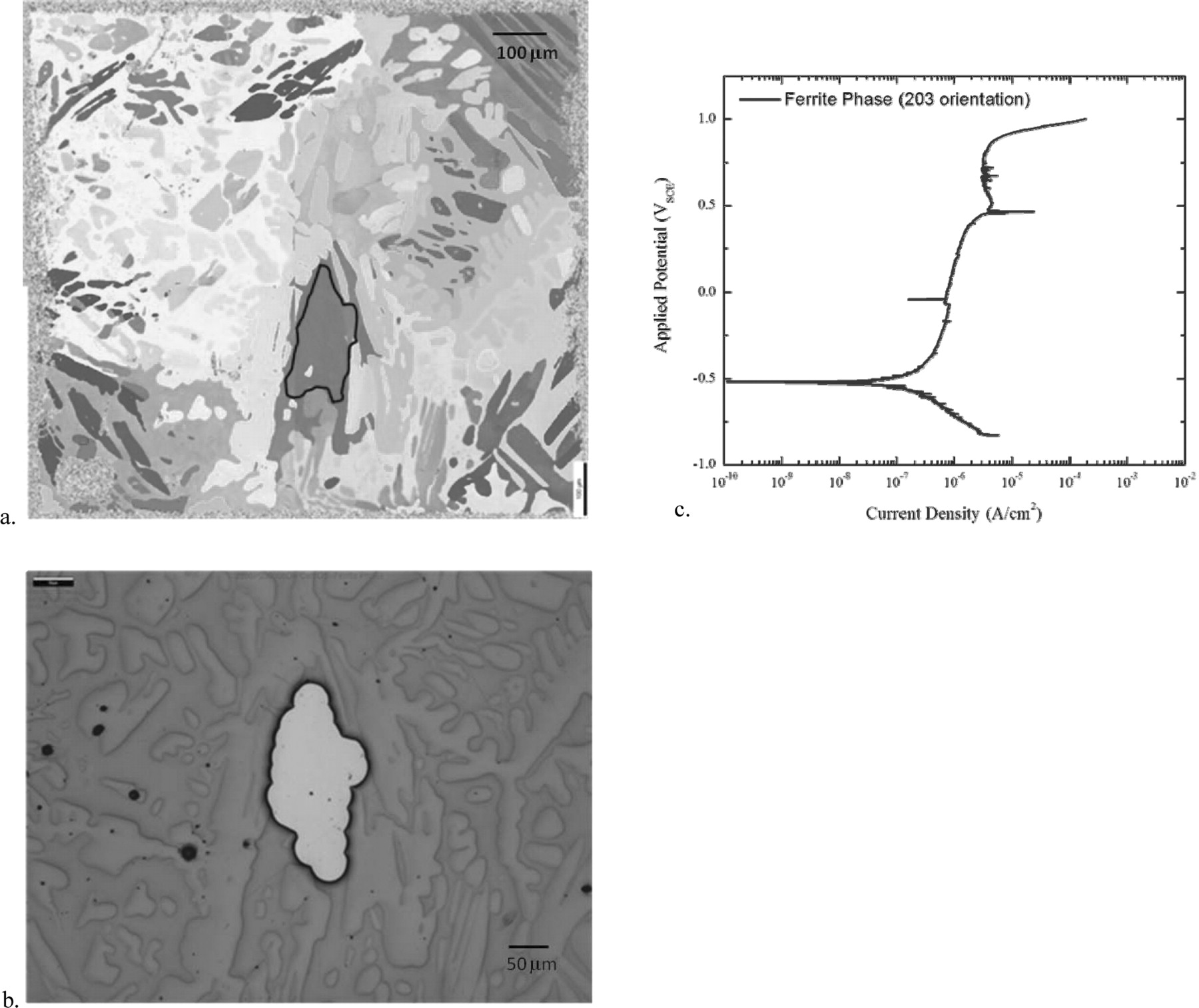
Figure 11. a. EBSD image of cell G9 with the (203) ferrite phase region of interest highlighted with a dark line. b. Optical microscopy image of a window over a region of the ferrite matrix in Cell G9. c. Polarization scan of the ferrite phase exposed to seawater and deaerated in Ar.
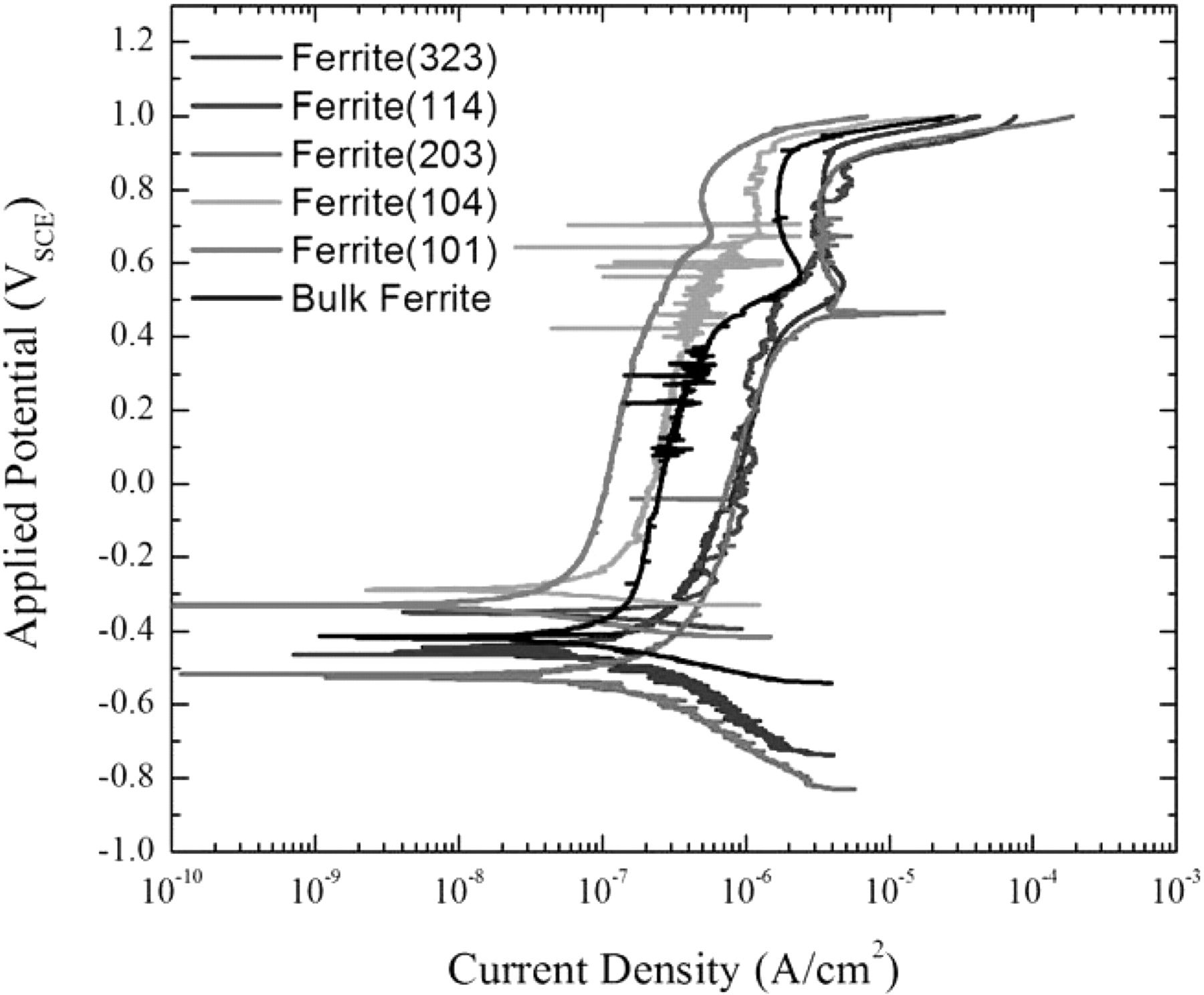
Figure 12. Polarization scans of ferrite phases exposed to seawater and deaerated with Ar. The polarization scan for the bulk ferrite in aerated seawater is shown for comparison.
Electrochemical impedance spectroscopy
In this section, the impedance behavior of the ferrite and austenite phases in seawater is presented in contrast to the behavior of the bulk alloy in seawater. The impedance tests were carried out in 50 mV increments from −400 mVSCE to + 1000 mVSCE. The AC potentials were ±10 mV RMS and the frequencies ranged from 1 × 10⁵ to 1 × 10⁻² Hz at each potential. Nyquist plots for austenite, ferrite, and the bulk alloy at 5 different potentials are shown in Figure 13.
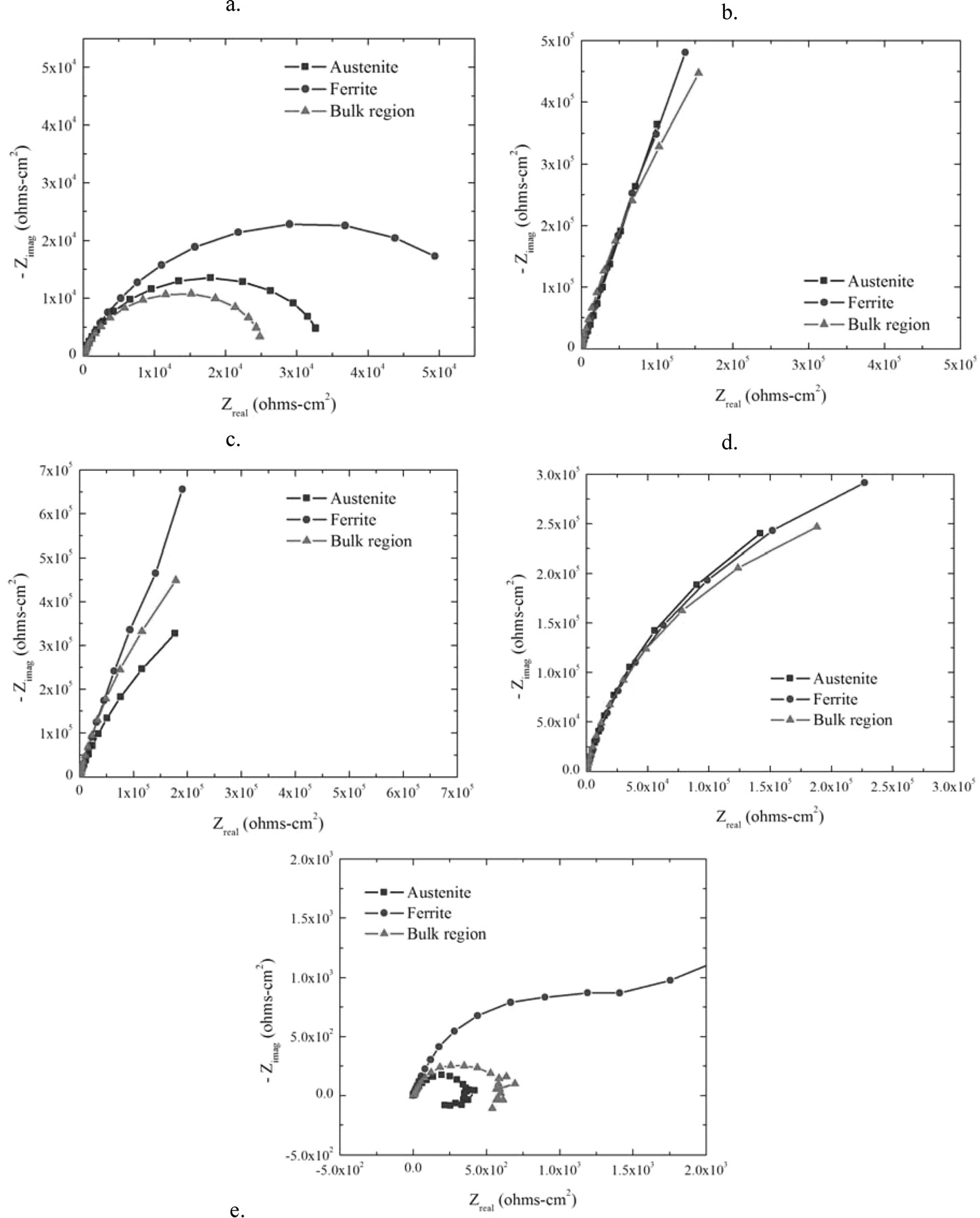
Figure 13. Nyquist plots for austenite, ferrite, and the bulk alloy at a) −400 mV, b) 0, c) +400 mV, d) +800 mV, and e) +1000 mV.
Assuming that the oxide film impedance can be modeled using a solution resistance in series with a parallel circuit of a polarization resistance and constant phase element – as shown in Figure 14 – then the depth of the electrically active region of the oxide film can be determined using Equation 1.
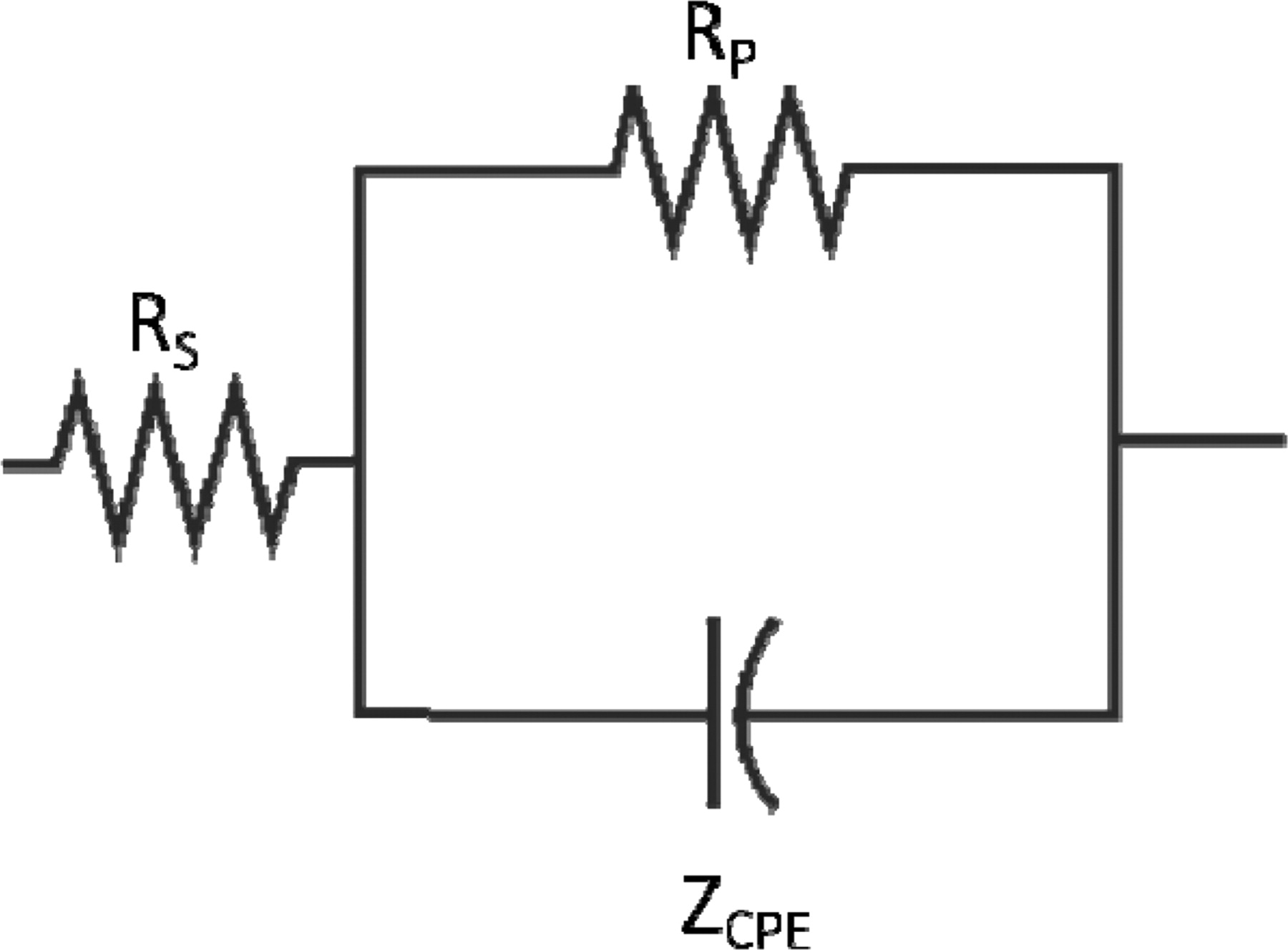
Figure 14. Equivalent circuit model of the metal-electrolyte interface where RS is the solution resistance, RP is the polarization of the interface, and ZCPE is the impedance of the constant phase element.
where Cdl is the double-layer capacitance, ɛ0 is the free-space permittivity = 8.85 × 10⁻¹⁴ F/cm, ɛ is the dielectric constant for the oxide film – assumed to be about 15.6,8 A is the exposed area, and L is the depth of the active region of the oxide film.
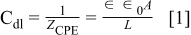
The measured currents of the polarization curves – shown in Figure 15 – suggest that at potentials below −400 mVSCE, the oxide film is removed from the surface by the cathodic polarization but above −400 mVSCE to about + 200 mVSCE, the film covers the active surface and begins to thicken. Above +200 mVSCE, even though the surface is still passive, the electro-active region of the film decreases, suggesting that the film is thinning or depleting a more active metal ion from the film. Above +400 mVSCE, it appears as if another anodic reaction begins to dominate the dissolution process, but above +850 mVSCE, that reaction is exhausted. Above +950 mVSCE, the current rapidly begins rising as oxygen evolution begins and the oxide film is dissolving as quickly as it is formed.
Figure 15. a. Plots of the depth of the electro-active region of the oxide film for two bulk areas of the sample surface. b. Optical microscopy image of a bulk area exposed for testing. c. Plots of the depth of the electro-active region of the oxide film for two austenite areas of the sample surface compared against a bulk region. d. Optical microscopy image of an austenite area exposed for testing. e. Plots of the depth of the electro-active region of the oxide film for two ferrite areas of the sample surface compared against a bulk region. f. Optical microscopy image of a ferrite area exposed for testing.
Critical Pitting Temperature
At room temperature in seawater, neither austenite nor ferrite in 2205 is susceptible to pitting. The phases in these samples had estimated Pitting Resistance Equivalent Numbers (PREN) of 30.4 for the austenite and 36.16 for the ferrite. However, as the temperature of the seawater bath was elevated, metastable pitting events were observed above 45°C with pitting occurring in ferrite around 61°C and in austenite around 63°C – as shown in Figure 16. There were limited repetitions so additional experiments would need to be performed before assigning statistical significance to the results, but these tests do show that SMP can be used to make Critical Pitting Temperature measurements.
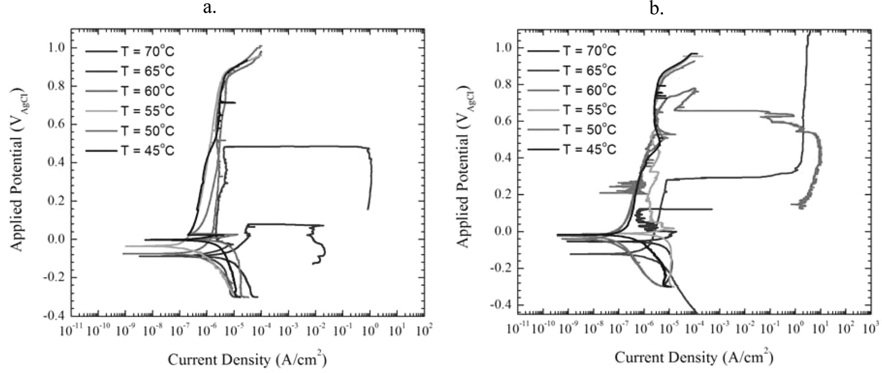
Figure 16. a. Plots of polarization curves for regions of austenite exposed to seawater at temperatures from 45°C to 70°C in 5 degree increments. b. Plots of polarization curves for regions of ferrite exposed to seawater at temperatures from 45°C to 70°C in 5 degree increments.
Discussion
Using the SMP technique to mask off the untested areas of the 2205 samples allowed polarization scans to be performed at slow scan rates and without the concern of corrosion products obstructing the current path. The high oven temperature and long, ∼60 minute baking times for the photoresist inhibited the development of crevice corrosion under the photoresist at the edges of the exposed regions, as shown in Figure 17.
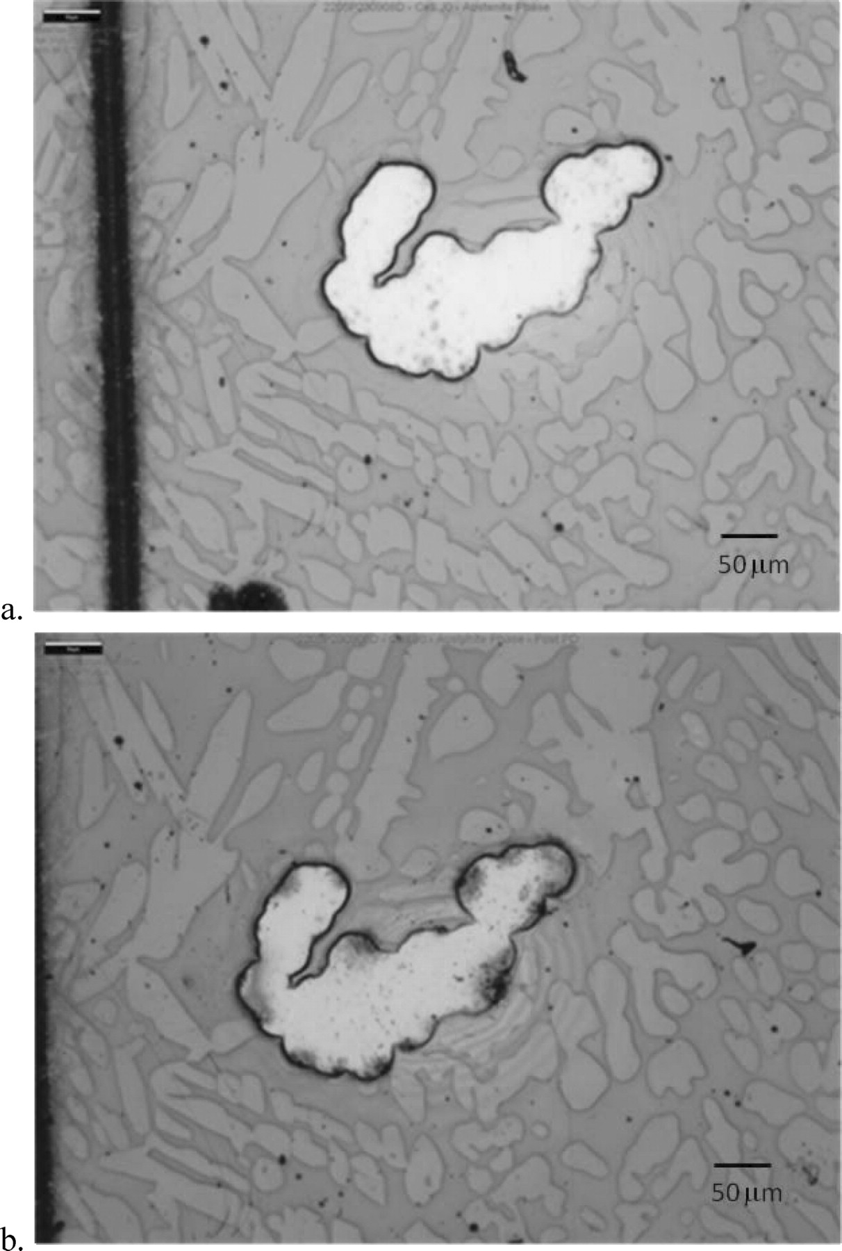
Figure 17. a. Optical microscopy image of an exposed austenite phase region prior to a polarization scan. b. Optical microscopy image of an exposed austenite phase region after a polarization scan. The dark regions on the borders do not show other evidence of under-cutting of the photoresist that would be expected in crevice corrosion.
The corrosion current was directly related to the dimensions of the exposed area of the sample so that it was possible to expose and develop an area that had a corrosion current that was too low to be measured by the available potentiostats. Polarization resistance dominated the current path with values range from 106 ohms to 109 ohms, with the solution resistance a manageable value of a few hundred ohms, as compared to solution resistances on the order of 103 ohms for a microcapillary of similar dimensions.4,6 The relatively low solution resistance allowed us to perform impedance measurements on the individual phases.
Alloy 2205 is a passive alloy that does not pit at room temperature in seawater but its oxide film does break down at very anodic potentials. Both phases exhibited a passive current density on the order of 10−6 A/cm2 under anodic polarization between the open-circuit potential and a secondary dissolution peak around +0.5 VSCE, followed by another region of passivity above the secondary dissolution peak before evolving oxygen. However, as was shown above, as the temperature of the sample was increased, stable pitting was observed in both phases. Figure 18 plots the potential at which the corrosion current density exceeded 10−4 A/cm2 versus temperature for each phase and shows that ferrite and austenite behave quite differently at temperatures between 60°C and 65°C. This is consistent with the observations of by Moayed and Newman7 showing that metastable pitting is different in austenite and ferrite and further demonstrates the ability to use SMP to obtain information on specific grains.
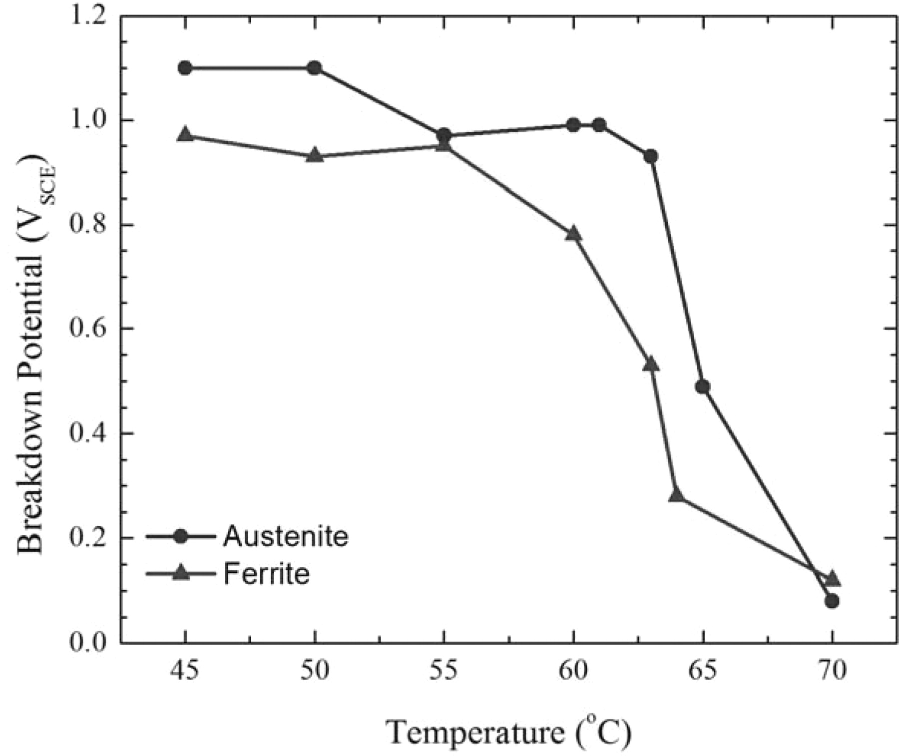
Figure 18. Plot of the breakdown potential as a function of temperature for austenite and ferrite showing a difference in behavior between 60°C and 65°C where the transition to stable pitting occurs.
Results obtained from using the SMP technique suggest there are differences in the behavior of the passive films as a function of potential and temperature, indicating that phase composition plays a role in the corrosion resistance of the alloy. The next step in the process is to investigate differences in corrosion behavior due to crystalline orientation and phase. An initial example, polarization curves for austenite and ferrite with similar crystalline orientations, is shown in Figure 19.
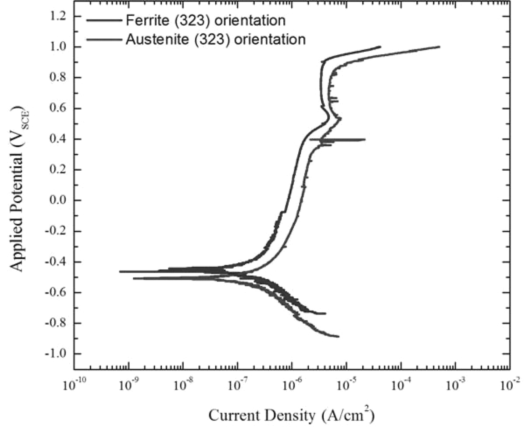
Figure 19. Comparison of the polarization scans between austenite and ferrite of similar crystalline orientation in deaerated seawater.
Conclusions
The results obtained from using the SMP technique demonstrate that it can be used to perform DC and AC electrochemical experiments on surface regions with an exposed area of < 10−4 cm2 – including irregularly-shaped regions such as cross-sectional areas of the dendrite fingers of the austenite phase in the 2205 duplex stainless steel. It is important to note that the area that can be interrogated is related to the current sensitivity of the potentiostat. Although the application for the present work is related to corrosion, SMP has wide applicability to any electrochemical study that explores the behavior of individual phase or isolated regions of interest.
Using SMP, differences in the impedance behavior of the oxide films and the transition to stable pitting above the critical pitting temperature have been investigated for ferrite and austenite regions in a duplex stainless steel. The results also indicate crystalline orientation does not appear to play a role in the passive current density. However, a larger sample population of the different crystalline orientations in each phase needs to be tested to be able to draw statistically significant conclusions.
Acknowledgments
The authors gratefully acknowledge the financial support of the Naval Research Laboratory and the Office of Naval Research.