Abstract
The need for low-cost and highly versatile photosensing devices keeps increasing. In this work, we present a heterojunction device based on wafer-scale graphene grown by chemical vapor deposition (CVD) and sputtered InGaZnO (IGZO) semiconductor for dual mode photocurrent collection. The photocurrent can be collected either from the lateral gold/graphene/gold configuration or from the vertical graphene/IGZO/nickel heterojunction configuration with no external bias. Incident-energy-dependent photocurrent scanning microscopy shows that the dominant photocarriers are formed at the edge of the gold electrode through photo-thermoelectric hot hole generation in the lateral configuration. Vertical mode renders unidirectional current flow by photoexcited electrons in the IGZO and the subsequent relaxation and diffusion due to Fowler-Nordheim potential.
Export citation and abstract BibTeX RIS
Graphene is a two dimensional carbon-chained material that has been extensively studied for promising photonic and optoelectronic applications.1–3 Zero bandgap and a fast carrier relaxation process in intrinsic graphene facilitate ultra-broadband and ultrafast light detectors.4–7 Under light illumination, graphene with lateral contact electrodes generates photocurrent through a photovoltaic, bolometric, or photo-thermoelectric mechanisms depending on bias and gating conditions.8–15 Recently, photodetectors based on graphene heterojunctions have been extensively highlighted. Currently, Schottky-barrier-type vertical heterojunctions composed of graphene/silicon,16–20 reduced-graphene-oxide (RGO)/silicon,21 and RGO/silicon nanowire22 have been successfully demonstrated. Unlike lateral photocurrent collection, the vertical junctions take advantage of an asymmetric barrier potential to efficiently separate photoexcited electrons and holes, which might pave the way for light detection with large active areas without the need for external source-drain bias.
Here, we demonstrate a heterojunction device capable of dual mode photocurrent collection under zero source-drain bias based on a graphene grown by chemical vapor deposition (CVD) and amorphous-phase indium gallium zinc oxide (IGZO). Here, dual mode means that the photocurrent can flow either from a lateral pair of the electrodes or from a vertical pair of electrodes. Versatile photodetection schemes allow to broaden the range of selection for applications such as photo-energy harvesting, phototransistor, and photoconductive detector.1,2,14 Unlike silicon, IGZO semiconductors can be grown on glass substrates at low temperatures, typically below 200°C so that large area device fabrication is possible. IGZO has been widely used for image sensors, flat-panel displays, and thin film transistors.23–25 The typical mobility of the IGZO film is about 10–60 cm2/Vs.23,25,26 Interestingly, the graphene/IGZO junction is known for triangular Fowler-Nordheim potential showing no pinned interface potential.27 As a result, low bias field-effect transistor operation is possible in the vertical configuration where the tunneling probability is given by  .27,28 Here, m*, e, ħ, ε , and ΔWM are the effective mass of an electron in the barrier, the electric charge, the reduced Planck constant, the electric field across the barrier, and the barrier height, respectively. Therefore, unidirectional photocurrent may be generated in the vertical mode without applying external bias under appropriate illumination condition.
We investigate excited carrier types and transport mechanisms under laser illumination by incident-energy-dependent photocurrent scanning microscopy. The photodetection performance, estimated by photoresponsivity, is usually presented in the literature when the highest value is obtained under large source-drain bias or gate bias. However, source-drain or gate bias induces large dark current that is not favorable for energy efficient photodetection. Also showing responsivity values under large bias hinders fair comparison of performance and mechanism under low field operation from device to device. In this work, we investigate photoresponsivity, temporal response, and scanning micrographs with no external bias. In the vertical mode, electrons excited in the IGZO layer are found to be majority carriers. The photoexcited electrons quickly relax in the IGZO layer and diffuse owing to Fowler-Nordheim potential formed at the IGZO layer. As a result, the photocurrent direction is found to be opposite to the case of the previously-reported Schottky junctions.17 For the case of lateral mode, antisymmetric photocurrent was measured owing to surface-plasmon-mediated hot carriers generated in the gold electrodes. Comparing the incident-energy-dependence with recently reported first-principle calculations provides a reasonable explanation for the origin of the photocarriers in the lateral mode.
Experimental
Graphene/IGZO heterojunction devices were fabricated on a 700-μm-thick six-inch glass wafer with a 450-Å-thick nickel layer as the bottom electrode. A target prepared by mixing GaO, InO, and ZnO powders was sputtered by radio-frequency (RF) plasma in an Argon and O2 mixture environment. The atomic ratios of In/(Zn + Ga + In), Ga/(Zn + Ga + In), and Zn/(Zn + Ga + In) were 0.176, 0.391, and 0.433, respectively. The IGZO thin film was patterned by a diluted HF etchant. The resultant IGZO film had a thickness of 10 nm. Following wet etching of the IGZO film, a 100-nm-thick SiO2 layer was deposited for electronic insulation by plasma-enhanced CVD at 200°C and patterned by dry etching. During the deposition process of the SiO2 layer, the IGZO layer is annealed thereby resulting in reduction of trap states.29 After patterning the IGZO and SiO2 layers, wafer-scale CVD-grown graphene was transferred to form a graphene/IGZO/Ni junction.30 Graphene films in this study are synthesized by Inductively Coupled Plasma enhanced CVD on a Cu substrate. During the growth process, the substrate was heated to 650°C within 10 minutes under ∼10−7 torr, and then treated with H2 plasma. After purging with argon for a couple of minutes, C2H2 gas was added (C2H2 : Ar = 1: 40) for graphene growth at the same temperature. For the graphene transfer, we used PMMA (Aldrich, 950 A4) for spin-coating and attached a pressure sensitive adhesive ultraviolet-tape. Peeling the tape against the wafer physically separates Tape/PMMA/Graphene from the substrate. After etching of underlying Cu by soaking in FeCl3 and cleaning in water, Tape/PMMA/Graphene layer was pressed onto the IGZO layer. The successive removal of tape and PMMA in methanol and acetone, respectively, leaves only graphene layer over the pre-patterned IGZO and SiO2. Finally, 100 nm-thick-gold layer is patterned on the transferred graphene for source and drain electrodes.30
The electronic properties of the device were measured by a Keithley 4200 semiconductor characterization system. Photocurrent scanning microscopy was carried out via an upright microscope with five different fiber-coupled semiconductor lasers: 3.08 eV (403 nm), 2.78 eV (446 nm), 2.55 eV (487 nm), 2.23 eV (556 nm), and 1.93 eV (641 nm). The laser beam was routed through a dichroic mirror and a spatial filter and then focused by a 50X objective lens with a numerical aperture of 0.80. The power of the incident laser was maintained at 110 μW. Steady-state photocurrents were measured using a Keithley 2400 sourcemeter. The direction of the generated photocurrent could be determined by the sign of the sourcemeter. For pulsed laser illumination experiment, the laser driver was modulated by an arbitrary waveform generator (Agilent 33220A). The temporal photocurrent response was measured by Agilent 80804A Infiniium oscilloscope. The laser beam was scanned by a piezoelectrically-controlled-mirror synchronized with the sourcemeter output signal enabling photocurrent imaging of the entire device.
Results and Discussion
The device structure and measurement configuration is shown as a schematic diagram in Fig. 1a. "L" represents the current measurement configured between two gold electrodes placed laterally. The vertical configuration, denoted by "V," measures the photocurrent between one of the gold electrodes and the bottom nickel electrode beneath the IGZO layer. Fig. 1b shows the SEM image of the cross-sectional structure of the device. The black scale bar (bottom left) corresponds to 100 nm. Fig. 1c shows the fabricated device arrays on the glass substrate. The large value of the intensity ratio for the 2D band and that for the G-band, as shown in Fig. 1d, indicates that our CVD-grown graphene is monolayer.31

Figure 1. (a) Schematic sample diagram of graphene/IGZO junction. For lateral mode, denoted by "L," photocurrent is measured between the two gold electrodes. For vertical mode, denoted by "V," photocurrent is measured across one of the gold electrodes and the bottom nickel electrode. A focused laser beam scans the sample surfaces, generating the position-dependent photocurrent scanning micrographs. (b) Cross-sectional high-angle-annular-dark-field scanning transmission micrograph of the sample structure. The black scale bar (bottom left) corresponds to 100 nm. (c) Fabricated device arrays on a glass wafer. (d) Raman spectrum of the CVD-grown graphene.
The dark current in the lateral mode and in the vertical mode is shown in Fig. 2a. In the lateral mode, the device shows a typical Ohmic conductor. Owing to symmetry in the laterally configured electrodes, we find current-voltage characteristics show symmetric behavior. In the vertical configuration, the device shows an asymmetric tunnel junction.27 Under zero source-drain bias, the measured dark currents are −2.97 × 10⁻⁸ A for lateral mode and −2.047 × 10⁻¹³ A for vertical mode, respectively.

Figure 2. (a) Current-voltage characteristics of gold-graphene-gold channel of the fabricated device under dark condition in the lateral (black) and in the vertical (blue) configurations. (b) Maximum photocurrent responsivity values in "L" and "V" configurations plotted as a function of the incident light energy. In "L" mode, the maximum value is obtained at 2.55 eV (487 nm), which is qualitatively consistent with the surface plasmon resonance, drawn as a green line. In "V" mode, the photocurrent responsivity increases with increasing laser energy. Note that our current flow convention helps to identify the majority photoexcited carriers. (c) The temporal response of the in vertical mode is ∼ 50 μs under irradiation of 403 nm laser. (d) Incident-energy-dependent photocurrent responsivity images of two different devices are shown in "L" mode and in "V" mode, respectively. In "L" configuration, antisymmetric photocurrent values at the edges of the gold electrodes originate from enhanced photoabsorption due to surface plasmon excitation and the resultant photo-thermoelectric hot hole diffusion. In "V" configuration, only positive values are obtained where the IGZO layer is exposed just beneath the graphene film.
Figure 2b shows the maximum-obtainable photocurrent responsivities for "L" and "V" configurations under zero bias with respect to the illumination energies. In "L" configuration, illumination at 2.78 eV (446 nm) generates 32.2 μA/W of responsivity at zero source-drain bias. This is the highest responsivity compared to other a-IGZO based photodetectors.26,32–34 However, we speculate there are several factors limiting photocurrent responsivity, such as domain-boundary-induced inelastic scattering in CVD-grown graphene,35 electron-hole puddles inside a graphene's domain,36,37 and a-IGZO charge trap states.24,25,38 "V" configuration shows the maximum photocurrent responsivity of 10.3 μA/W at 3.08 eV (403 nm). Unlike "L" configuration, the responsivity increases as the illumination energy increases.
One of the problems of using oxide thin film transistors for photodetection is persistent photoconductivity, imposing tens to hundreds of seconds' delay in recovery of the device to the original dark state even after the illumination has ceased.38,39 In the continuous-wave excitation, the recombination of the accumulated charge and the photoexcited charges limit overall responsivity. We measured temporal response of the photocurrent under square puled illumination at 3.08 eV (403 nm), as shown in Fig. 2c. We find ∼100 μs of photocurrent pulse decay without additional charge recovery scheme.
The photocurrent scanning micrographs of two devices are shown in Fig. 2d. The color contour heights are normalized with respect to the incident laser power. The red color denotes positive photocurrent values, whereas the blue color denotes negative values. In "L" configuration, spatial photocurrent distributions always exhibit antisymmetric characteristics, which mean that the photocurrent generated at each electrode is opposite and the photocurrent is nearly zero at the center of the channel. Near the edge of the left electrode, the current flow is from the electrode to the graphene, which provides information of the carrier type. If the majority carriers are electrons, the electrons in the graphene move from the graphene to the gold electrodes. In "V" configuration, photocurrents are always positive in the exposed area of the graphene/IGZO junction meaning that the current flows from the graphene to the IGZO. The photocurrents in other regions, including the edges between the graphene and gold electrodes, are negligible. Even though the measured photocurrent micrographs show different values, both micrographs of two different devices show antisymmetric photocurrent behaviors in the lateral configurations and unidirectional photocurrent flows in the vertical configuration. We speculate the inhomogeneous CVD-grown graphene quality and different contact resistances significantly affect resistance and the resultant photocurrent values in the "L" configuration. For "V" configuration, the quality of CVD-grown graphene affects less showing similar responsivities from both samples.
To discuss the origin of the measured photocurrent, the band structure of the device at zero bias and the photocurrent flow are drawn in Figs. 3a and 3b, respectively. The work functions of each material are measured by ultraviolet photoelectron spectroscopy showing that those of graphene (WG), of gold (WAu), and of nickel (WNi) are 4.5 eV, 5.4 eV, and 5.2 eV, respectively.27 The conduction band minimum of IGZO (EC) lies at 4.5 eV with respect to the vacuum level. The bandgap of the IGZO is 3.5 eV with additional n-type and p-type impurity bands 0.9 eV below or above from the edges of the conduction and valence bands.32 Electronic transport studies show that the Fermi level in the IGZO layer is located 0.3 eV below the conduction band minimum.27 The graphene layer in contact with the gold electrodes is p-type where the Fermi level lies 0.3 eV below Dirac point, whereas the IGZO layer in contact with the nickel is n-type. Once the junction is formed, the potential barrier height and shape between the Ni and the IGZO is determined by the work function difference; ΔWM = WNi − 4.5 = 0.7 (eV). Note that the barrier slope of the IGZO layer is the opposite of the case for the graphene/silicon/gold junction.17

Figure 3. (a) Electronic structure and band diagram for gold/graphene/IGZO/nickel junction. The work functions of graphene, gold, IGZO, and nickel are 4.5 eV, 5.4 eV, 4.5 eV and 5.2 eV, respectively. The Dirac point of the graphene is located 0.3 eV above the Fermi level. The shaded regions in the IGZO layer denote impurity bands where carriers can be photoexcited. The top of the Fowler-Nordheim potential lies 0.7 eV above the Fermi level. (b) Schematic of photoexcitation and carrier flow of the graphene/IGZO junction for "L" and "V" configurations. In "L" configuration, incident photon excites surface plasmon induced hot holes from the gold electrodes. The majority carrier type of the hot carriers could be identified by comparing the first principle calculations. The hot hole generation and relaxation rate is correlated with the surface plasmon resonance, resulting in incident-energy-dependent photocurrent responsivities. In "V" configurations, electrons in the IGZO layers are photoexcited and pushed by a Fowler-Nordheim potential to the graphene side. The holes in the IGZO layer are quickly relaxed and trapped in the IGZO layer.
Photocurrent mechanism in "L" mode
Currently, several mechanisms are available to explain the lateral photoconductivity of graphene.2,14,40 In the photovoltaic mechanism, the photocurrent generation is proportional to the incoming photon flux. The resultant photocurrent response is inversely proportional to the incident light energy if the input power is kept constant. This mechanism becomes dominant when external source-drain bias is applied.10 Likewise, bolometric effect, based on the conductance change due to the heat generation, also contributes to the photoconductivity of graphene under external bias.9
In the photo-thermoelectric mechanism, on the other hand, the photocurrent is created by carrier diffusion due to the electronic temperature gradient.8 Incident photons are absorbed to create the local heat inducing electronic temperature gradient. The resultant thermo-electric voltage is given by V = (S2 − S1)(Tel, hot − Tel, 0), where  , i = 1, 2, are Seebeck coefficients of the materials of hot and cold regions. Here, kB, e, and σ are the Boltzmann constant, electric charge, and the conductivity of the material of interest, respectively. The current can flow from the "hot" photoexcited region, where hot carriers are generated, to the cold region without the assistance of an electric field. Naturally, the photocurrent strongly depends on the thermal property and the volume of the materials used in the device, in our case, metal electrodes, graphene, and IGZO. As a result, the net photocurrent is affected by both incident energy and incident photon flux for a given device structure. The relation between temperature increase and applied electromagnetic field is given by the heat transfer equation,
  , where
  ,
,  , and
, and  are the mass density, specific heat, and thermal conductivity, respectively. Here,
  represents the energy provided by the external electromagnetic wave. In the steady-state regime, the temperature difference per unit effective volume is proportional to the external energy, i.e.,
  .
.
The measured antisymmetric photocurrent generation in "L" configuration can be explained within the scope of photovoltaic and photo-thermoelectric hot-carrier diffusion depending on the bias condition. Under zero bias condition, the photocurrent response does not show any monotonic increase or decrease with respect to the incident energy with constant power, as shown in Fig. 2a. We note that photovoltaic mechanism assumes that the photocurrent generation is proportional to the incident photon flux. Second, significant photocurrents can be measured on top of the gold electrode where the graphene is NOT exposed. Direct photoabsorption by the graphene underneath the gold electrodes is reduced because of the 100-nm-thick gold electrodes. However, there are still substantial amounts of photocurrents, measuring above 2.55 eV, and these responsivities are similar to those measured in the edges of the gold electrodes.
On the basis of these observations, we discuss the possible origins of hot carriers. Photoabsorption by the metal electrode leads to surface plasmon excitation at the metal/dielectric interface.41–44 In general, the surface plasmon resonance frequency is located at the maximum imaginary part of the wavenumber, given by
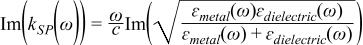
for metal/dielectric junction geometry. Here c, kSP, εmetal(ω), and εdielectric(ω) are the speed of light in vacuum, the complex wavenumber of surface plasmon, the complex dielectric function of metal, and the complex dielectric function of dielectric, respectively. We calculate the surface plasmon response spectrum for gold/SiO2 junction using above formula and show as a green curve in Fig. 2b. The resonance of gold/SiO2 interface occurs at 2.46 eV, which is responsible for maximum absorption. We note that the absorption coefficient is given by the imaginary part of the wavenumber, i.e., α = −2 Im(kSP). Comparing with the photocurrent responsivity spectra, we find coincidence with the surface plasmon resonance, as shown in Fig. 2b. Thus, we can correlate legitimately the relation between the hot carriers generated in the graphene and plasmonic action at the graphene/gold edges. The surface plasmon resonance for gold/air interfaces (2.51 eV) is not much different from that of gold/SiO2 junction.
In order to explain surface plasmon assisted photo-thermoelectricity under zero bias condition, we need more sophisticated theoretical study on the surface plasmon induced hot-carrier generation mechanism for nanostructured or planar d-band metals. Recent theoretical studies show that, for gold metal, both the Hartree-like self-consistent method and the density functional theory predict notable hot hole generation at 2.4–2.8 eV above the Fermi level, depending on the geometry.45,46 In momentum space, it is predicted that gold metal produces almost isotropic hot hole generation at 2.8 eV.46 Moreover, this resonant hot hole generation occurs at the same energy regardless of the layer thickness of the gold film.46 Comparison with these theories allows us to decide which type of carriers are generated and diffused using our experimental data. It is evident that the number of carriers in the gold electrodes is much greater than that of the photoexcited carriers in the graphene owing to huge differences in the density of the states. Fig. 2b shows that "L" mode photocurrent responsivity always generates positive photocurrent values at the edge of the left gold electrode. This means that the current flows from the left electrode to graphene. If hot "electrons" are responsible for the net photocurrent, the sign should be opposite. Therefore, we can conclude that photocurrent generation is due to the hot holes in the gold under zero bias, which is consistent with the theories.
Photocurrent mechanism in "V" mode
In "V" configuration, the photocurrent is collected across the graphene/IGZO junction. The vertical transport properties with top gate under dark condition have been investigated in our previous work.27 The heterojunction works as a low-power-threshold vertical field-effect transistor (VFET) with average current on/off ratio (Ion/Ioff) and on-current density (Jon) on a wafer of ∼3000 and ∼0.09 μA μm−2, respectively.27 We note that the vertical heterostructure forms an asymmetric tunnel junction under zero gate bias.27 Without top gate, our device in the vertical mode can be regarded as photo-gated VFET like other lateral FETs reported for graphene-based devices.47,48 Unlike electrical gating, however, photo-gating does not alter the slope of the Fowler-Nordheim junction potential unless the photoexcited excitons dissociate and move to opposite directions.
The transport properties of an IGZO thin film have been widely studied in the previous literature.23,26,32,49–52 According to the Hall effect measurement, carrier concentration of the pristine IGZO thin film is order of ∼1019 cm−3, but can be increased up to 1020 ∼ 1021 cm−3 by additional Argon treatment.38,53 The doping concentration of the graphene under dark condition can be calculated by gating experiment and capacitance-voltage measurement. The dopant density arising from the gate voltage can be expressed as n = 1/π(E/−hvF)2, where E is the Fermi energy under gate bias and vF ∼ 108 cm/s is the Fermi velocity of the graphene. In our previous work, the Fermi energy shift of 0.34 eV was observed under the gate bias of 42 V by current-voltage characteristics.27 The estimated carrier concentration of the graphene is, therefore, n ∼ 8.5 × 1012 cm− 2.
In the vertical configuration, photocurrent scanning micrographs show unidirectional net current flow from the graphene layer to the IGZO irrespective of the incident light wavelength, as shown in Fig. 2d. The net current flow under illumination primarily originates from the photoexcited carriers in the IGZO layer rather than in graphene, because the density of the states at the top of the valence band of IGZO is larger than that at the Fermi level of graphene. Furthermore, the carrier number density of the IGZO film in dark conditions is at least ten times higher than that of the CVD-grown graphene.49 Note that the unidirectional current flow in our sample is opposite to the case of the graphene/silicon junction.17,19
From the energy-dependent photocurrent microscopy data, several important clues for the photocurrent mechanism in "V" configuration can be extracted. First, high energy illumination generates a larger photocurrent response that is inconsistent with the previously reported photocurrent experiment carried out only on IGZO film as a photon absorbing layer.32 In our work, a maximum of 10.1 μA/W of photocurrent responsivity is obtained with 3.08 eV (403 nm) illumination. This value is the second highest responsivity under zero bias next to graphene/silicon junction.21 The second observation is that, unlike the graphene/silicon junction, there are still non-negligible photocurrents under zero bias, even when the excitation laser energy is lower than the bandgap of the IGZO (up to 3.5 eV). Similar to the previous report on IGZO photodetector, the impurity band over the top of the valence band seems to supply photoexcited carriers.32 Because holes in the IGZO layer are highly localized,24,25,27,38 the majority photocarriers would be electrons. Third, the photocarriers excited near the electrodes hardly contribute to the photocurrent, even though the hot holes are efficiently generated in the electrodes as in "L" configuration. This observation suggests that the carriers excited in the IGZO layer are mostly responsible for the photocurrent.
Considering these observations, we attribute "V" mode photocurrent mechanism to initial high energy carrier generation in the IGZO layer and the subsequent photoelectric diffusion, as illustrated in Fig. 3b. Photons entering the graphene/IGZO junction generate excitons in the IGZO layer. Because of the non-crystalline phase and inelastic scattering centers, electrons and holes lose their kinetic energies quickly.32 While most of holes are trapped inside the IGZO, electrons can be more mobile and be able to diffuse by the assistance of Fowler-Nordheim field.
Currently, it is not clear whether the bottom nickel electrode also provides hot carriers due to the illumination penetrating through the IGZO layer. Our data, at least, do not explicitly exclude this possibility since the photocurrent values increase with the incident laser energy and the electron flow direction is always from the nickel electrode to the graphene layer through the IGZO layer. In order to identify the majority carrier flow between the IGZO layer and the nickel layer, further first-principle calculations, like in the case of gold, are necessary. Ultimately, the diffused carriers from the nickel follow the same relaxation paths as the carriers generated in the IGZO layer, which results in only positive photocurrent values.
Conclusions
We have successfully demonstrated a wafer-scale graphene/oxide semiconductor junction where photocurrent can be collected in dual mode. We observed photo-thermoelectric hot carrier generation in the gold electrode with no external bias in the lateral mode. Coincidence of the photocurrent spectrum with the surface plasmon resonance of gold electrodes and antisymmetric photocurrent microscope images show that hot holes mediated by the surface plasmon of the electrodes are responsible for the major photocarriers in the lateral mode. In the vertical mode, the unidirectional photocurrent is generated opposite to the case of the reported graphene/silicon Schottky junction. The photoexcited electrons in the IGZO layer are majority photocarriers in the vertical mode, which is followed by relaxation and diffusion to the graphene side due to the Fowler-Nordheim potential.