
Abstract
Nonpolar a-plane  GaN (a-GaN) was photo-chemically etched under ultraviolet illumination using alkali KOH solution, and the Ohmic contact properties on the etched a-GaN epitaxial layer were investigated. After photo-chemical etching, the striated surface morphology along the c-axis [0001] direction was obtained having triangular prisms consisting of m-plane
  facets. The properties of Ti/Al/Ni/Au Ohmic contact on surface-textured a-GaN films were studied with transmission line method patterns aligned along the specific crystal orientations. The minimum specific contact resistance of 9.97 × 10⁻⁵ Ω·cm2 was achieved along the c-axis on the etched GaN surface at the annealing temperature of 750°C. The etched a-GaN showed higher electrical conductivity along the c-axis than along m-axis. This anisotropic behavior is in contrast to that of the unetched a-GaN where carrier scattering by basal plane stacking faults in the direction perpendicular to the c-axis is a major factor in determining opposite anisotropic conductivity. The higher conductivity along the c-axis of the etched a-GaN film could be explained by more dominant effect of surface roughness scattering.
Export citation and abstract BibTeX RIS

This is an open access article distributed under the terms of the Creative Commons Attribution 4.0 License (CC BY, http://creativecommons.org/licenses/by/4.0/), which permits unrestricted reuse of the work in any medium, provided the original work is properly cited.
As a wide bandgap compound semiconductor, GaN is one of the most suitable materials for light-emitting diodes, RF and power devices, and bio- and gas sensors.1–15 Particularly in the last decade, there has been a great development in GaN-based high-speed power devices of which material systems show high breakdown voltage and saturation velocity for power switching applications.1,16,17 Conventional c-plane AlGaN/GaN high electron mobility transistor (HEMT) exhibits high breakdown voltage and low on-state resistance due to the high sheet carrier density at the interface between AlGaN and GaN without external doping.11,18 The two-dimensional electron gas (2-DEG) channel formed at the c-plane AlGaN/GaN interface by spontaneous and piezoelectric polarization electric field results in high electron mobility and low on-state resistance, whereas it presents a major challenge for achieving an enhancement mode operation of the transistor. Many efforts have been devoted to realize normally-off devices by controlling the composition and thickness of AlGaN layer, employing a gate recess structure, and implanting fluorine ions on the gate region. However, the normally-off AlGaN/GaN transistors still suffer from high on-state resistance, parasitic resistance, and reliability issues.19–22 As an alternative approach, AlGaN/GaN HEMTs using nonpolar or semipolar GaN crystal structures were investigated, where better control of channel conductivity is expected.6,21,22
Ohmic metal contact is one of the important basic building blocks in fabricating the semiconductor devices. For various crystal planes of hexagonal wurtzite GaN structure, one may expect different properties of metal contacts and electrical conductivity depending on various GaN crystal planes because of the possible influence of different surface atomic configurations, polarization surface charges, effective mass and in-plain strain anisotropy on the metal contact parameters.1,11 In the previous report,11 Baik et al. showed that there existed significant electrical anisotropy in highly-faulted nonpolar a-plane  GaN (a-GaN) film. The in-plane resistance parallel to the c-axis [0001] was approximately two times higher than the one perpendicular to the c-axis due to the carrier scatterings by basal plane stacking faults (BPSFs) along the c-axis direction. Jang et al. also found higher sheet resistances along the
  direction on semipolar
  GaN (s-GaN) film, which can be explained based on the carrier scatterings by BPSFs.13 In addition, the same trend could be observed even in the roughened s-GaN film by photo-chemical etching.18
In this study, we studied the properties of Ti/Al/Ni/Au ohmic contact and its electrical anisotropy on the surface-textured a-GaN films with transmission line method (TLM) patterns designed with different azimuth angles. The lowest specific contact resistances were obtained at 750°C annealing for 1 min under N2 ambient. We found that the sheet resistance along the m-axis direction was higher than the one along the c-axis, which was opposite to the unetched a-GaN films.18
Experimental
Nonpolar a-GaN epitaxial layers with 4 μm in thickness were grown on r-plane  sapphire substrates by an AIX 2400 G3 metal organic chemical vapor deposition system with a planetary reactor.2,23 Trimethylgallium and ammonia were used as gallium and nitrogen sources, respectively. The sapphire substrates were thermally cleaned at 1050°C for 10 min prior to the growth, and the surface nitridation was performed with an ammonia flow of 8 slm (standard liter per minute). High-temperature 150-nm-thick GaN nucleation layer was grown in mixed atmosphere of H2 and N2 at the temperature of 1050°C to reduce dislocation density and to obtain the minimum surface roughness. Subsequently, a-GaN epitaxial layer with high crystalline quality was obtained by the conventional two-step growth method. During the three-dimensional island growth, multiple SiNx layers were inserted by flowing SiH4 and NH3 to improve crystalline quality. The surface orientation and crystalline quality of as-grown a-GaN films were characterized by high-resolution X-ray diffraction, using Jordan Valley QC3 system with a Cu Kα1 X-ray target source (λ = 1.5406 Å). The full width at half maximum values of the X-ray rocking curve for the grown a-GaN films were measured to be 450 and 620 arcsec along the c-axis and m-axis directions, respectively. The electron concentration and the mobility obtained from Hall measurements with van der Pauw method were ∼3 × 1018 cm−3 and 127 cm2/V·s.
For photo-chemical etching, the as-grown a-GaN samples were immersed in 1 M KOH solutions and exposed to ultraviolet light (UV) by using an Excelitas X-cite 120PC Q, 120 W mercury lamp for 5 min. After photo-chemical etching, the sample was rinsed with deionized water thoroughly. The surface morphology of the photo-chemically etched a-GaN film was analyzed by field-emission scanning electron microscopy (SEM) and atomic force microscopy (AFM).
Ohmic contacts consisted of Ti (200Å)/Al (800Å)/Ni (400Å)/Au (800Å) deposited by an electron beam evaporator and patterned by lift-off to form transmission line method (TLM) patterns with 100 × 100 μm pads separated by spacing from 2–16 μm. The TLM patterns were oriented along either the c-axis [0001] and the m-axis  directions (Figure 1d). These contacts were subsequently annealed at temperatures from 300 to 1000°C for 1 min under flowing N2 in a rapid thermal annealing (RTA) system. The current-voltage (I-V) characteristics of the etched a-GaN were measured using an Agilent 4155C semiconductor parameter analyzer. The ohmic contact properties, specific contact resistance and sheet resistance wereobtained from linear TLM measurements.2
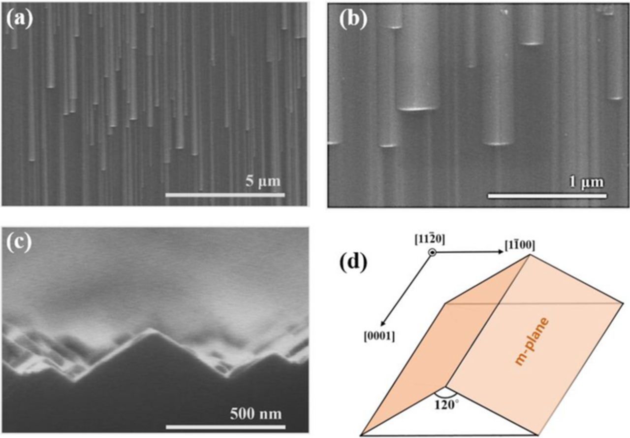
Figure 1. (a), (b) Top and (c) cross-sectional view SEM images of photo-chemically etched a-GaN, (d) schematic diagram of the etched a-GaN crystal planes.
Results and Discussion
Figures 1a and 1b show top-view SEM images of photo-chemically etched a-GaN surface at low and high magnification, respectively. The striated surface morphology along the c-axis direction was obtained showing numerous triangular prisms. An isosceles triangle with 120 degrees was found in the cross-sectional SEM image of the prism as shown in Figure 1c. The etched surface morphology has the shape of nano-sized prisms with a triangular cross-section consisting of two m-plane  facets on a-plane
  base, where the angle between m-planes is 120 degrees, for example, between
  and
and  planes (Figure 1d). Hence, m-planes of GaN were exposed after photo-chemical etching of a-GaN film.9
The AFM image of photo-chemically etched a-GaN is shown in Figure 2. Distinctive ridges aligned parallel to the c-axis direction were observed. The root mean square (RMS) roughness over a scan range of 5 × 5 μm2 is 26.86 nm, which is noticeably larger than 2.31 nm of as-grown a-GaN film. Photo-chemical etching of GaN is a repetitive process involving the formation of gallium oxide and dissolution of the oxide in an alkali etchant solution. During this etching process, stable crystal planes with low surface energy are etched slower than unstable planes with high surface energy, which determines the specific crystal planes exposed after photo-chemical etching.24 The surface energy of m- and a-GaN are 118 and 124 meV, respectively.5,25 Therefore, more stable m-GaN surface would be likely to be exposed after the photo-chemical etching, resulting in the triangular prismatic surface morphology.
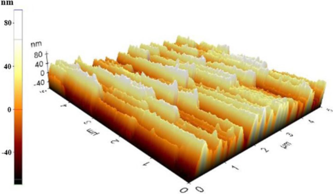
Figure 2. Atomic force microscopic image of photo-chemically etched a-GaN with a root mean square roughness of 26.86 nm.
Figure 3 shows the representative I-V characteristics depending on annealing temperatures for the 2 μm gap TLM pads oriented parallel to the c-axis direction. The Ohmic contact behaviors were observed from the annealing temperature of 600°C, and the minimum total resistances were found at the temperature of 750°C for both TLM metal pads in the c- and m-axis directions. Figure 4 shows the specific contact resistances as a function of annealing temperatures for respective TLM pads in the c- and m-axis directions. In both cases, the specific contact resistances decreased with increasing the annealing temperature up to 750°C with the lowest specific contact resistances of 9.97 × 10⁻⁵ and 1.03 × 10⁻⁴ Ω·cm2 for the c- and m-axis directions, respectively, and then increased at higher temperatures. This dependence of specific contact resistance on annealing temperature for photo-chemically etched a-GaN is similar to that previously reported for the unetched a-GaN.11
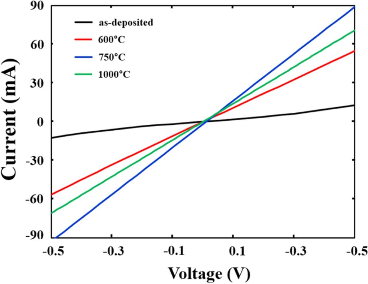
Figure 3. I–V characteristics between contact pads in the TLM pattern as a function of annealing temperature for the TLM pattern parallel to the c-axis direction.
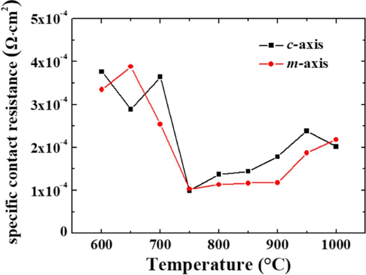
Figure 4. Specific contact resistance of photo-chemically etched a-GaN as a function of annealing temperature for the TLM patterns oriented in both c- and m-axis directions.
Figure 5 presents the sheet resistances for the c- and m-axis oriented TLM pads on the etched a-GaN annealed at different temperatures. Note that the sheet resistance parallel to the c-axis direction is lower than the one along the m-axis direction, which is contrast to the previous findings in the unetched a-GaN.11 In the case of the unetched a-GaN, BPSFs with very thin zinc blende layer exist perpendicular to the c-axis direction. The band offset of 270 meV at the interface between BPSF and wurtzite GaN matrix induces dominant carrier scattering along the c-axis direction, thereby resulting in higher sheet resistance along the c-axis than the m-axis directions.26–28 The similar characteristics of lower sheet resistance along the m-axis direction than the one along the  direction for s-GaN was also reported due to the carrier scattering by BPSFs.13 Although the sheet resistance ratio, the sheet resistance along the
  direction over the one along the m-axis direction, decreased from 2.08 to 1.63, even the photo-chemically etched s-GaN with RMS roughness of 24.58 showed better lateral conductivity in the m-axis direction.18 Surface roughness scattering along the carrier transport direction from the surface morphology would be one of main factors in determining the anisotropic electrical conductivity of photo-chemically etched a-GaN. After photo-etching of s-GaN, trigonal prisms with (001) and (100) planes were observed. In the case of a-GaN, straight stripes with triangular prisms perpendicular to the m-axis were obtained after photo-chemical etching as shown in Figure 1, and the etched a-GaN had the surface morphology showing more surface roughness scattering along m-axis. For the as-grown a-GaN, BPSF-induced carrier scattering is responsible for lower sheet resistance along the m-axis. In contrast, the surface roughness scattering from the etched surface is the dominant factor in the higher conductivity in c-axis direction of the photo-chemically etched a-GaN.
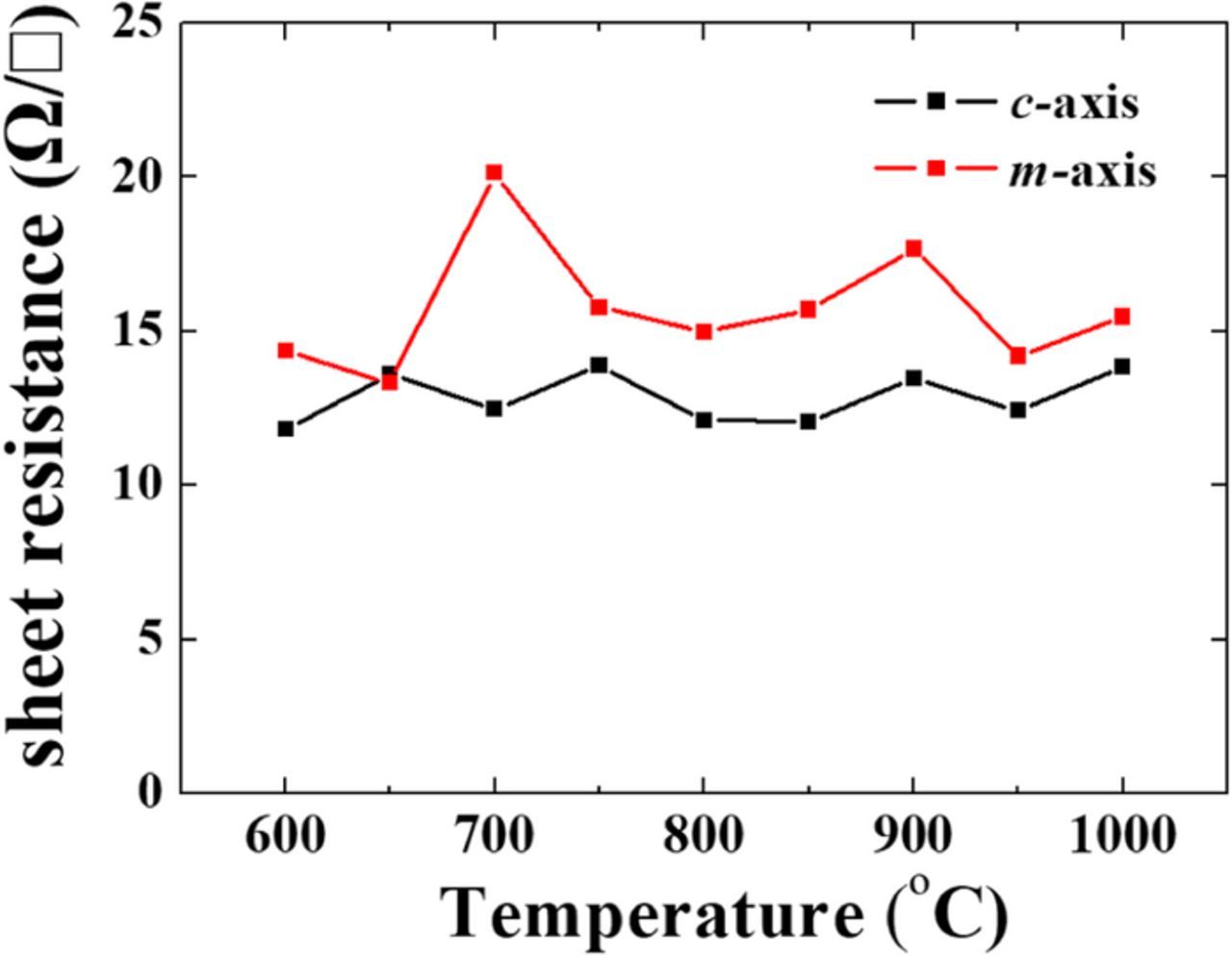
Figure 5. Sheet resistance of photo-chemically etched a-GaN as a function of annealing temperature for the TLM patterns oriented in both c- and m-axis directions.
Figure 6 shows optical microscope images of contact pads (a) as-deposited and annealed at (b) 750°C, (c) 900°C, and (d) 1000°C. The morphology of metal contact is relatively smooth until 750°C, which is corresponding to the minimum specific contact resistance at 750°C as shown in Figure 4. This is possibly related to the formation of low resistance phases of TiN at the interface with a-GaN.11 At higher annealing temperature, extensive intermixing of the contact metallurgy occurs and the metal morphology roughens and degrades as the EDAX mapping of Ti, Al, Ni, and Au indicates.
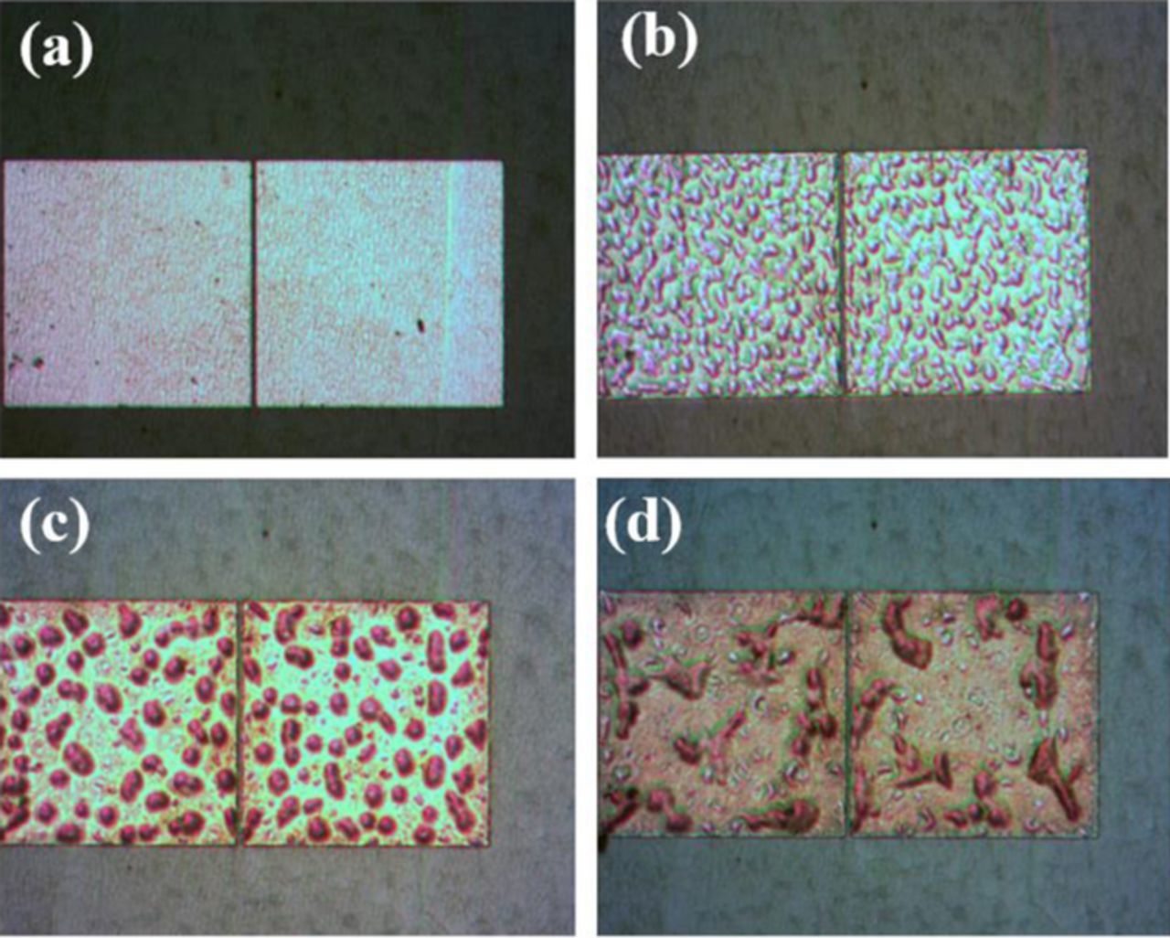
Figure 6. Optical microscope images of metal contact pads at different annealing temperatures for the c-axis oriented TLM patterns: (a) as-deposited and annealed at (b) 750°C, (c) 900°C, and (d) 1000°C.
Conclusions
Nonpolar a-GaN was etched by photo-chemical wet etching, and the Ohmic contact properties at different annealing temperature were investigated. The surface morphology of the etched a-GaN showed straight stripes consisting of triangular prism with m-plane facets along c-axis. The lowest specific contact resistance of 9.97 × 10⁻⁵ Ω·cm2 was obtained along the c-axis oriented TLM pads at the annealing temperature of 750°C. The sheet resistance parallel to the c-axis direction is lower than that in the m-axis, which is in sharp contrast to the as-grown a-GaN, and the unetched or etched semipolar s-GaN. This attributes to the dominant effect of the surface roughness scattering on the textured surface morphology rather than the carrier scattering due to BPSFs perpendicular to c-axis.
Acknowledgments
The present research was conducted by the research fund of Dankook University in 2017.