
Abstract
This study examined the effects of the Zn ratio on the microstructure of InGaZnO (IGZO) films and the device performance of their transistors. IGZO films with various Zn ratios were produced by co-sputtering InGaO and ZnO at different ZnO powers. The combination of transmission electron microscopy (TEM) and X-ray diffraction (XRD) analyses elucidated that as the Zn ratio increased from 0 to 0.69, the microstructure changed from amorphous IGZO to nanocrystalline IGZO and then to columnar ZnO. The dynamic transitions of the microstructure, in turn, profoundly affected the electrical properties including the mobility and carrier concentration. The sample with a mixing ratio of 0.25:0.2:0.55 (In:Ga:Zn) exhibited the best performance with a mobility of nearly 30 cm2/V·s.
Export citation and abstract BibTeX RIS
Transparent oxide semiconductors (TAOS) have recently gained much attention owing to their technologically important features, including their high electron mobility, high transparency, capability for low temperature processing, etc. These materials are excellent candidates for the active layer of thin film transistors for display applications.1, 2 In particular, amorphous InGaZnO4 (IGZO) has been the focus of many research and development efforts since Hosono and colleagues first demonstrated the possibility of using it as the active layer of TFTs.3 Some such studies include the optimization of sputtering conditions (O2 pressure, sputtering power, etc) and post-annealing conditions.1, 4 Nevertheless, systematic composition engineering of this material by modulating the cation ratio still remains incomplete.
For the development of IGZO-based transistors with enhanced device performance, it is important to understand the roles of the main metallic elements (In, Ga, and Zn) of the material. Some recent studies unfolded that as the In ratio increased, the carrier concentration escalated sensitively and thus led to an increase in both the on-current and off-current, suggesting that In played the role of charge carrier generators.5, 6 Increasing the Ga ratio seems to have the opposite effect: With the Ga content increasing, the carrier concentration drastically decreases since Ga suppresses oxygen vacancy formation.5–10 Thus, the In/Ga ratio is known to be critical for determining the carrier concentration of IGZO films. However, what remains relatively unexplored are the effects of modulating the Zn ratio on the film properties. It would be intriguing to investigate how the microstructure evolves and the electrical properties change as the Zn ratio changes over a wide range.
In this study, we delved into the effects of the Zn ratio on the characteristics (microstructure, carrier concentration, and Hall mobility) of IGZO films and the device performance of their TFTs. We produced IGZO films with various Zn ratios via co-sputtering InGaO (IGO) and ZnO at different ZnO target powers. Combining X-ray diffraction (XRD), transmission electron microscopy (TEM), and Hall Effect measurements helped us to fully characterize the evolution of the film microstructure and properties with the addition of Zn.
Experimental
We fabricated IGZO-based TFTs with a simple bottom-gated structure by utilizing a highly-doped p-type Si substrate with a resistivity of 0.001–0.005 Ω cm for the gate electrode. A silicon nitride film with a thickness of 400 nm was deposited using plasma enhanced chemical vapor deposition (PECVD) on the substrate as the gate dielectric. Subsequently, we co-sputtered a 70 nm-thick IGZO layer from In2O3-Ga2O3 (purity of 99.99% with the mixing ratio of In2O3 50 wt %: Ga2O3 50 wt %) and ZnO (purity of 99.99%) targets at a working pressure of 5 mTorr and a flow ratio (O2/Ar) of 0.4% in a radio frequency (rf) magnetron sputtering system. The target size was 3 in. in diameter. For the control of the Zn ratio, the RF power for the ZnO target was modulated from 0 to 150 W while that for the InGaO (IGO) target was fixed at 100 W. The thicknesses of the cosputtered films were maintained at nearly the same values, around 70 nm. The active region was patterned with a size of 550 × 1000 μm via lift-off. The samples were then annealed at 300°C in air for 1 h in a furnace. For the formation of source-drain electrodes, Mo was sputtered and patterned by lift-off. The channel length and width were 50 and 100 μm, respectively.
The carrier concentration and electron mobility of the films were measured using a Hall Effect measurement system (Accent HL5500). The electrical characteristics of the transistors were measured using an HP semiconductor parameter analyzer (HP4145B). We utilized XRD (X'pert PRO MRD) and TEM (JEOL, JEM2100F operating at 200 keV) to characterize the microstructures of the co-sputtered IGZO films. In addition, we used X-ray photoelectron spectroscopy (ESCA 2000) for the composition analysis of the co-sputtered films.
Results
Microstructure analysis
Table I shows the composition analysis results of the co-sputtered films of IGO and ZnO, disclosing that the Zn ratio (Zn/(In+Ga+Zn)) sensitively varies widely from 0 to 0.69 with the sputtering power of the ZnO target while the In/Ga ratio changes only a little. Thus the composition variation follows systematically along the line indicated in the ternary diagram shown in Fig. 1. Next, we used XRD to examine how the microstructure of the films changes as the Zn ratio increases from 0 to 0.69. Figure 2 shows the XRD curves taken from two sets of the films, one for the as-deposited films and the other for the samples post-annealed at 300°C. The XRD curves of the films annealed at 300°C are nearly the same as those of the as-deposited samples.
Table I. Summary of the cation ratio of the three metallic elements (indium, gallium, and zinc) as a function of the ZnO rf power.
| rf power of ZnO target | 0 W | 20 W | 50 W | 80 W | 100 W | 120 W | 150 W |
|---|---|---|---|---|---|---|---|
| In/(In+Ga+Zn) | 0.54 | 0.48 | 0.36 | 0.25 | 0.25 | 0.20 | 0.16 |
| Ga/(In+Ga+Zn) | 0.46 | 0.43 | 0.32 | 0.25 | 0.20 | 0.18 | 0.15 |
| Zn/(In+Ga+Zn) | 0 | 0.09 | 0.32 | 0.5 | 0.55 | 0.62 | 0.69 |
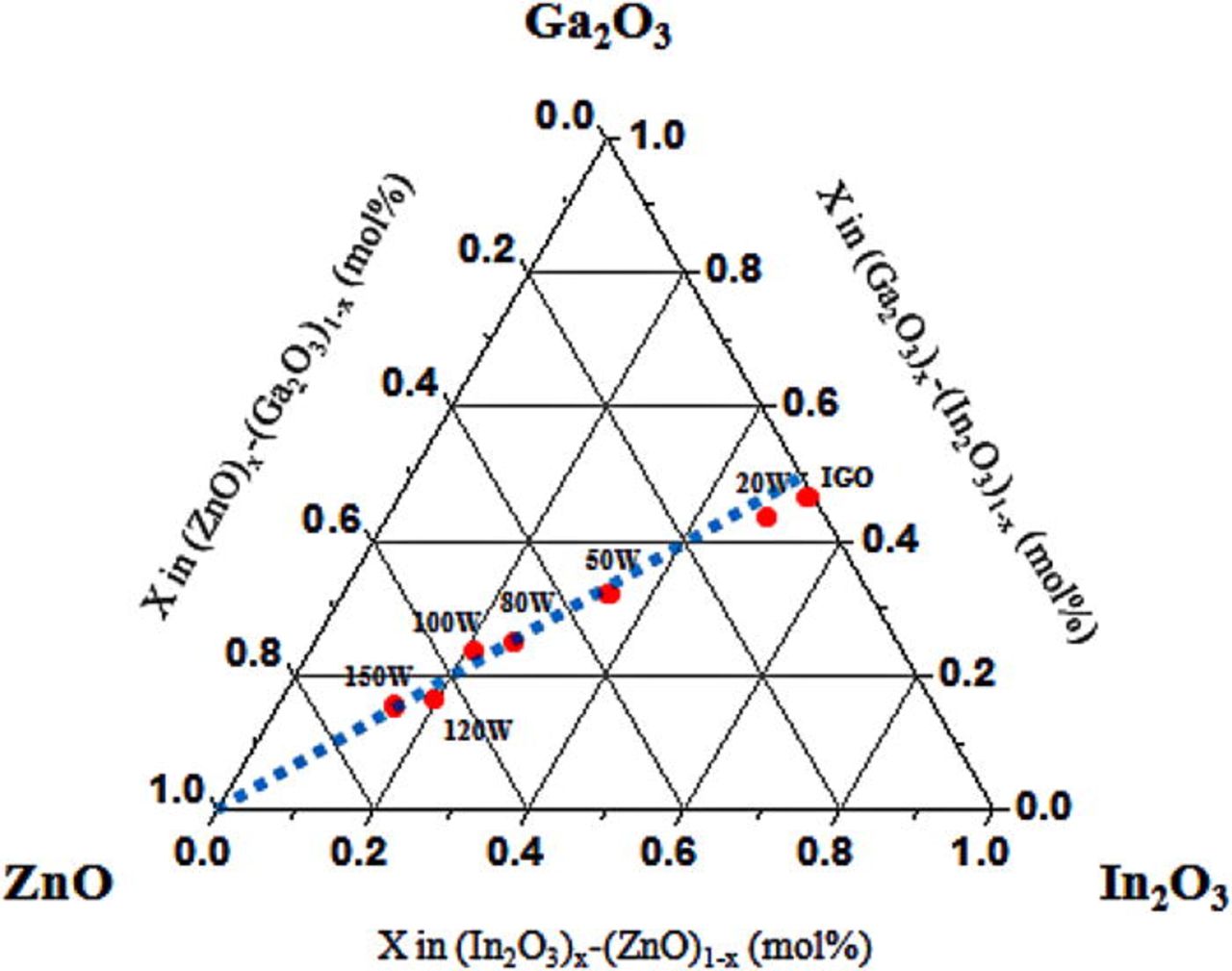
Figure 1. (Color online) A ternary diagram that maps the compositions of the samples used in this study.
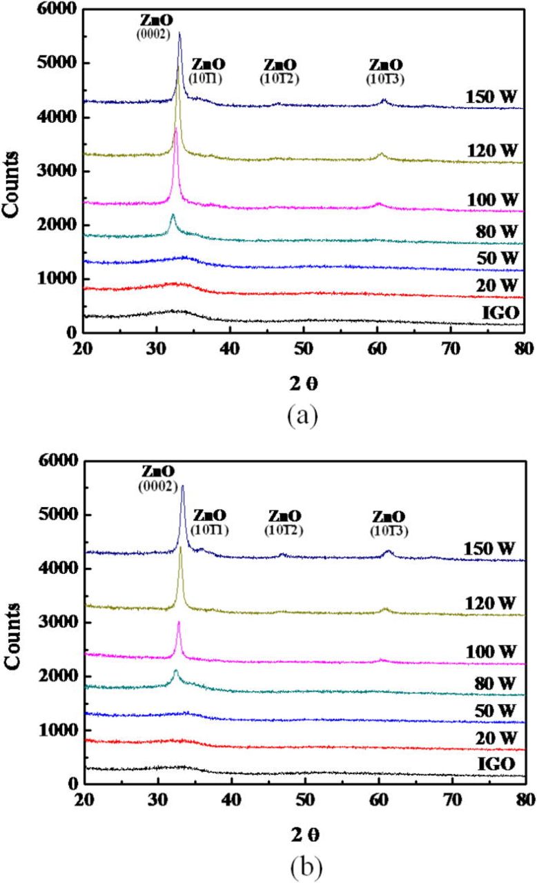
Figure 2. (Color online) XRD data of the IGO and co-sputtered IGZO films, (a) as-deposited and (b) annealed at 300°C.
The sample with no Zn content (that is, the IGO sample) displays a broad peak with a low intensity near 34°, which indicates that the film is amorphous. This appearance does not change much until the Zn ratio increases up to 0.32 for the sample deposited at a ZnO target power of 50 W. For the 80 W sample, a small peak emerges around 32° from the broad amorphous peak and the peak position is close to that of the (0002) reflection of the hexagonal ZnO phase.11 For the films deposited at higher ZnO powers, the peak rises stronger and shifts close to the ZnO (0002) reflection (34.4°), and an additional peak appears around 62°, a peak position closely matching that of the (10–13) reflection of ZnO. Finally, the sample with the highest Zn ratio (150 W sample) shows several additional small peaks pertaining to the ZnO phase, which indicates that the film fully transformed to the ZnO phase. Overall, these XRD results suggest that as the Zn content increased, the phase of the film shifted from amorphous to the ZnO phase.
TEM characterization helped us to elucidate the details of the microstructure evolution of the co-sputtered IGZO films with the systematically increasing Zn ratio. Figure 3a shows bright-field and high-resolution electron micrographs obtained from the IGO film. The bright-field image displays a gray-colored, featureless appearance and the high resolution image shows a completely disordered amorphous structure. The microstructure of the 50 W sample with a substantial amount of Zn (In:Ga:Zn = 0.36:0.32:0.32), shown in Fig. 3b, displays a similar amorphous structure.
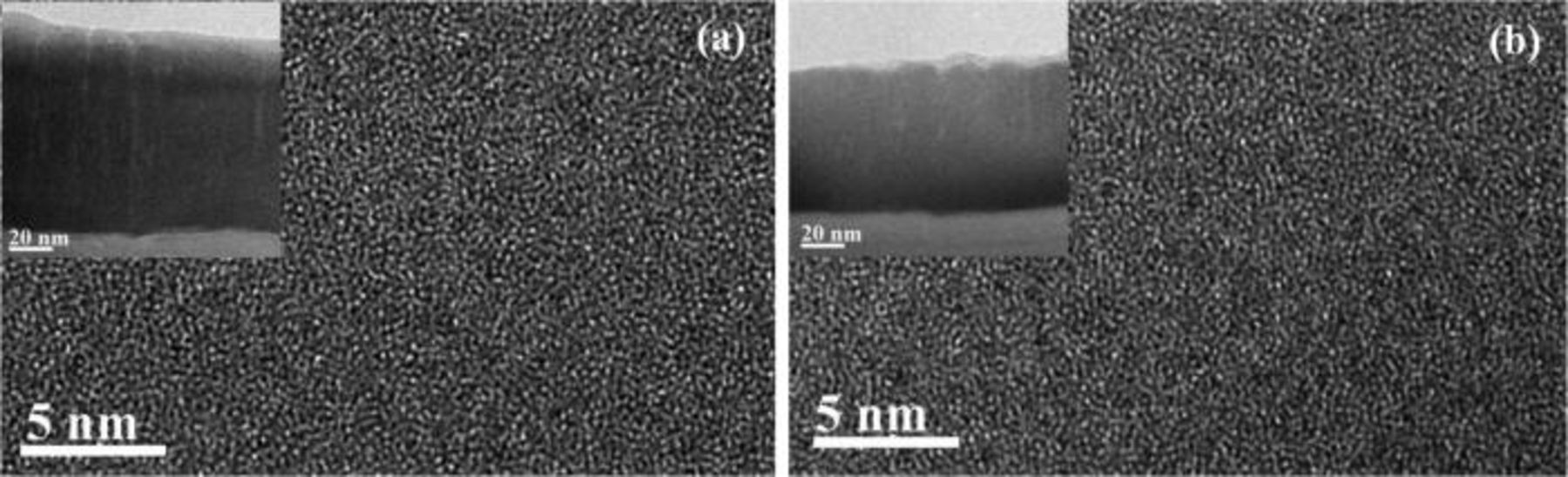
Figure 3. High-resolution electron micrographs of the IGO (a) and 50 W samples (b). The insets show the bright-field electron micrographs.
In Fig. 4, the 80 W sample also appears in a uniform contrast in the bright-field image, but the high-resolution image discloses a microstructure different from a disordered structure, in which atomic ordering is prevalent and nanometer-sized grains are widely distributed. To understand the nature of the nanocrystalline grains, we carried out compositional mapping on the area using EDS. (The electron beam size used for the EDS analysis was 0.7 nm.) Figure 4c shows the distribution of the three metallic elements, In, Ga, and Zn, demonstrating that the distribution of the three metallic elements is quite uniform. The homogeneous distribution of the elements confirms that raising the Zn ratio close to 0.5 did not prompt the phase separation of ZnO from amorphous IGZO, but rather possibly enhanced the atomic order to convert the amorphous structure to nanocrystalline IGZO. Nevertheless, it should be mentioned that there exist some grains (with lattice fringes with a plane spacing corresponding to that of (0002) planes of ZnO) near the top of the film, as denoted by the arrows in Fig. 4a, suggesting the formation of ZnO grains at the later stage of film growth. These results are consistent with those of the XRD analysis in that the small ZnO peak arises from the ZnO grains formed near the top while the broad IGZO peak corresponds to the nanocrystalline IGZO.
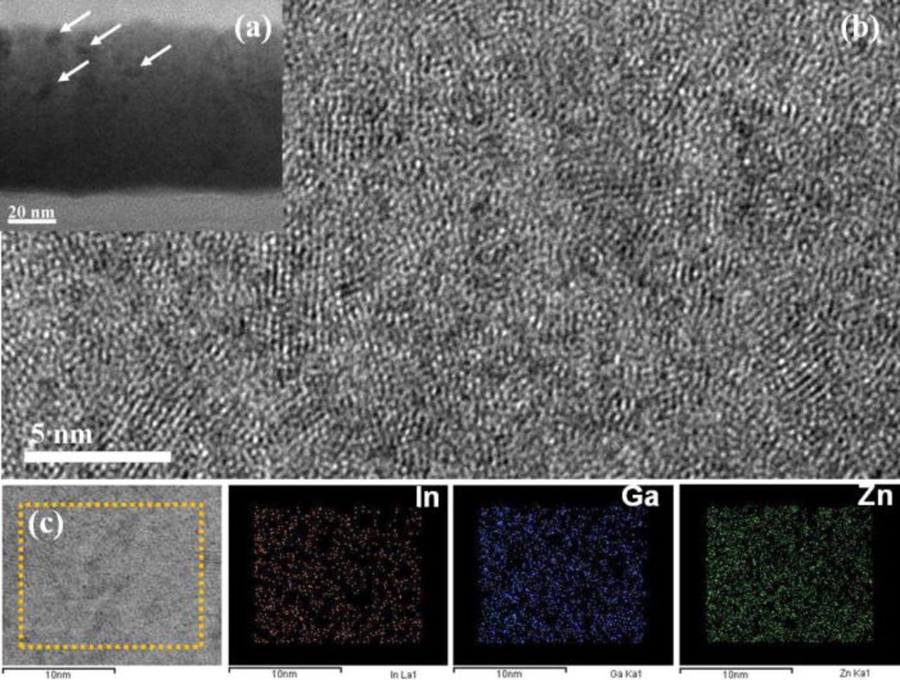
Figure 4. (Color online) Electron micrographs of the 80 W sample. (a) Bright-field electron micrograph, (b) high resolution electron micrograph, and (c) compositional mapping obtained from EDS analysis. The compositional map was acquired from the rectangle marked in the bright-field scanning transmission electron microscopy (STEM) image.
As the Zn ratio increased to 0.55 for the 100 W sample, the microstructure became drastically different. In the bright-field image shown in Fig. 5a, the overall film morphology displays a bi-layer structure in which a thin layer of a uniform contrast lies at the bottom and a columnar structure dominates at the top. Figure 5c, taken from the bottom layer, shows that the layer comprises nanocrystalline grains. Elemental mapping using EDS also indicated that the three metallic elements (In, Ga, and Zn) were uniformly distributed in the layer, suggesting that the layer was nanocrystalline IGZO (elemental map not shown here). Relatively large grains grew vertically from the layer to develop into a columnar structure, as shown in Fig. 5b. The electron diffraction pattern (shown in the inset) displays several rings, the diameters of which closely match those of the (0002), (10–11) and (10–12) reflections of ZnO. In addition, chemical analysis using EDS elucidated the presence of a significant amount (10–15%) of In and Ga in the grains. These results suggest that these columnar grains are ZnO grains dissolving some In and Ga, probably in a manner similar to Ga-doped ZnO, in which the Ga atoms occupy substitutionally some of the Zn sites of the ZnO.12 Thus, the TEM analysis of the 80 W sample leads to a conclusion that the film grew initially as nanocrystalline IGZO and later developed into columnar ZnO grains dissolving some In and Ga.
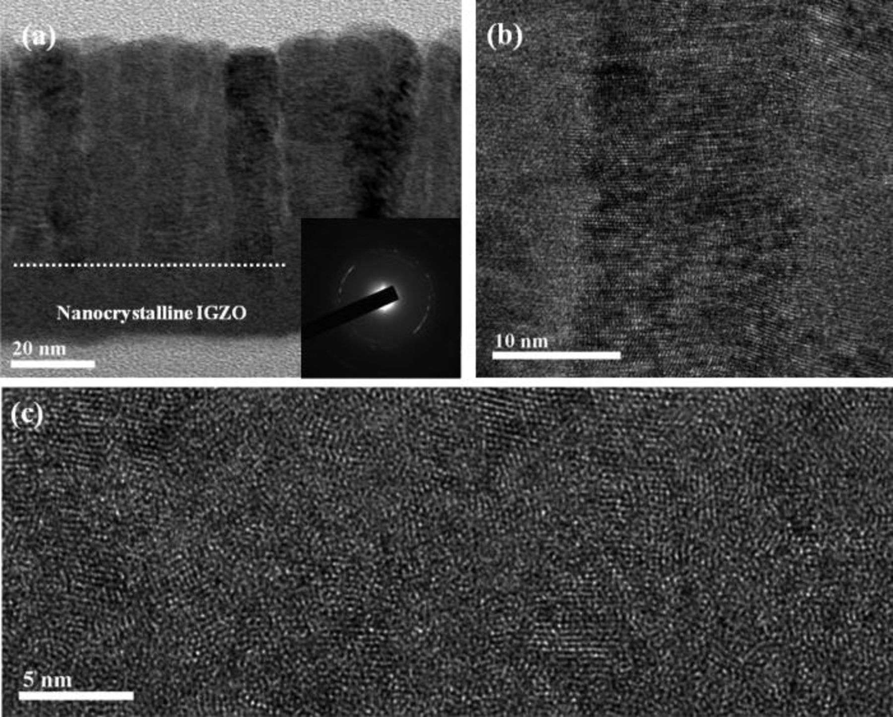
Figure 5. Electron micrographs of the 100 W sample. (a) Bright-field electron micrograph (the inset shows an electron diffraction pattern), (b) high resolution electron micrograph taken from the columnar grains, and (c) high resolution electron micrograph taken from the nanocrystralline grains.
Finally, we examined the 150 W sample with a Zn ratio of 0.69. Figure 6a shows a microstructure that appears similar to a typical ZnO film with vertically grown columnar grains. The electron diffraction pattern, shown in the inset, also matches that of the hexagonal ZnO phase. Chemical analysis using EDS also revealed the presence of some In and Ga in the columnar grains (EDS data not shown here). These results indicate that the 150 W sample grew as the columnar ZnO structure from the initial stage of the deposition. The microstructure analysis of the co-sputtered films with various Zn ratios using XRD and TEM offers a detailed description about the microstructural evolution of the films as the Zn ratio increases from zero to 0.69, as illustrated in Fig. 7. As the Zn content increased, the microstructure first changed from amorphous IGZO to nanocrystalline IGZO, which suggests that the atomic order improved with the Zn ratio increasing. As the Zn ratio increased further, the nanocrystalline IGZO turned into columnar ZnO with some dissolved In and Ga, implying that there is some critical Zn ratio above which the film would grow as the ZnO phase.
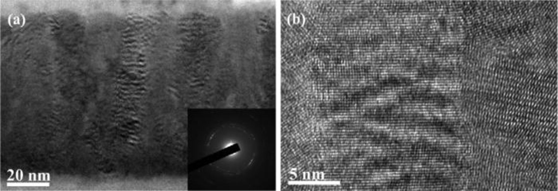
Figure 6. Electron micrographs of the 150 W sample. (a) Bright-field electron micrograph (the inset shows an electron diffraction pattern) and (b) high resolution electron micrograph.
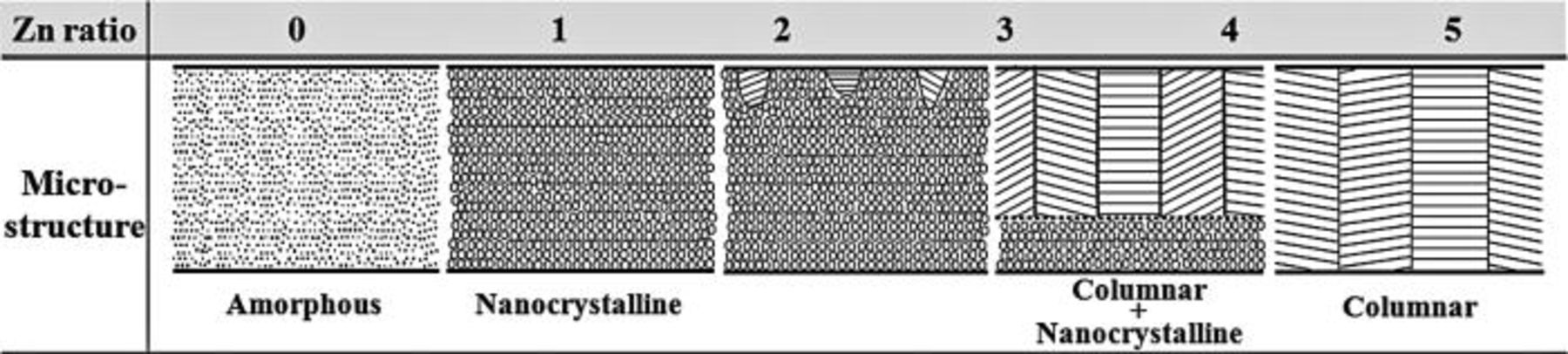
Figure 7. A schematic diagram that illustrates the microstructure evolution of the IGZO co-sputtered films with the Zn ratio increasing.
Electrical characterization
We utilized Hall Effect measurements to estimate the carrier concentration and electron mobility of the co-sputtered films. Figure 8 shows how the carrier concentration and Hall mobility of the films change with the Zn content increasing. The carrier concentration is very low for the sample with no Zn content (that is, the IGO sample), but escalates gradually with the ZnO power increasing up to 80 W. As the ZnO power reaches 100 W, the carrier concentration arises sharply close to 3 × 10¹⁶/cm3 and then gradually increases for the samples with higher ZnO powers (120 and 150 W). The Hall mobility continues to increase substantially to nearly 11 cm2/V·s for the 80 W sample, then drastically drops for the 100 W sample and remains low for the 120 and 150 W samples.
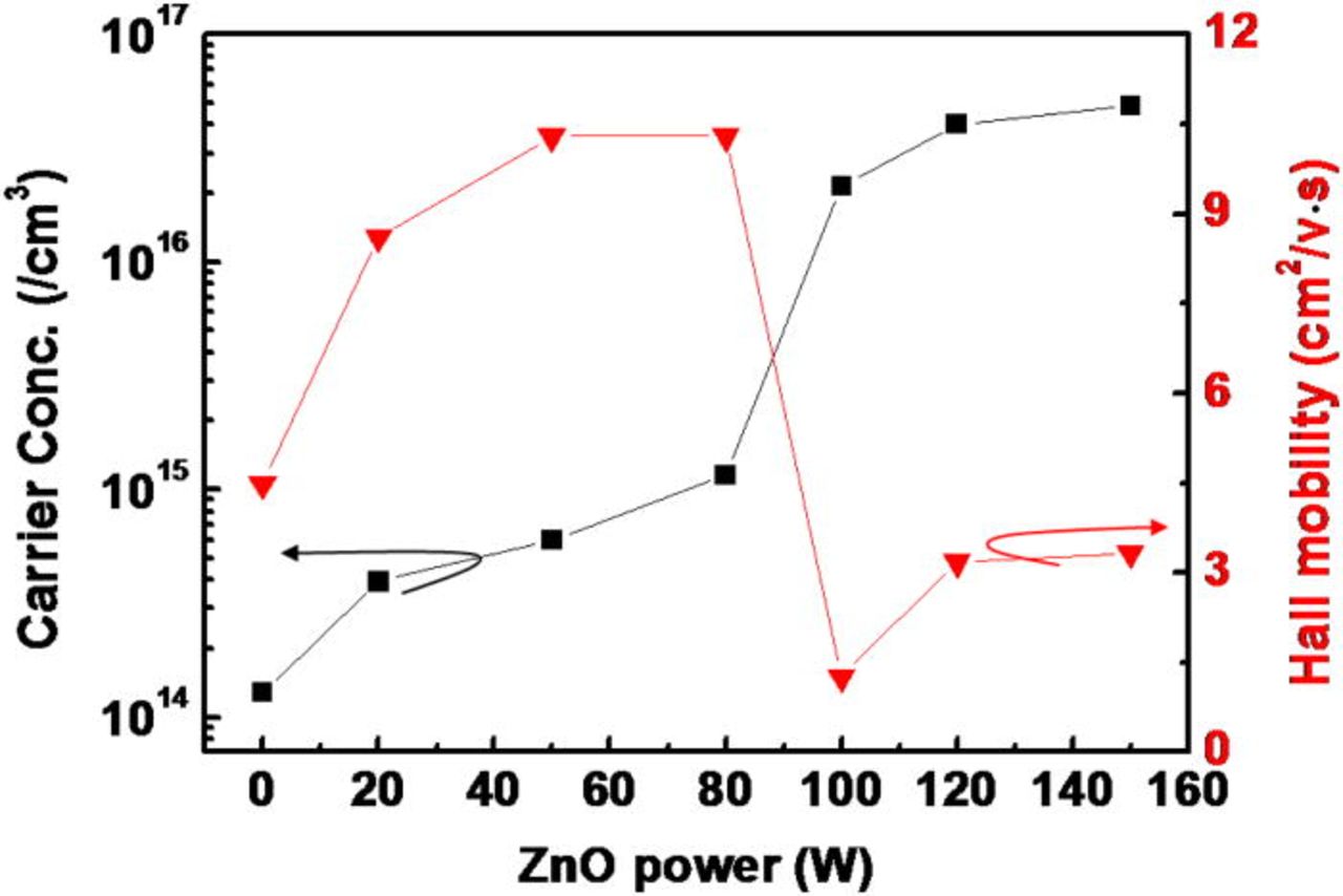
Figure 8. (Color online) Carrier concentration and Hall mobility of the co-sputtered IGZO films.
A notable aspect of the graph is that for a wide range of the Zn ratio (from 0 to 0.55), the Hall mobility increases substantially while the carrier concentration remains low. Nevertheless, both the carrier concentration and mobility change abruptly when the ZnO power reaches 100 W (that is, when the Zn ratio is raised close to 0.55). This abrupt property transition seems coincidental with the microstructure change from nanosrystalline IGZO to columnar ZnO that contains dissolved In and Ga, suggesting that the phase change might be responsible for the abrupt changes of the carrier concentration and mobility.
It is well known that for Ga-doped ZnO, the dissolved Ga atoms substitutionally occupy some of the Zn lattice sites of the ZnO crystal structure, donating their extra electrons and hence leading to a high carrier concentration.13–15 Thus, phase change from nanocrystalline IGZO to ZnO dissolving In and Ga would bring about an abrupt increase in carrier concentration. The phase change is also likely to fundamentally influence the mobility. The mobility values reported for IGZO-based transistors are in general significantly higher than those for ZnO-based transistors, which suggest superior electronic transport in IGZO.14, 16, 17 Thus, it seems possible that phase change from nanocrystalline IGZO to ZnO would cause a drastic drop in Hall mobility.
Next, we characterized the electrical properties of the transistors fabricated from the co-sputtered samples, as shown in the transfer curves (measured at a fixed drain voltage of 10 V) of Fig. 9. Until the ZnO power reaches 100 W, the change of the transfer curve seems rather gradual with the on-current increasing steadily and the turn-on voltage shifting only slightly. However, as the ZnO power rises further, the curve swings abruptly in the negative direction and the on-current drops substantially. The summary of the device characteristics extracted from the transfer curves is shown in Table II. With the ZnO power increasing, the field-effect mobility (μFE) surges strongly up to around 28 cm2/V·s, followed by a drastic drop to 1–2 cm2/V·s for the 120 and 150 W samples. The threshold voltage remains steadily around 2–3 V, and swings to a largely negative value (−16.3 V) as the ZnO power was raised to 120 W and 150 W.
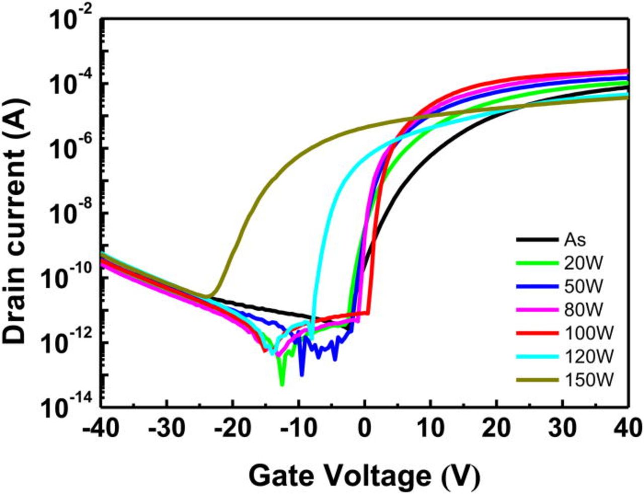
Figure 9. (Color online) Transfer curves of TFTs fabricated from the co-sputtered IGZO films. The data were measured at a fixed drain voltage of 10 V.
Table II. Summary of the electrical properties estimated from the transfer curves shown in Fig. 9.
| μEF (cm2/V s) | Subthreshold slop (V/decade) | Threshold voltage (V) | Ion/off ratio | |
|---|---|---|---|---|
| IGO | 5.70 | 1.25 | 9.3 | 2.9E + 7 |
| 20 W | 7.17 | 0.79 | 3.7 | 2.1E + 9 |
| 50 W | 11.22 | 0.79 | 2.4 | 1.5E + 9 |
| 80 W | 20.77 | 0.46 | 2.1 | 1.5E + 9 |
| 100 W | 28.95 | 0.34 | 3.1 | 5.0E + 8 |
| 120 W | 2.47 | 0.57 | −4.6 | 1.0E + 8 |
| 150 W | 1.24 | 2.17 | −16.3 | 2.5E + 6 |
One important feature of the data is the drastic enhancement of μFE with the increase of the Zn content, reaching close to 30 cm2/V·s. This is much higher than those reported for IGZO TFTs with a typical metallic element ratio (for example, ∼6–9 cm2/V·s for In:Ga:Zn = 1:1:0.9 and 12 cm2/V·s for In:Ga:Zn = 1.1:1:0.7).3, 16 The overall device performance improved steadily up to 100 W, beyond which the device characteristics deteriorated suddenly, similarly to the trend observed in the Hall measurements. These property changes seem very intimately connected to the microstructure changes observed in the TEM and XRD characterization. As the Zn content increased, the atomic order probably enhanced and nanocrystalline IGZO emerged, which would lead to a continuous increase in mobility by reducing the trap density.17–19 However, raising the Zn ratio to a level greater than a critical point prompted a drastic phase transformation from nanocrystalline IGZO to columnar ZnO, resulting in a steep drop in electron mobility and a drastic shift in threshold voltage.
It is worthwhile mentioning that although the Hall measurement and transistor data are, in general, consistent with each other, the points where the electrical properties suddenly change are not exactly the same: 120 W for the transistor data and 100 W for the Hall data. That is, the 100 W sample exhibited excellent transistor characteristics while it displayed a low mobility in the Hall measurements. We suggest that this disparity is possibly due to the unique microstructure of the 100 W sample, a bi-layer structure with a columnar ZnO structure at the top and a nanocrystalline IGZO layer at the bottom. It should be noted that Hall measurements typically detect the bulk properties of a semiconductor film while transistor characterization measures electronic transport along a thin channel layer confined near the interface with the gate dielectric layer. For the 100 W sample with such a bi-layer structure, thus, the Hall measurement data could appear to be significantly different from the characteristics measured from the transistors.
The TEM and XRD analyses allowed us to fully understand how the microstructure of the co-sputtered films of InGaO and ZnO evolved as the mixing ratio varied widely from 0.54:0.46:0 (= In:Ga:Zn) to 0.16:0.15:0.69. As the Zn ratio increased, the microstructure is changed from amorphous IGZO to nanocrystalline IGZO and then to columnar ZnO with some dissolved In and Ga. The electrical properties measured from the Hall measurements and the transistors sensitively reflect the dynamic transitions of the microstructure. The mobility continued to enhance substantially with the threshold voltage changing only slightly as the microstructure changed from amorphous to nanocrystalline. This continuous increase of the mobility ended abruptly when the microstructure changed to columnar ZnO. Nevertheless, it should be noted that the field-effect mobility increased from 5.7 cm2/V·s to nearly 30 cm2/V·s as the Zn ratio was raised from 0 to 0.55 without significantly affecting the threshold voltage or the on/off current ratio. In addition, an active layer with an amorphous structure is often desired for the production of an active matrix with an excellent uniformity. In our study, the samples with high performance exhibited a nanocrystalline structure with a grain size in the range of only several nanometers. It is likely that such a structure would also display a good uniformity, since the grain size is very uniform and extremely small compared with the size of the active area.
Summary
In this study, we examined the effects of the Zn ratio on the microstructure of IGZO films and the device performance of their transistors by producing IGZO films with various Zn ratios via co-sputtering IGO and ZnO. TEM and XRD characterization illuminated that with the Zn ratio increasing from 0 to 0.69, the microstructure changed from amorphous IGZO to nanocrystalline IGZO and then to columnar ZnO. The dynamic transitions of the microstructure, in turn, profoundly affected the electrical properties including the mobility and the carrier concentration. As the microstructure changed from amorphous to nanocrystalline, the field-effect mobility increased substantially with the threshold voltage changing only slightly. When the Zn ratio was raised to a value higher than a critical value (0.55–0.62), the nanocrystalline IGZO changed to columnar ZnO with some dissolved In and Ga, which led to the sharp drop of the mobility.
Acknowledgments
This work was supported by the Regional Innovation Center program of the Ministry of Knowledge Economy (MKE) and by the Human Resource Training Project for Strategic Technology. In addition, this research was, in part, financially supported by the Practical Application Project of Advanced Microsystems Packaging Program of Seoul Technopark, funded by the Ministry of Knowledge Economy.