
Abstract
Luminescence measurements in aqueous solutions were performed upon n-GaN layers grown on sapphire substrates and on Si substrates. Photoluminescence (PL) measurements at n- and n-
 electrodes show an identical emission band centered at 2.20 eV (the well-known yellow luminescence band), showing that the same deep acceptor level is present in both materials. Additional reddish luminescence is observed when the holes are injected from the solution [electroluminescence (EL)], which may be ascribed to the occurrence of radiative (near) surface recombination. From an analysis of the potential dependence of both the PL and EL intensity of the 2.20-eV band, it may be concluded that this band possesses a significant contribution from the (near) surface.
Export citation and abstract BibTeX RIS
Luminescence measurements provide a powerful tool to study defects in semiconductor materials, because these defects may act as radiative recombination centers leading to sub-bandgap luminescence. The luminescence behavior of n-GaN in air has been widely studied. Very often, a broad sub-bandgap emission band centered at around 2.2 eV, the so-called yellow luminescence band, is observed. On yellow luminescence in aqueous solutions, only few reports have been published,1–3 despite the fact that performing luminescence experiments in aqueous solutions as a function of the electrode potential may yield useful information on the relative contribution of bulk and surface properties in the consumption of minority carriers.
In a previous paper,4 we reported sub-bandgap photoluminescence (PL) and electroluminescence (EL) measurements at n-GaN electrodes grown on sapphire substrates. When comparing PL and EL measurements, indications were found that sub-bandgap EL partially originates from (near) surface states. In the present paper, this (near) surface luminescence is investigated in more detail. In addition, a study of the luminescence properties of n-GaN electrodes grown on Si substrates is presented. It is therefore interesting to investigate whether the choice of the substrate somehow influences the defect structure and, in connection, the sub-bandgap luminescence properties.
Experimental
Measurements were performed upon epitaxial n-GaN layers grown either on sapphire substrates (referred to as n- ) or on Si substrates (referred to as n-
 ).
).
The n- layers were grown at Emcore Corporation by the metallorganic chemical vapor deposition (MOCVD) technique. The top epitaxial n-GaN layers are
  thick, are Si-doped
  , and have the (0001) orientation. For the fabrication of electrodes, ohmic contacts are made on the front side of the GaN by evaporating In and subsequent heating at 400°C in
  atmosphere.
The n- layers were grown using the metallorganic vapor phase epitaxy (MOVPE) technique developed by A. Dadgar, Department of Semiconductor Epitaxy, Magdeburg University, Germany. An AlN seed layer was deposited prior to growth of the top n-GaN epitaxial layer (thickness about
  , Si-doped,
  about
about  ). According to the manufacturers, the top layer has the (0001) orientation. To fabricate electrodes from the n-
 material, ohmic contacts were made either on the GaN side of the samples (front side) or on the Si side (back side) of the samples. For the ohmic contacts on the front side, the same procedure was used as described above for GaN layers on sapphire. Ohmic contacting on the back side was done by scratching this side with a diamond scriber and covering the scratched surface with In–Ga eutectic.
For the luminescence measurements, the GaN electrode is mounted horizontally as the working electrode in an electrochemical cell, with a Pt gauze as the counter electrode and a saturated calomel electrode (SCE) as the reference electrode (nonrotating setup). Light emitted by the sample is focused on the detection system, which consists of an Oriel Instaspec CCD camera with an  spectrograph (see Fig. 1). The potential is controlled by a bipotentiostat (Tacussel) in combination with a programmable sweep generator (PAR). For the PL measurements, the excitation source is a 200-W Hg lamp in conjunction with a monochromator and an interference filter centered at 334 nm. A long pass filter is used to filter the excitation wavelength out of the luminescence spectra.
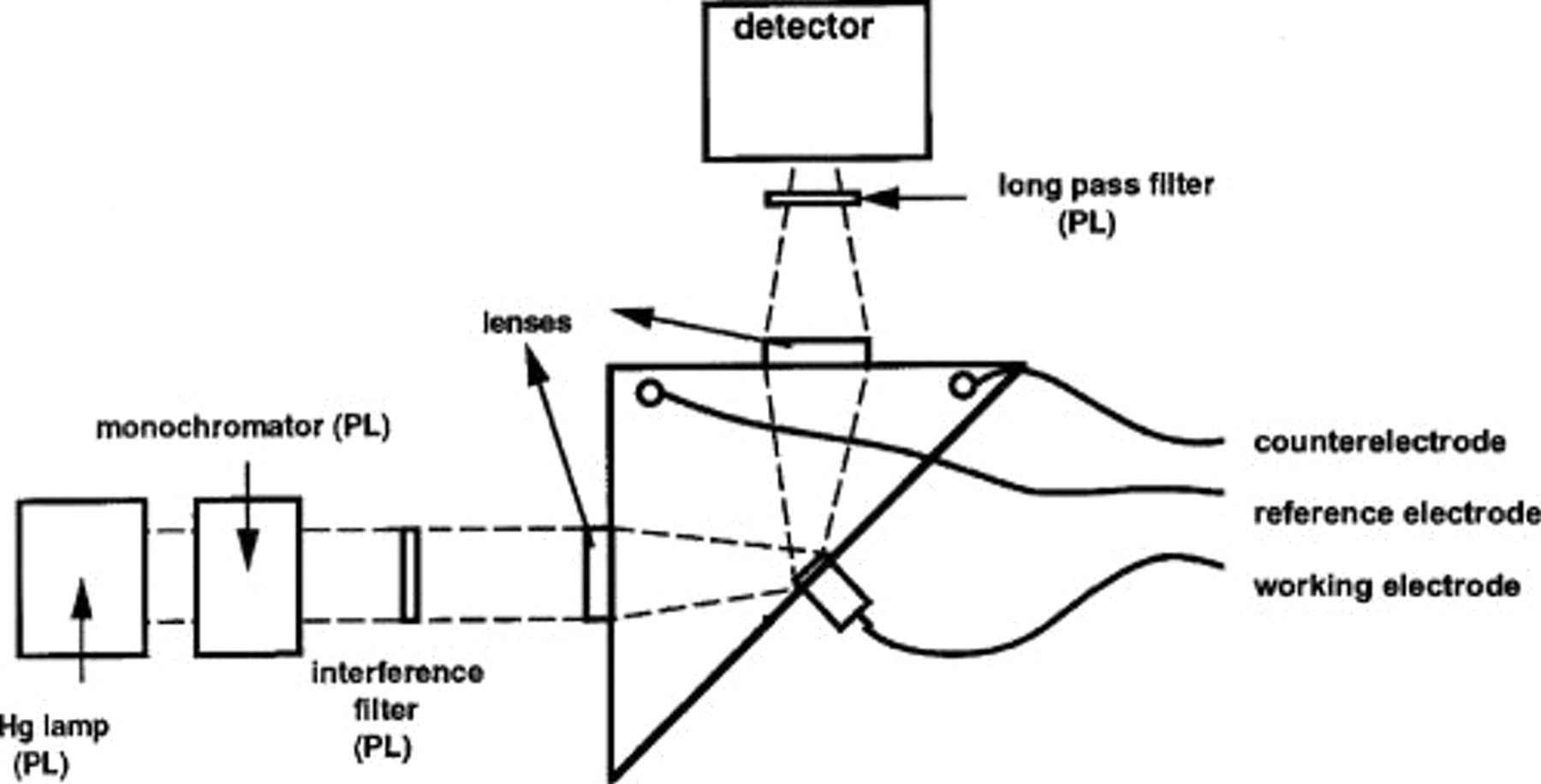
Figure 1. Top view of the experimental setup for the luminescence measurements
For n- electrodes, the luminescence experiments were performed on so-called new electrodes, which were only subjected to a 6 M HCl dip for 30 s, and on so-called etched electrodes, which were photoanodically etched in 1 M
  at
at  vs SCE5 prior to the HCl dip. For n-
 electrodes, the experiments were only performed upon new electrodes.
Results
Photoluminescence measurements at n-
 electrodes

PL spectra were recorded at n- electrodes in 1 M
  for different values of the electrode potential and different excitation intensities. A broad luminescence band in the yellow spectral region was observed (see Fig. 2). No shift of the peak maximum position with changing electrode potential or changing excitation intensity was observed. The PL spectra could be fitted very well using a Gaussian-shaped band with a peak maximum at 2.20 eV and a full width at half maximum (fwhm) value of 0.55 eV. The PL intensity
  at the peak maximum is represented in Fig. 3 as a function of the electrode potential. The PL intensity increases when the potential becomes more negative and reaches a more or less limiting value
  at
at  vs SCE. When
  is plotted vs the depletion layer width
  , linear plots are obtained for
  , with a positive intercept on the ordinate axis (see insert Fig. 3). PL measurements at n-
 electrodes were already described thoroughly in Ref. 4. As shown in Fig. 2, the PL spectra at n-
 and n-
 electrodes are identical. Also the relationship between
  and the electrode potential is similar for n-
 electrodes and n-
 electrodes.
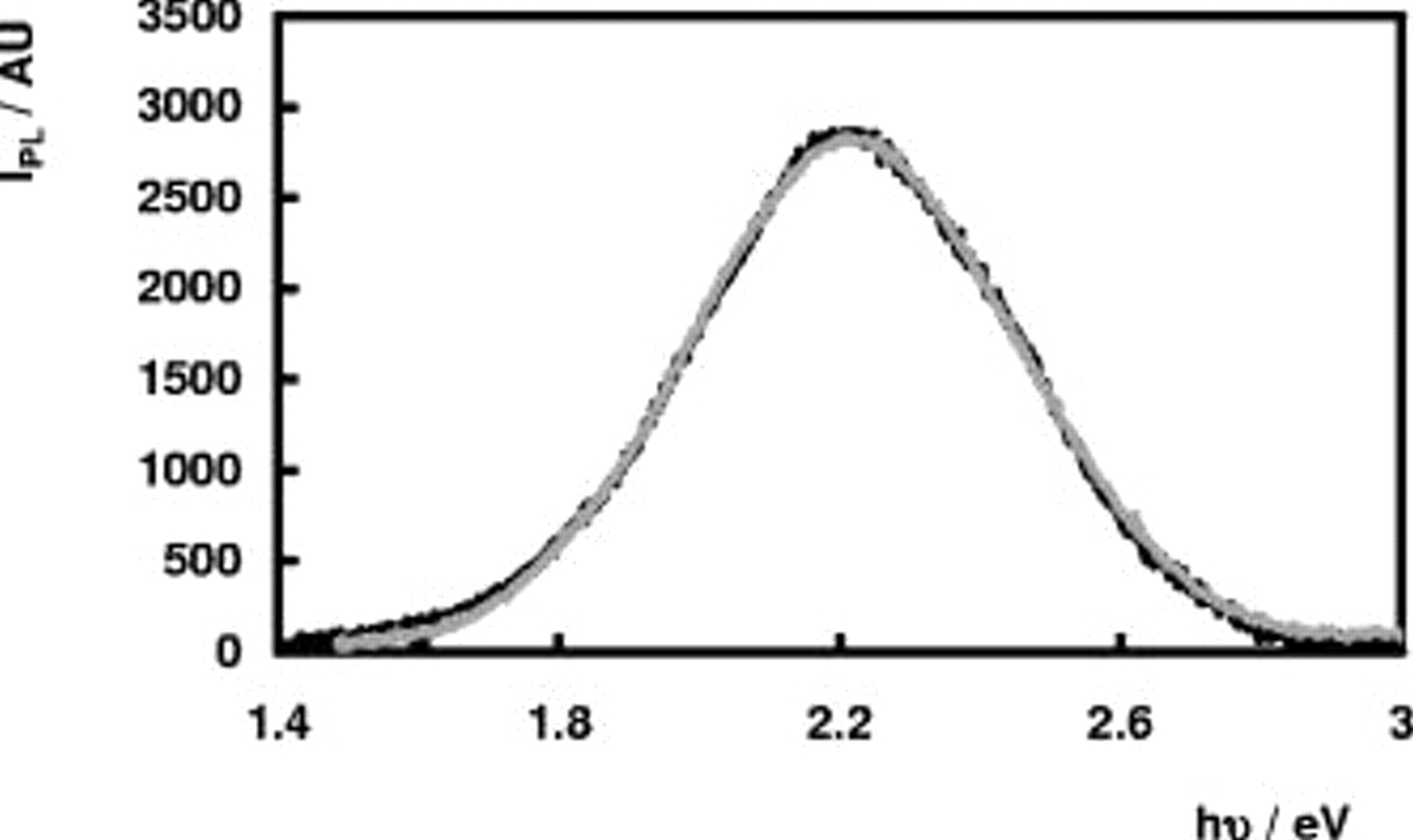
Figure 2. PL spectra in 1 M  at
at  vs SCE (normalized intensities): (—) (black) at an n-
 electrode and (—) (gray) at an n-
 electrode.
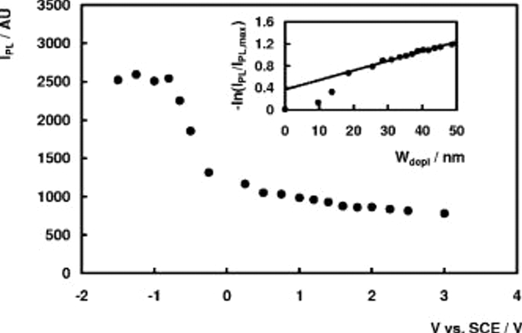
Figure 3. PL intensity as a function of the electrode potential at a n- electrode in 1 M
  . Inset:
  vs
vs  .
.
Electroluminescence measurements at electrodes

EL spectra were recorded at new n- electrodes and at new and etched n-
 electrodes, as a function of the electrode potential, in solutions containing 0.05 M persulfate ions (pH 4). These measurements were performed at different samples. For each sample, the potential dependence of the EL spectra was measured several times. The variation of the electrode potential was always at random. The intensity of spectra recorded at a fixed value of the electrode potential showed some irreproducibility. This may at least partially be due to the instability of the system. At a constant value of the electrode potential, the current associated with the reduction of persulfate ions may show some time evolution.
n-

EL is observed at values of the electrode potential  vs SCE. Figure 4 shows EL spectra at two different values of
  . For values of the electrode potential more negative than about
  vs SCE, the EL is located in the yellow spectral region, and the peak maximum position and fwhm value of the spectra are close to those observed for the PL band. For
  vs SCE
  vs SCE, however, an additional reddish component is observed in the EL spectra, besides the yellow band at 2.20 eV (shown by the gray curve in Fig. 4). This observation is also visible to the naked eye. When the electrode potential is changed from
  vs SCE to
  vs SCE, the luminescence clearly changes from reddish to yellow. Because shoulders are visible in the low-energy part of the spectrum recorded at
  vs SCE, the reddish luminescence appears to be a superposition of a number of different bands. The reddish component of the spectra was deconvoluted using Gaussian bands centered at
 ,
, 
 , and
, and  . In the higher energy part of the spectra, the yellow luminescence band observed in the PL experiments (2.20 eV;
  ) did not always fit the experimental spectra satisfactorily; for some values of
  , features at about 2.30 and 2.55 eV could be observed in the EL spectra. An example of a spectral deconvolution for n-
 electrodes is shown in Fig. 5.
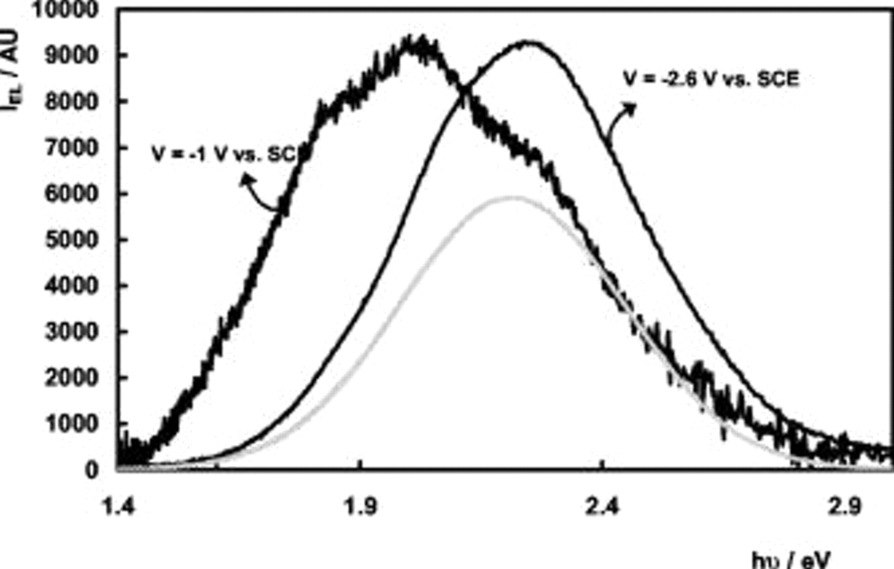
Figure 4. EL spectra in 0.05 M  (pH 4) for two values of the electrode potential
  at an n-
 electrode (normalized intensities): (—) (gray) Gaussian band at 2.20 eV.
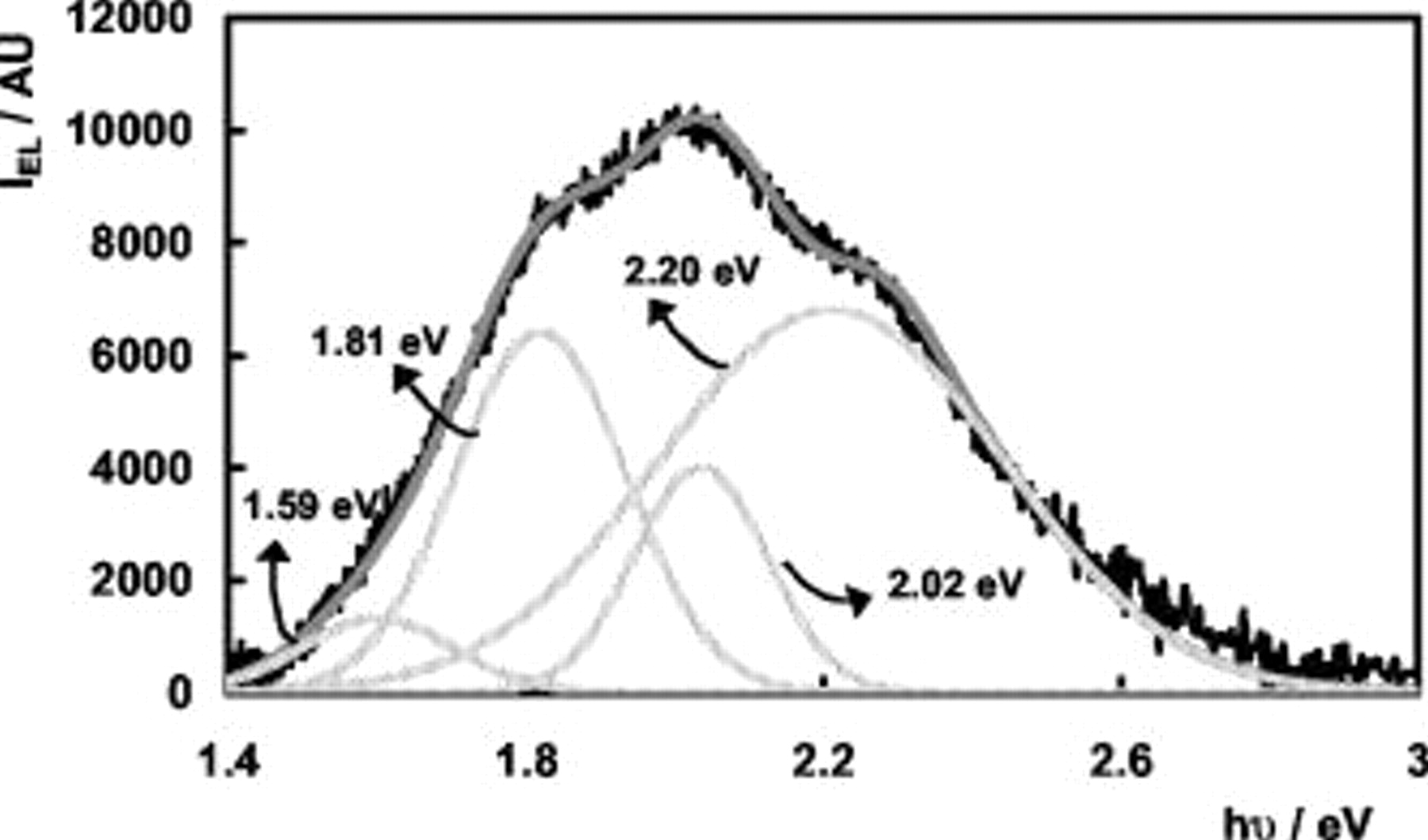
Figure 5. Deconvolution of EL spectrum at an n- electrode in 0.05 M
  (pH 4),
  vs SCE: (—) (black) experimental spectrum; (—) (light gray) theoretical Gaussian bands; and (—) (dark gray) total fit.
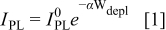
Figure 6 shows the intensity of the bands at 2.20, 2.02, and 1.81 eV as a function of the electrode potential. The EL intensity of the 1.59-eV band as a function of  shows the same evolution as the 2.02- and 1.81-eV bands but with lower intensity not shown in the figure. The features at 2.30 and 2.55 eV only show a weak potential dependence. Moreover, their intensities appear to be sample-dependent and these bands were not investigated in further detail. From Fig. 6 it follows that the intensities of the 1.59-, 1.81-, and 2.02-eV bands go through a maximum, whereas the intensity of the 2.20-eV band goes through a maximum, after which it increases steeply.
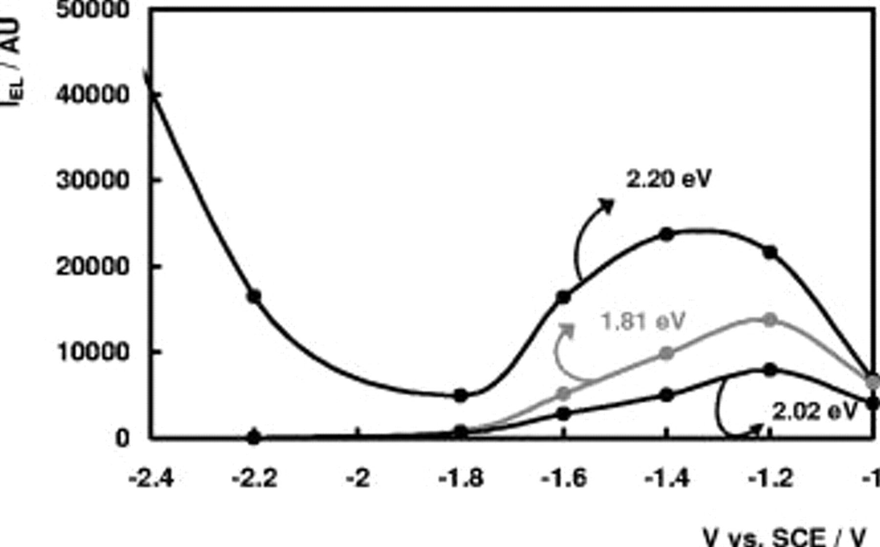
Figure 6. EL intensity of the 1.81-eV band, 2.02-eV band, and 2.20-eV band at a n- electrode in 0.05 M
  (pH 4) as a function of
  .
.
n-
Figure 7A and 7B shows experimental EL spectra as well as theoretical fits for spectra recorded at new and etched n- electrodes, respectively. As for the n-
 electrodes, the spectral distribution of the EL depends upon the electrode potential. For very negative values of the electrode potential (more negative than
  vs SCE for new electrodes and more negative than
  vs SCE for etched electrodes), the EL is located in the yellow spectral region whereas for more positive values of the electrode potential, additional red luminescence shows up in the spectra. Although no clear shoulders are present in the EL spectra for n-
 electrodes, the red luminescence for n-
 electrodes was fitted with three bands located at 1.59, 1.81, and 2.02 eV, in analogy to the EL spectra at n-
 electrodes (but with larger fwhm values than for the n-
 measurements). It has to be remarked, however, that the red luminescence for n-
 could equally be fitted using a single broad band centered at 1.9 eV (see Ref. 4). In the higher energy part of the spectra a band at about 2.55 eV was in some cases needed to obtain satisfying fits of the experimental spectra, as was also the case for the n-
 electrodes.
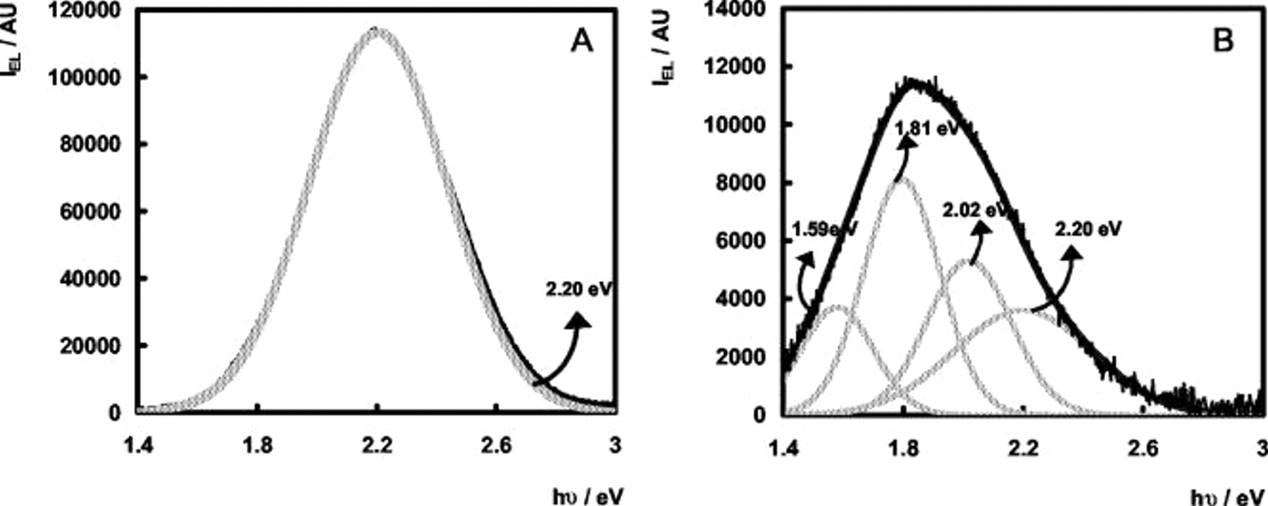
Figure 7. Deconvolution of EL spectrum at n- electrodes in 0.05 M
  (pH 4): (—) (black) experimental spectrum, (—) (light gray) theoretical Gaussian bands, and (—) (dark gray) total fit. (A) New electrode;
  vs SCE. (B) Etched electrode;
  vs SCE.
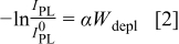
Figures 8 and 9 show the intensity of the bands at 2.20, 2.02, and at 1.81 eV as a function of the electrode potential for new and etched n- electrodes, respectively. As for the n-
 electrodes, the EL intensity of the 1.59-eV band is not shown in the figures as it shows the same evolution as the 2.02- and 1.81-eV bands but with lower intensity. The band at 2.55 eV was not investigated in more detail, for the same reasons as mentioned in the section on n-
 electrodes.
Discussion
Photoluminescence measurements
Under photoexcitation, a yellow defect luminescence band centered at 2.20 eV  is observed which is identical for both n-
 as well as for n-
 electrodes. This indicates that the same defect level is present in both types of material. The yellow luminescence band is commonly observed for n-GaN (mostly centered between 2.15 and 2.25 eV), independent of the growth technique or doping. The type of transition responsible for this band has been an object of research for many years. Most often it is assumed that it is due to a transition from a shallow donor to a deep acceptor. The potential dependence of
  for n-
 electrodes was analyzed on the basis of a model for the PL intensity originally developed by Gärtner for Schottky diodes.6 Later, more extended versions of this model were described for semiconductor/electrolyte interfaces, e.g., by Smandek et al.7 According to the most commonly used version of the Gärtner model for semiconductor/electrolyte interfaces, the depletion layer of an n-type semiconductor acts as an infinite sink for holes. It is assumed that all holes which are either generated inside the depletion layer or which are able to reach the edge of the depletion layer by diffusion from the bulk are swept toward the surface very fast, where they disappear immediately due to nonradiative surface reactions (i.e., zero hole concentration at the edge of the depletion layer as well as inside the depletion layer). As a consequence, these holes are lost for luminescence. Because for n-type semiconductors the depletion layer becomes wider when the electrode potential is made more positive, the luminescence signal should decrease with more positive potential. Mathematically, the following relationship between the PL intensity under depletion conditions
  and the depletion layer width
  is predicted
or
In Eq. 1, 2,  is the luminescence intensity at
  (i.e., at flatband potential) under the boundary conditions analogous to those set to describe the PL intensity under depletion conditions. The measured luminescence signal at flatband only equals
  if the holes which reach the electrode surface by diffusion disappear due to nonradiative surface reactions as soon as they reach the surface (i.e., zero hole concentration at the electrode surface).
As can be seen from Fig. 3, the luminescence intensity reaches a more or less limiting value  at
at  vs SCE. This value of
  vs SCE is very close to the value of the flatband potential for n-GaN electrodes in 1 M
  solutions,5 which appears to be in agreement with the simple model presented above.
From the inset of Fig. 3, it follows that a linear relationship is observed between  and
and  for
for  , i.e., for reasonably large positive potentials. As argued by Smandek et al. ,7 the conditions set in the Gärtner model are most probably met in this potential range so the luminescence intensity is then given by Eq. 1, in agreement with the experimental results [linear relationship between
  and
and  ]. From the slope of this plot, a value for the absorption coefficient α of about
  was calculated, in good agreement with literature values8 of α for comparable values of the photon energy (about
  at
at  ).
).
However, when the PL intensity under depletion conditions is described by Eq. 1, the experimentally measured PL intensity at flatband  cannot be equal to
  . According to Eq. 2 a plot of
  vs
vs  should then be linear with a zero intercept on the ordinate axis. From the insert of Fig. 3 it can be seen that the intercept is clearly larger than zero, which indicates that the real luminescence intensity at flatband potential is larger than
  . As discussed in Ref. 4, a value for the PL intensity at flatband conditions larger than
  does not affect the slope (i.e., the value for α) but leads to a positive intercept on the ordinate axis in a [
 vs
vs  ] plot. A possible explanation for the fact that
  is larger than
  is that at
  , the conditions set in the Gärtner model are not fulfilled. Perhaps at flatband situation holes do not react infinitely fast via nonradiative reactions at the surface so that a steady-state concentration of holes exists at or near the electrode surface, leading to an increased luminescence signal. Another possible explanation is enhanced yellow luminescence in the near-surface region. At
  , the luminescence partially originates from the near-surface region (or possibly even the surface itself), whereas at high reverse bias this near-surface region acts as a "dead layer". If then the near-surface region possesses a higher concentration of recombination levels responsible for the yellow luminescence,
  around flatband potential can be significantly higher than predicted by the Gärtner model. Several literature reports exist in which it is also suggested that the yellow luminescence intensity of n-GaN samples is higher in the near-surface region as compared to the bulk region or that the yellow luminescence of n-GaN possesses a significant contribution of the semiconductor surface itself.9, 10 Surface recombination is generally assumed to occur nonradiatively. In the case of n-
 , however, reports on radiative surface recombination exist.11, 12 This has been attributed to the wide bandgap of this semiconductor, leading to a relatively large energetic spacing between different surface levels.13 The same argument may hold for GaN.
Electroluminescence measurements
Cathodic EL is observed during the reduction of persulfate ions. This effect can be ascribed to radiative recombination of electrons and holes, the latter being injected by  radicals which are formed by reaction between persulfate and conduction band electrons.
For both n- electrodes and n-
 electrodes (new and etched), the spectral distribution of the EL depends strongly upon the electrode potential. This appears to be because the spectra consist of different bands, the intensities of which show a different potential dependence (see Fig. 6, 8 and 9). The influence of the electrode potential on the spectral distribution is most probably a bandbending effect. Because for EL the holes are injected from the solution side of the interface whereas for PL the zone of hole creation is determined by the penetration depth of the photons (about 100 nm for the photon energy used in this work), EL is generally situated closer to the electrode surface than PL. Under depletion conditions, the injected holes remain close to the surface, whereas at more negative potentials, the holes are drawn more efficiently into the interior of the semiconductor. The bands at 1.59, 1.81, and 2.02 eV are only observed in the potential region around flatband potential (
 vs SCE at pH 4 for new electrodes; about 100–200 mV more positive for etched electrodes14). In this potential region it can be assumed that holes are present only at or near the electrode surface so that these bands may be ascribed to radiative recombination via (near-) surface states. Because these bands are not at all visible in the PL spectra, the (near-) surface region from which they originate must be restricted to a small distance from the surface.
In our previous paper on galvanostatic EL measurements at n- electrodes,4 we observed almost no dependence of the spectral distribution on the electrode potential for electrodes that were not etched, contrary to the potentiostatically obtained results presented in this paper. Different effects may account for these apparent contradictions. First, the "measuring window" is not the same for both types of experiments. The sensitivity of the potentiostatic experiments presented in this paper is larger than that of the galvanostatic experiments in Ref. 4. Moreover, it was already mentioned that the n-
 system is not very stable. As it is the electrode potential and not the cathodic current density has the largest influence on the spectra; a drifting electrode potential poses a more serious problem regarding the accuracy of the results than a drifting cathodic current density. Finally, as the samples in this work were cut from different wafers than those used in Ref. 4, some sample dependence may also play a role. We indeed observed some quantitative differences in the exact
  vs
vs  relationship for the different bands from one sample to another. This is not surprising. The exact spectral distribution at a certain value of the electrode potential is sensitive to a variety of parameters (e.g., the position of the flatband potential, the exact current density–voltage behavior, and the concentration of the defect states responsible for each band), all of which may be somewhat sample-dependent.
EL measurements at n-GaN electrodes in aqueous persulfate solutions were also performed by Hung et al.2 They observed a shift of the peak maximum position of the EL spectra from 2.0 eV toward 2.15 eV when the electrode potential was changed from  vs SCE to
  vs SCE, which may agree qualitatively with the results presented in this paper.
Although the yellow luminescence (YL) is the most commonly reported defect PL band reported for n-GaN, reports also exist on red PL at n-GaN, mostly at material grown by hydide vapor phase epitaxy (HVPE) and molecular beam epitaxy (MBE).15 As discussed by Reuter et al. ,16 red luminescence is often weak and difficult to observe in GaN that has very strong YL. As it has been found that YL is generally far more intense in GaN grown by MOCVD than in GaN grown by HVPE, this may explain why red luminescence is generally not observed in MOCVD-grown GaN. Recently, PL measurements on n-GaN nanocrystallites [average size about 10 nm determined from X-ray diffraction measurements; larger aggregates of about 20–100 nm were observed by transmission electron microscopy (TEM)] were performed and the spectra were characterized by a broad luminescence band centered at 1.9 eV.17
The choice to fit the red luminescence at n- electrodes with the same bands as the EL spectra at n-
 electrodes implies that we believe the same radiative (near) surface centers may be present in both n-
 and n-
 . It is not easy to speculate on the origin of these (near) surface states. Because the emission energy of these (near) surface recombination processes is not very different from the well-known 2.2-eV emission, the (near) surface states involved may be related to the same defect (most probably triply negatively charged Ga vacancies or complexes of these vacancies with oxygen). They may simply have a different energy because their surrounding at/near the surface is different from that in the bulk. A somewhat analogous explanation has been given for the red PL of n-GaN in the literature. It has been suggested that the point defect responsible for the YL may produce emission similar to the YL but shifted in energy (toward red) if this point defect is trapped by extended defects.15
Luminescence at 2.20 eV originates from the bulk of the semiconductor, as also became clear from the PL experiments. However, the evolution of the intensity of the 2.20-eV band as a function of the electrode potential may suggest that the concentration of defect levels responsible for this band is higher at the (near-) electrode surface as compared to the bulk material, because a peak is observed before the steep increase of the intensity of this band. Enhanced yellow emission in the near-surface region as compared to the bulk, or even emission from the surface itself, is in agreement with some literature reports for the YL at n-GaN9, 10 and may also explain why the value of  at flatband conditions is larger than that expected from an extrapolation of
  under depletion conditions, as discussed before. For n-GaAs, a peak followed by a steep increase in the
  vs
vs  relation has also been found when scanning from more positive to more negative potentials.18 This was explained by a transition of the surface from a stable oxidized to a stable reduced surface when going from anodic to cathodic potentials. During this transformation, surface states are formed which act as efficient, nonradiative recombination centers and luminescence is quenched. If the surface is stabilized again at the most negative potentials, these recombination centers disappear and the EL intensity increases again. Although we cannot exclude an analogous explanation for our results, we believe that an enhanced emission in the near-surface region as compared to the bulk may equally explain the behavior observed.
At n- electrodes, EL measurements show some quantitative differences between new and etched electodes. When comparing Fig. 8 to Fig. 9, it can be seen that at the same amount of bandbending (taking into account the positive shift of
  between 100 and 200 mV due to photoanodic etching14), the relative intensities of the 1.59-, 1.81-, and 2.02-eV bands as compared to the intensity of the 2.20-eV band are much larger. A detailed interpretation for this effect cannot easily be given, as we do not know the exact spatal origin of all bands. Photoanodic etching may increase the concentration of the defects, responsible for the 1.59-, 1.81-, and 2.02-eV, band, relative to the concentration of the defect responsible for the 2.20-eV band. A decrease of nonradiative surface recombination due to etching may also play a role, if, for example, luminescence at 1.59, 1.81, and 2.02 eV originates from the surface itself and luminescence at 2.20 eV occurs at the near surface but not at the surface itself.
Figure 8. EL intensity of the 1.81-eV band, 2.02-eV band, and 2.20-eV band at a new n- electrode in 0.05 M
  (pH 4) as a function of
  .
.
Figure 9. EL intensity of the 1.81-eV band, 2.02-eV band, and 2.20-eV band at an etched n- electrode in 0.05 M
  (pH 4) as a function of
  .
.
Conclusions
In this paper, a comparative study was performed on the PL and EL behavior of n-GaN electrodes grown on sapphire and n-GaN electrodes grown on Si.
PL measurements were performed at n- electrodes in acidic solutions. The well-known YL band was observed at 2.20-eV. This PL band was identical to the one at n-
 electrodes, showing that the same defect level is present in both n-
 and n-
 electrodes. The potential dependence of the PL intensity was analyzed according to a simple model originally developed by Gärtner. Deviations from this model may be explained by assuming that the 2.20 eV luminescence is enhanced in the near-surface region as compared to the semiconductor bulk.
When holes were injected into an n-GaN electrode by a  radical, EL was observed. The spectral distribution showed a complex dependence on the electrode potential. It was demonstrated that this is because the spectra consist of different bands, the intensity of which show a different potential dependence, presumably due to their different spatial origin. Besides the 2.20-eV band, bands at 1.59, 1.81, and 2.02 eV were observed. The latter were only observed around flatband potential, indicating that they originate from recombination via energy levels which are only present at or near the electrode surface. As the EL behavior was qualitatively similar for n-
 and n-
 electrodes, this suggests that the same (near) surface states are present in both types of material. Photoanodic etching was found to enhance luminescence at 1.59, 1.81, and 2.02 eV relative to luminescence at 2.20 eV.
In general, these results show that measuring luminescence properties in solution as a function of the electrode potential may yield useful information concerning spatial variations in the occurrence and efficiency of radiative processes.
Ghent University assisted in meeting the publication costs of this article.