
Abstract
Both Ga-based (GaAs, AlGaAs) and In-based (InGaP, InP, InAs, and InGaAsP) compound semiconductors were etched in a planar inductively coupled plasma (ICP) reactor in pure  The Ga-based materials etched at significantly higher rates, as expected from the higher volatilities of their trichloride etch products relative to
  In contrast to the more common cylindrical geometry ICP sources, the dc self-bias which controls ion energy is not strongly dependent on source power up to ∼400 W while etch rates increase rapidly over this power range. The source tunes easily even at very low powers (<100 W) but operates inefficiently above ∼10 mTorr, with a marked decrease in both emission intensity from the discharge and in resulting etch rates of the compound semiconductors. The etched surfaces of both AlGaAs and GaAs have comparable root-mean-square roughness and similar stoichiometry to the unetched control samples, while the surfaces of In-based materials are degraded by the
  etching. © 2004 The Electrochemical Society. All rights reserved.
Export citation and abstract BibTeX RIS
The GaAs/AlGaAs and InP/InGaAsP heterostructures are the basis of most modern compound semiconductor electronic and photonic devices.1 2 3 4 5 In particular, devices such as high electron mobility transistors (HEMTs) and heterojunction bipolar transistors (HBTs) rely on the ability to selectively etch one component of the heterostructure over the other in applications such as microwave power amplifiers and low noise amplifiers.6 7 8 9 10 11 12 13 14 15 16 17 18 19 20 21 22 23 24 25 26 27 28 Further requirements for this etching are vertical sidewalls and minimal surface disruption. The latter involves both the lattice damage created by ion bombardment and any changes in stoichiometry. High density plasmas have proven attractive for these applications, with the ability to control both ion density and ion energy.8 9 10 11 12 13 A key point that emerged from past studies with both electron cyclotron resonance (ECR) and cylindrical geometry inductively coupled plasma (ICP) etching of these heterostructures is that significant damage can be created even at moderate source powers (300-500 W),12 16 18 so it is essential to develop high density sources that can operate efficiently over a broad range of powers and be usable over a continuous range of conditions. Our initial experience with planar ICP sources is that they are continuously tunable at low powers (0-200 W) and therefore offer a versatile range of operating conditions for applications from through-wafer vias to low damage mesa formation.
In this paper we describe the results of etching GaAs, AlGaAs, InP, InGaP, InAs, and InGaAsP in a planar ICP tool with a single  chemistry. The system appears well suited to patterning of GaAs/AlGaAs at room temperature, producing clean, vertical profiles.
Experimental
GaAs, InP, and InAs wafers were cut from Czochralski-grown boules and were nominally undoped with (100) orientation in all cases. The  and
and  were grown lattice-matched to GaAs substrates by either metalorganic molecular beam epitaxy (MOMBE) or metalorganic chemical vapor deposition (MOCVD), respectively. The layers were 2 μm thick and were nominally undoped. The InGaAsP
  was grown lattice-matched to InP substrates by MOMBE. These layers were a 1 μm thick and were also undoped.
Etching was performed in a Cliotek, Inc., planar ICP system, with the radio-frequency (rf) chuck power (13.56 MHz) varied from 0 to 150 W and the ICP source power (also 13.56 MHz) varied from 0 to 500 W. Samples were patterned with 1 μm thick photoresist and mounted on an anodized Al carrier wafer with vacuum heat sink paste. The Al carrier was clamped to the electrode during processing, maintaining a sample temperature of ∼25°C. The total  gas flow was 20 standard cubic centimeters per minute (sccm), entered through an electronic mass flow controller. Etch depth was measured by stylus profilometry, while scanning electron microscopy (SEM) and atomic force microscopy (AFM) were used to examine etch anisotropy and surface roughness. X-ray photoelectron spectroscopy (XPS) was used to measure near-surface composition.
Results and Discussion
Figure 1 shows the etch rates of the Ga-based and In-based materials as a function of ICP source power for fixed chuck power (100 W) and process pressure (7.5 mTorr). Note that GaAs and AlGaAs etch at practical rates even without any enhancement of the discharge by applying source power. This is a result of the relatively high volatility of the 
 and
and  etch products. By sharp contrast, InGaP shows negligible etch rate below 100 W source power as do the other In-based materials. As is well known,
  is relatively involatile and requires either an elevated process temperature (>130°C) or very high ion flux to enhance its desorption from a chlorinated surface. The involatility of
  leads to very rough surfaces on all In-based materials after etching. For example, after etching only 600 Å of InP, the root mean square (rms) roughness measured by AFM was 18.4 Å while the unetched control exhibited an rms roughness of 1.8 Å. The surface also was covered with In droplets, topped with a chlorinated residue. By contrast, after etching ∼1.5 μm of GaAs on AlGaAs, the rms roughness was 5.7 Å, only slightly rougher than the unetched control values of 3-4 Å.
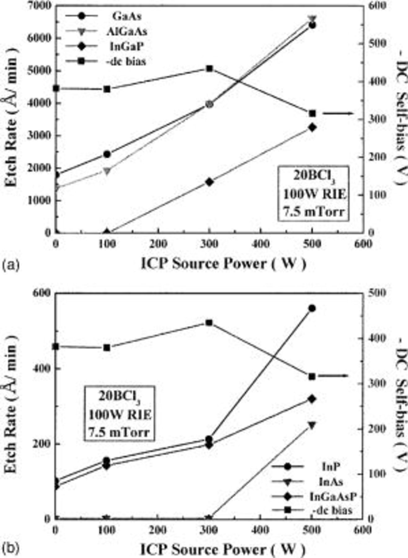
Figure 1. Etch rate of (a) GaAs, AlGaAs, and InGaP and (b) InP, InAs, and InGaAsP as a function of ICP source power in  discharges (7.5 mTorr, 100 W rf chuck power).
Figure 2 shows optical emission spectra as a function of both source power and process pressure. There is little enhancement of plasma emission intensity for source powers ⩽100 W and the emission is significantly quenched at a pressure of ∼15 mTorr. The broad continuum from 400-800 nm is due to molecular excitation of the 
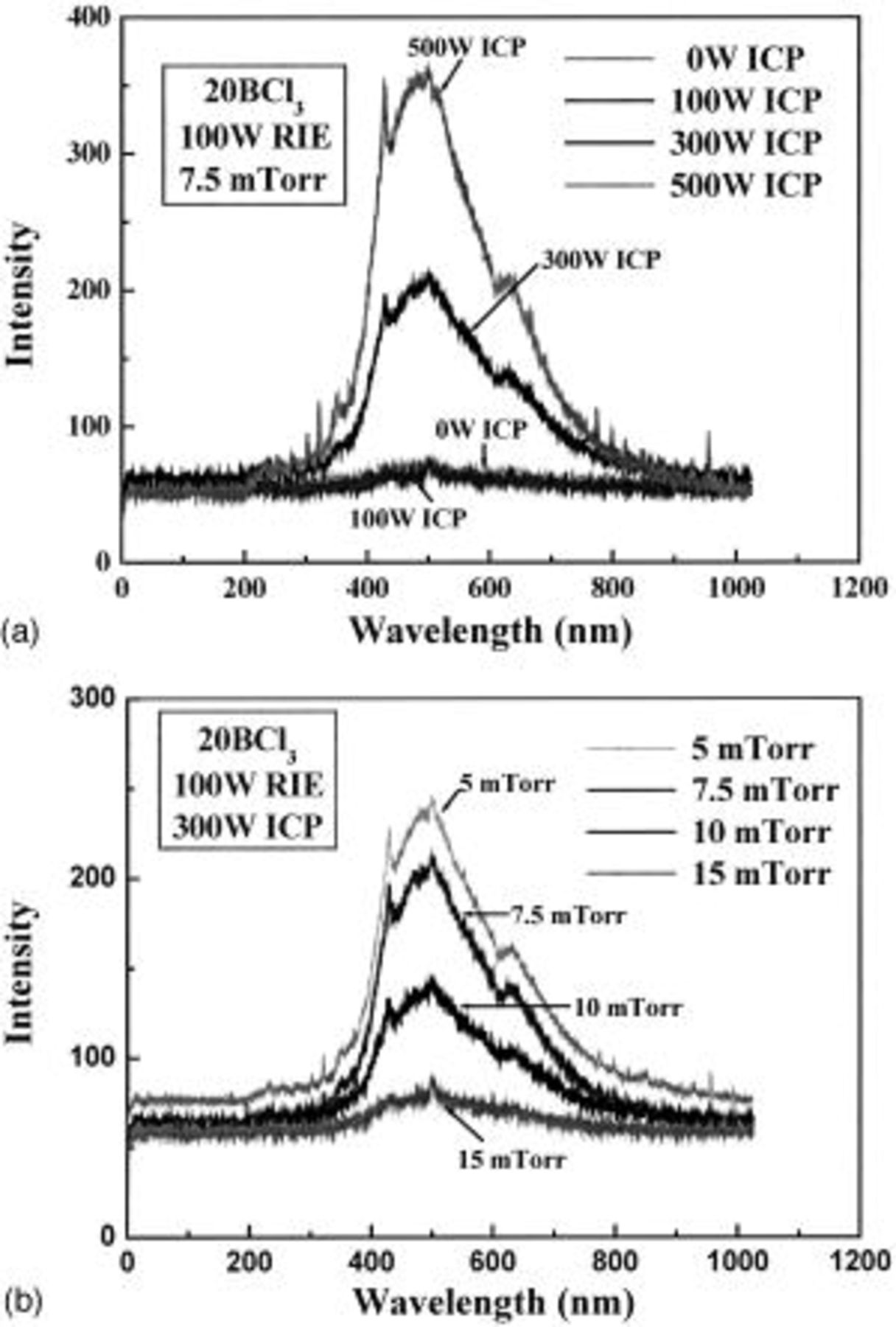
Figure 2. Optical emission spectra from  discharges as a function of (a) ICP source power or (b) process pressure.
Figure 3 shows the material etch rates as a function of chuck power. Once again, the etch rates for GaAs and AlGaAs are identical within the experimental error. This proves that there is no significant incubation time for onset of the AlGaAs etching and that the  is effective in removing the native oxide on the material. The selectivity of etching GaAs and AlGaAs over photoresist was >3:1 under all conditions examined. The etch rates for all materials increased with increasing rf chuck power, but once again the rates were much lower for the In-based semiconductors. The etch rates for GaAs and AlGaAs are ∼3000 Å/min even at low dc self-biases (<−75 V) which are conditions desirable for low damage device etching.
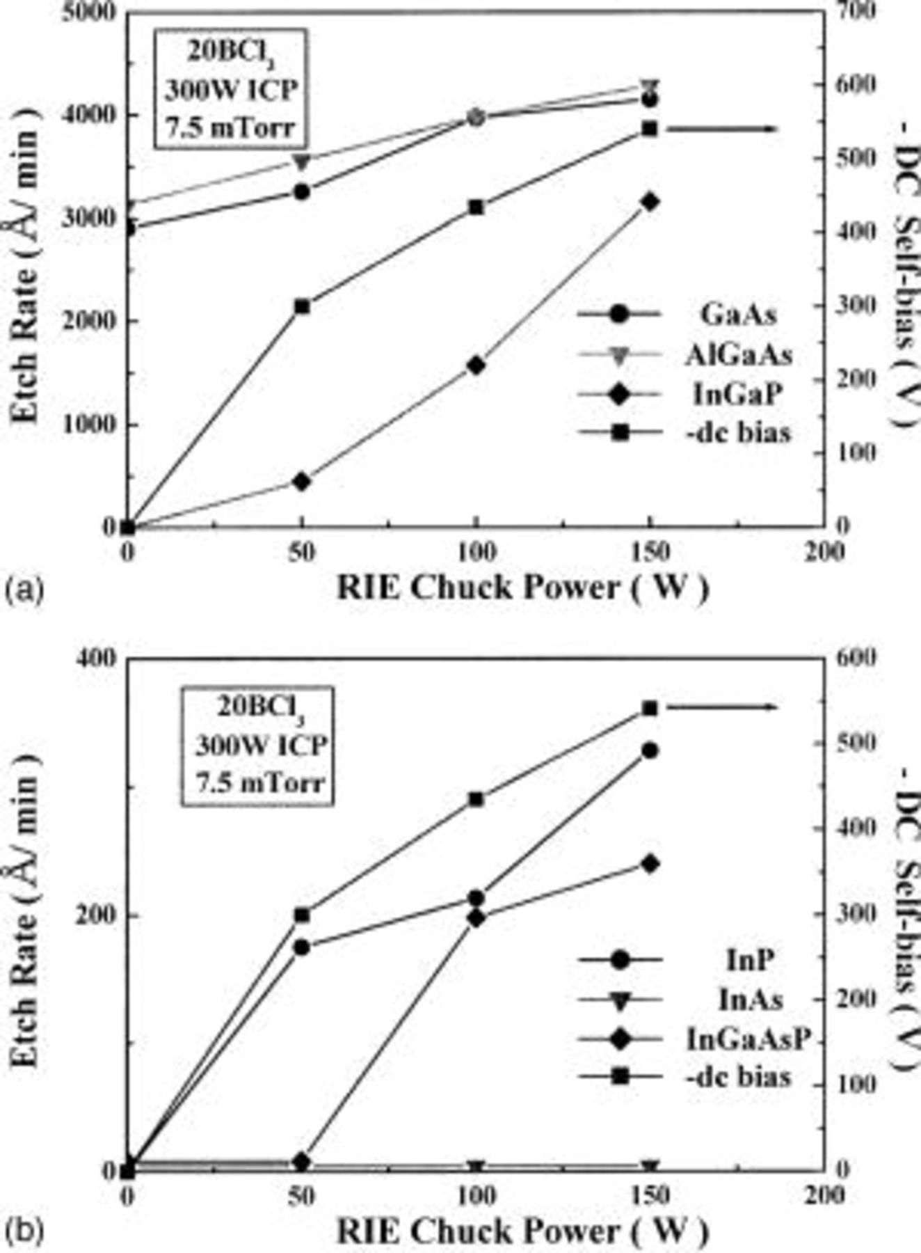
Figure 3. Etch rate of (a) GaAs, AlGaAs, and InGaP and (b) InP, InAs, and InGaAsP as a function of rf chuck power in  discharges (7.5 mTorr, 300 W source power).
As was evident from the optical emission spectra (OES) data, the ion density in the discharge falls off rapidly with increasing process pressure. Figure 4 shows that this correlates well with decreasing etch rates for all the semiconductors because all III-V etching is ion-assisted to some extent. The In-based materials basically do not etch at process pressure ⩾10 mTorr, even though the self-bias is still ⩾−300 W. At these pressures the buildup of an  selvedge layer outweighs the ion-assisted desorption of the etch product.
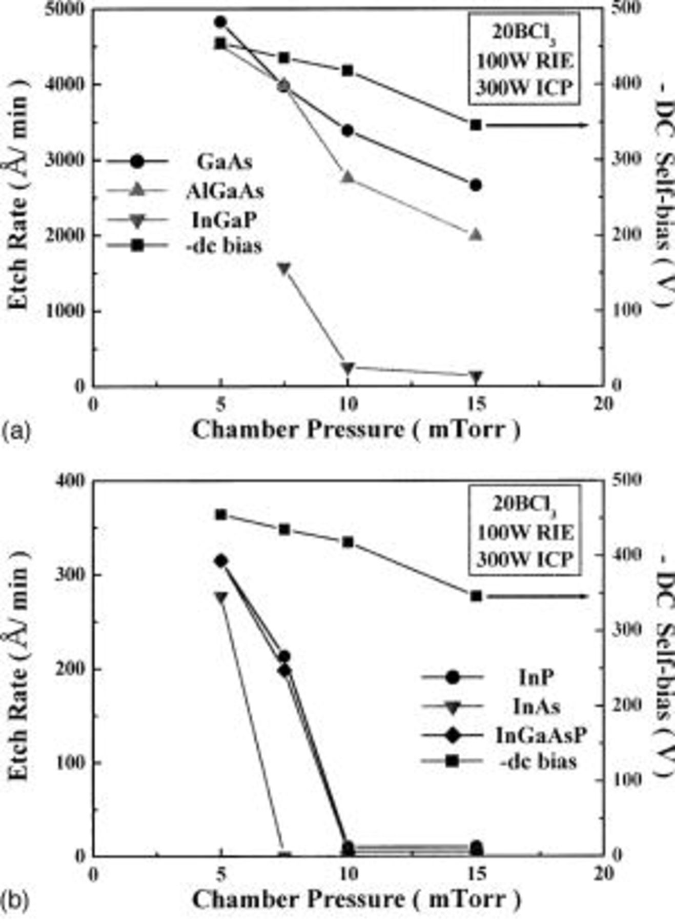
Figure 4. Etch rate of (a) GaAs, AlGaAs, and InGaP and (b) InP, InAs, and InGaAsP as a function of process pressure in  discharge (100 W chuck power, 300 W source power).
Figure 5 shows excellent anisotropy of etched features in GaAs and the smooth surface of the etched region. Similar results were achieved for AlGaAs. The anisotropy is at least partially a result of a passivation of the sidewall of the etched features by redeposition of resist by-products, since there was more significant undercut when  masks were used under the same set of process conditions. The bottom of Fig. 5 shows XPS spectra of the GaAs before and after
  etching (100 W chuck power, 300 W source power). The etched surface returns the same stoichiometry as for the unetched control, indicating that the Ga and As etch products are removed at equal rates. No B- or Cl-related residues could be detected at the surface.
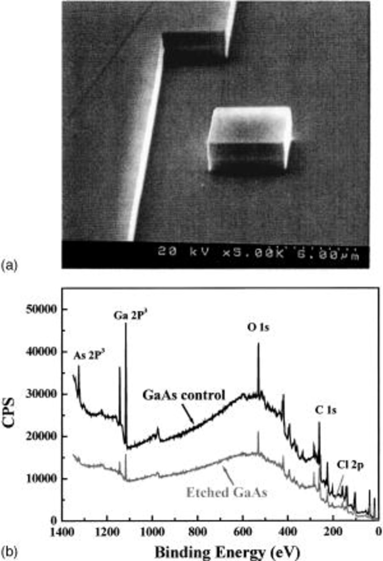
Figure 5. (a) SEM micrograph of feature etched into GaAs using a 3 min process in a  discharge (7.5 mTorr, 100 W chuck power, 300 W source power). The resist mask is still in place. (b) XPS spectra of GaAs surface before and after the same etch.
SEM micrographs of AlGaAs and InGaP etched under the same conditions are shown in Fig. 6. The AlGaAs shows similar excellent anisotropy and smooth surfaces as for GaAs. By contrast, the InGaP surface is somewhat rougher and there are trenches at the edge of the etched features. After etching to a depth of 0.47 μm, the rms roughness of the InGaP surface was ∼20 Å compared to a value of 3.1 Å on the unetched control material.
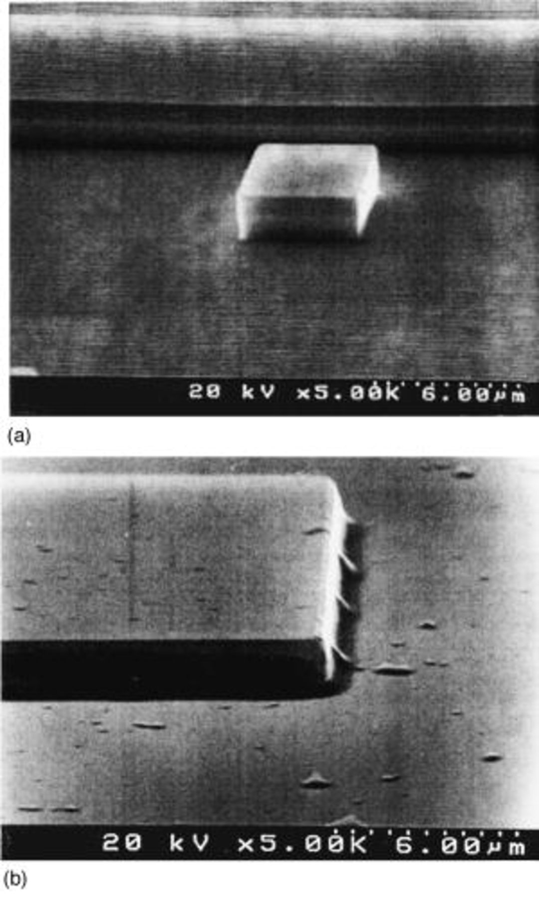
Figure 6. SEM micrographs of features etched into (a) AlGaAs or (b) InGaP during a 3 min process in a  discharge (7.5 mTorr, 100 W chuck power, 300 W source power). The resist mask is still in place in both cases.
Two features of the planar ICP reactor relative to more conventional cylindrical geometry were noteworthy. First, the planar source remained in a predominantly capacitively-coupled mode at low source powers (100 W), as evidenced by the minimal dependence of dc self-bias on source power. This is a region of interest for high selectivity, low damage etching of GaAs/AlGaAs heterostructures in applications such as mesa etching of HEMTs and HBTs. Second, the planar source may be ignited both with and without rf chuck power, which is generally not the case with cylindrical geometry ICP sources. This latter quality widens the range of potential applications of the reactor to include dry surface cleaning or selective film removal in addition to the usual anisotropic etch processes.
Conclusions
A plasma geometry ICP source was found to provide smooth, anisotropic pattern transfer of photoresist-masked GaAs and AlGaAs at practical rates in  discharges. The etch rates for In-containing III-V semiconductors was much lower under the same conditions due to the low volatility of the
  etch product. The planar ICP appears to have the same advantages over most cylindrical sources in terms of operation at low source and chuck powers, a region of great interest for low damage processing of devices.
Acknowledgments
The authors appreciate technical support from D. J. Jung and K. S. Cho at Cliotek, Inc. in Korea. The work at Inje University was supported by Korea Science Foundation grant R05-2002-000013680-2003. The work at University of Florida is partially supported by NSF CTS-1109973.
The University of Florida assisted in meeting the publication costs of this article.