
Abstract
Superfilling of fine trenches by direct copper electrodeposition onto a ruthenium barrier is demonstrated. The ruthenium layer, as well as an adhesion promoting titanium or tantalum layer, was deposited by physical vapor deposition onto patterned silicon dioxide. Copper was deposited from an electrolyte previously shown to yield superconformal feature filling on copper seeded features. The single-step deposition process offers significant processing advantages over conventional damascene processing. © 2003 The Electrochemical Society. All rights reserved.
Export citation and abstract BibTeX RIS
The successful application of copper electrodeposition in the synthesis of low resistivity interconnect metallization is due to the ability to achieve void and seam-free filling of submicrometer features. This is accomplished through the superconformal bottom-to-top filling process called "superfill" caused by the impact of area change on local coverage of a rate-enhancing heterogeneous catalyst.1 2 3 4 The success of the superconformal portion of the feature filling process makes fabrication of copper seed layers the bottleneck for further increases of aspect ratio and decrease of feature size. Usually, the copper seed layers are deposited on the diffusion barriers, generally TiN or Ta, that prevent reactions between the conductor and the surrounding dielectric. In the optimized conventional process, the surface oxide on the copper seed is removed during immersion into the electrolyte and there is an insignificant barrier to nucleation during subsequent copper electrodeposition. The copper seed layer also improves wafer length scale current distribution during plating.
Sputter deposition of copper seed layers is widespread in the current implementation of damascene processing. However, it provides poor step coverage in high-aspect-ratio features, as is typical of line-of-sight, physical vapor deposition processes. For this reason other approaches have been tried for growing copper seed layers, including chemical vapor,5 ionized physical vapor,6 and electroless7 8 deposition as well as combinations of the above.9 Seeds fabricated by these processes have their own drawbacks (or limitations). These include surface roughness and selectivity for electroless processes and poor adhesion for chemical vapor deposition processes. Significant effort is being expended on barrier modification to promote adhesion and wettability10 as well as the introduction of additional processes for seed layer repair.11 Furthermore, surface control issues do not end with deposition of the copper seed; degradation due to oxidation sharply limits shelf lives and prompts additional studies to understand seed aging induced defects12 and oxide removal.13
One alternative is elimination of the copper seed layer in its entirety. Ruthenium as all, or part, of a barrier layer upon which copper could be electrodeposited directly is a candidate for such an effort. The immiscibility of ruthenium in copper is a particularly favorable attribute for a barrier material. Ruthenium has an electrical conductivity that is approximately twice that of Ta as well as correspondingly higher thermal conductivity.14 In ultrahigh vacuum (UHV) studies of copper deposition on Ru (0001), the first layer grows pseudomorphically followed by a series of strain-relieved structures which accommodate the 5.5% lattice mismatch between hexagonal close-packed (hcp) Ru(0001) and face-centered cubic (fcc) Cu(111). By the fourth layer the in-plane lattice parameter approaches that for Cu(111).15 16 17 Importantly, two studies comparing the behavior of thin copper films grown by either evaporation in vacuum or electrochemical deposition revealed very similar behavior. The first copper monolayer was bound more strongly to ruthenium than to bulk copper as evidenced by underpotential deposition peaks in cyclic voltammetry experiments as well as a distinct monolayer signal in thermal desorption spectroscopy (TDS).18 19 The details of monolayer formation were sensitive to the electrolyte composition and deserve further study.20
Recent work has also demonstrated control of the nucleation density, and thus the surface roughness, of copper electrodeposits on planar ruthenium electrodes in sulfuric acid-copper sulfate electrolytes.14 As is shown in this work, ruthenium barriers are also capable of being a substrate for seedless, superconformal electrodeposition of copper in fine trenches. In this work physical vapor deposition was used to deposit the ruthenium barrier layer. As seen below, this gives rise to less than ideal step coverage as well as substantial roughness. Looking to the future, an atomic layer deposition (ALD) process for ruthenium has been described that offers a path to excellent conformality in high-aspect-ratio features.21 In this article, though, attention is focused on the ability to superfill deep submicrometer ruthenium-lined trenches with copper using a single-step electrodeposition process.
Experimental
Patterned substrates were fabricated by International Sematech. Trenches were patterned in 200 nm thick silicon dioxide dielectric films on a silicon nitride etch-stop layer. The patterned wafers possessed neither barrier nor seed layers. Electron-beam evaporation was used to deposit first a titanium or tantalum adhesion layer and then the ruthenium layer. The deposition system used has three independent sources and a base vacuum of 
 Vacuum during metal deposition did not exceed

The metal flux in evaporation-type deposition processes is highly ballistic, giving line-of-sight deposition. For this reason, the water-cooled stage on which the substrates were mounted was systematically tilted during deposition (the trenches parallel to the rotation axis) to try to maximize metal coverage on the sidewalls of the features. As dictated by consideration of shadowing, the tilt angle used was decreased from 15 to 9° during the Ru deposition (±tilt angles were required for deposition on both sidewalls).
The Ru deposits on the sidewalls are visibly porous (Fig. 1a, d, and h). This is due to the oblique angles, relative to the sidewalls, at which the metals were deposited. Protrusions on the bottoms of the larger features arise from the non-normal flux of atoms coupled with shadowing by the sidewalls.
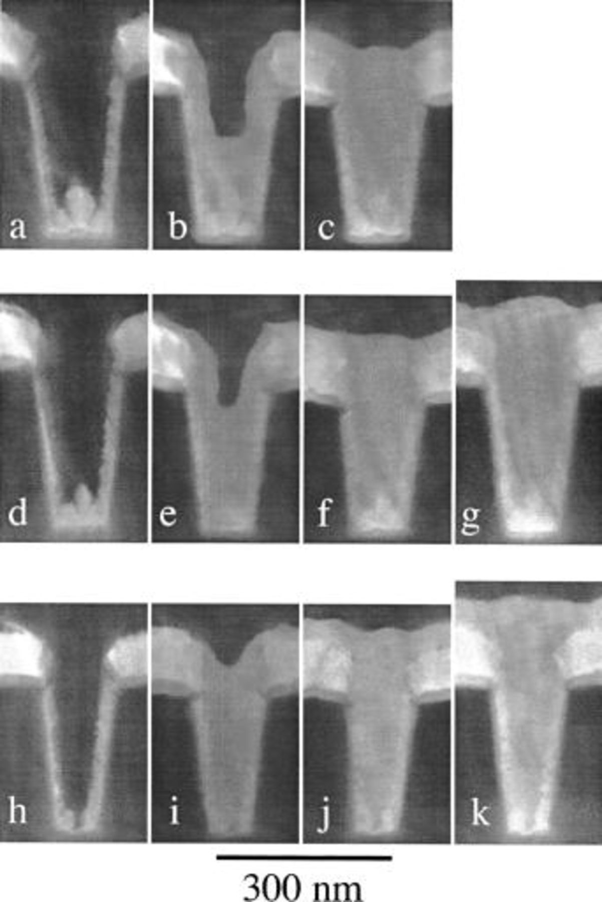
Figure 1. Sequential filling by copper electrodeposition is shown for three different aspect ratio trenches in a-c, d-g, and h-k. Copper electrodeposition times are 3, 6, 9, and 12 s (left to right). The Ti adhesion layer is visible as a thin dark layer beneath the thick, bright Ru layer in the field above the trenches. Trench heights are approximately 200 nm, with some variation visible in the micrographs. Trench widths are approximately 150 nm (top), 120 nm (middle), and 105 nm (bottom) at midheight. A porous, columnar grain structure and protrusions are evident on the sidewalls and bottom of the trenches, respectively. They result from non-normal fluxes of depositing Ru and shadowing by the sidewalls.
Such low density structures are frequently seen in thin films fabricated by glancing angle deposition (GLAD).22 23 In contrast, copper seeds1 2 3 and silver seeds24 fabricated in the same system using similar processing conditions are essentially fully dense. The different behavior is likely a result of much lower surface mobility of the depositing Ru, consistent with its higher melting point (2310°C). These deposits are sufficient for demonstrating seedless, superconformal electrodeposition of copper.
Specimens with smoother ruthenium barriers can be fabricated; observation of superfill in finer features is then possible (Fig. 2). The barriers in these specimens are composed of 10 nm tantalum covered with 20 nm ruthenium (in the field), as compared to 10 nm titanium covered with 70 nm ruthenium for the specimens in Fig. 1. The tilt angle decreased from 15 to 14° during deposition.
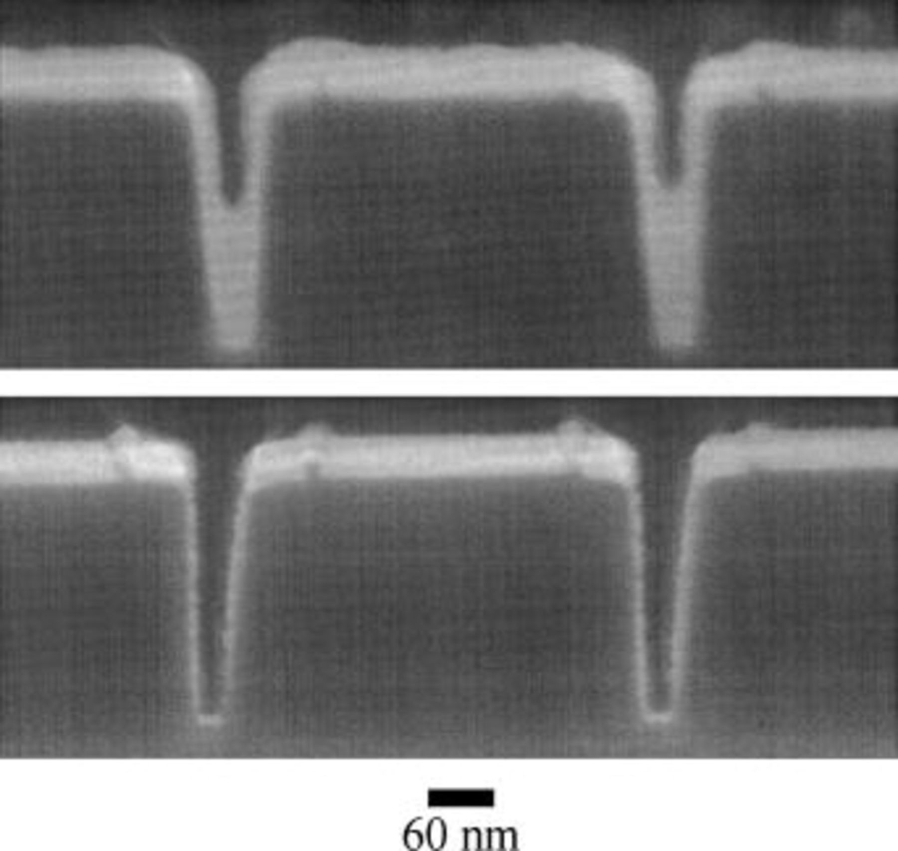
Figure 2. (Top) Two trenches after 7 s of copper electrodeposition. Trench width is approximately 50 nm at midheight. Bottom-up filling is evident. (Bottom) Two trenches showing the tantalum/ruthenium barrier prior to copper deposition.
Copper was electrodeposited onto the ruthenium-coated wafer fragments using an electrolyte containing 1.8 mol/L  0.24 mol/L
  88 μmol/L polyethylene glycol (PEG, Mw 3400 g/mol), 1 mmol/L NaCl, and 50 μmol/L
  (SPS). Electrolytes with similar compositions have been previously shown to yield superconformal deposition of copper in fine trenches and vias possessing copper seeds.1
2
3
4 Samples were plated potentiostatically at −0.2 V vs. a calomel reference electrode (SCE), which corresponds to a copper deposition overpotential of approximately −0.250 V.
(SPS). Electrolytes with similar compositions have been previously shown to yield superconformal deposition of copper in fine trenches and vias possessing copper seeds.1
2
3
4 Samples were plated potentiostatically at −0.2 V vs. a calomel reference electrode (SCE), which corresponds to a copper deposition overpotential of approximately −0.250 V.
After metal deposition, the specimens were covered in epoxy and a glass coverslip and cross sectioned. Polishing was accomplished using diamond lapping films down to 1 μm grit followed by  ion polishing at 13° from the plane of the cross sectioned specimen. Because sputter removal rates of the epoxy and copper were rapid compared to those of the Ru and Si substrate, specimens were shielded so that they only saw the
  flux across the Si substrate. The cross sectioned specimens were examined in a field-emission scanning electron microscope.
Results
Deposition on patterned substrates.—
Deposition results for three different aspect ratio trenches are shown as filling sequences (from left to right) in Fig. 1. Deposition times are 3, 6, 9, and 12 s (from left to right). Bottom-up filling is evident, particularly in the profiles Fig. 1b and e; it is also signaled by the overfill bumps1 2 3 4 in Fig. 1c, f, g, j, and k. Despite the highly irregular surface morphology of the Ru layers, no voids were noted near the Cu/Ru interface (with the exception of voids at breaks in the Ru at the bottoms of the highest aspect ratio trenches (Fig. 1h-k). The quality of fill, despite the initial roughness, is most likely a result of surface smoothing arising from the same mechanism responsible for the superconformal deposition process itself.24
Figure 2 shows some of the finest features studied, approximately 50 nm wide at midheight. The lower image shows two trenches after deposition of the tantalum and ruthenium barrier; the upper image shows the extent of feature filling after 7 s of electrodeposition. The bottom-up fill is an unambiguous demonstration of the ongoing superfill process. Protrusions on both sides of the trenches are merely manifestations of the geometry of the underlying dielectric.
Conclusion
Superconformal copper electrodeposition has been demonstrated in trenches lined with ruthenium. These results demonstrate that copper superfilling does not require the use of a copper seed layer. The Ru layers used in this study are porous and of suboptimal quality which serves to highlight the robust nature of its integration with the copper filling process. The results are conservative in the sense that smoother Ru barriers may be obtained by other processes (i.e., ALD21) and/or processing parameters. In addition to permitting process simplification, further refinement in the combined use of Ru and copper may yield improved performance, i.e., electrical conductivity, relative to conventional metallization.
National Institute of Standards and Technology assisted in meeting the publication costs of this article.