
Abstract
Three different passivation layers  MgO, and
  were examined for their effectiveness in mitigating surface-state-induced current collapse in AlGaN/GaN high electron mobility transistors (HEMTs). The plasma-enhanced chemical vapor deposited
  produced ∼70-75% recovery of the drain-source current, independent of whether
  or
or  plasma chemistries were employed. Both the
  and MgO produced essentially complete recovery of the current in GaN-cap HEMT structures and ∼80-90% recovery in AlGaN-cap structures. The
  had superior long-term stability, with no change in HEMT behavior over 5 months aging. © 2002 The Electrochemical Society. All rights reserved.
Export citation and abstract BibTeX RIS
AlGaN/GaN high electron mobility transistors (HEMTs) show great promise for applications in which high speed and high temperature operations are required, such as high frequency wireless base stations and broad-band links, commercial and military radar, and satellite communications.1
2
3
4
5
6
7
8
9
10
11
12
13
14
15
16
17
18
19
20
21
22
23
24
25
26
27
28
29
30 These devices appear capable of producing very high power densities (>12 W mm−1), along with low noise figures (0.6 dB at 10 GHz) and high breakdown voltage. A number of recent reviews have appeared on this topic.31
32
33
34
35 The use of metal-oxide-semiconductor (MOS) or metal-insulator-semiconductor (MIS) gates for HEMTs produces a number of advantages over the more conventional Schottky metal gates, including lower leakage current and greater voltage swing.3
22
26
28
29
30 Among the materials employed for gate oxide/insulators are  3
25
26
27
28
29
30
42
43
3
25
26
27
28
29
30
42
43  25
26
30
40 AlN,41
25
26
30
40 AlN,41  16
36
37
38
39 MgO,27
44 and
16
36
37
38
39 MgO,27
44 and  44 These materials can also be employed as surface passivation layers on HEMTs. One problem commonly observed in these devices is the so-called current collapse in which the application of a high drain-source voltage leads to a decrease of the drain current and increase in the knee voltage.5
7
14
15
16
17
18
19
20
23 This phenomenon can also be observed by a current dispersion between dc and pulsed test conditions or a degraded rf output power. The cause is the presence of surface states on the cap layer or trapping centers in the resistive buffer underlying the active channel. The carriers in the two-dimensional electron gas can be lost either to the surface or buffer traps.5
7
45
46
47
48 The former may be mitigated to a greater or lesser extent by the use of appropriate surface passivation, most often
44 These materials can also be employed as surface passivation layers on HEMTs. One problem commonly observed in these devices is the so-called current collapse in which the application of a high drain-source voltage leads to a decrease of the drain current and increase in the knee voltage.5
7
14
15
16
17
18
19
20
23 This phenomenon can also be observed by a current dispersion between dc and pulsed test conditions or a degraded rf output power. The cause is the presence of surface states on the cap layer or trapping centers in the resistive buffer underlying the active channel. The carriers in the two-dimensional electron gas can be lost either to the surface or buffer traps.5
7
45
46
47
48 The former may be mitigated to a greater or lesser extent by the use of appropriate surface passivation, most often  deposited by plasma-enhanced chemical vapor deposition (PECVD), while the latter is a function of the epitaxial growth conditions. In the situation in which surface states dominate the current collapse, the use of
  passivation typically restores 70-80% of the lost current.
We have recently found promising results for two alternative candidates for HEMT passivation, namely,  and MgO.49
50 A comparison of the properties of these oxides with those of the other commonly used passivation materials on GaN is shown in Table I. They have smaller lattice mismatch to GaN and larger bandgap than
and MgO.49
50 A comparison of the properties of these oxides with those of the other commonly used passivation materials on GaN is shown in Table I. They have smaller lattice mismatch to GaN and larger bandgap than  In addition, they do not contain hydrogen and may have advantages over
  in that respect because atomic hydrogen diffuses rapidly and could enter the GaN or gate metal over extended periods of device operation.
Table I.
Material properties for GaN and various dielectrics. 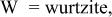    | ||||||||
|---|---|---|---|---|---|---|---|---|
| GaNa |
 b-d
b-d |
 d
d | AlNe-g | GGGh |
 h-j
h-j |
 k
k | MgOl,m | |
| Structure | W | A | A | W or A | A | B | B | N |
| Lattice constant | 3.186 | - | - | 3.113 | 10.813 | 9.845 | 4.2112 | |
| Atomic-spacing inthe (111) plane | - | - | - | - | 3.828 | 3.4807 | 2.978 | |
| Mismatch to GaN(%) | - | - | - | 2.3 | - | 20.1 | 9.2 | −6.5 |
 (K) (K) | 2800 | 1900 | 2173 | 3500 | 2023 | 2668 | 2678 | 3073 |
| Bandgap (eV) | 3.4 | 9 | 5 | 6.2 | 4.7 | 5.3 | 6.3 | 8 |
| Electron affinity(eV) | 3.4 | 0.9 | 0-2.9 | 0.63 | 0.7 | |||
| Work function(eV) | 0.9-1.2 | 2.1-3.3 | 4 | 3.4-4.4 | ||||
| Dielectric constant | 9.5 | 3.9 | 7.5 | 8.5 | 14.2 | 11.4 | 14 | 9.8 |
| a Properties of Group III Nitrides, J. H. Edgar, Editor, Inspector, the Institution of Electrical Engineers, London, U.K. (1994). | ||||||||
| b G. W. Kaye and T. H. Laby, Tables of Physical and Chemical Constants and Some Mathematical Functions, 11th ed, Longmans, New York (1956). | ||||||||
| c C. T. Sah, Fundamentals of Solid-State Electronics, World Scientific, River Edge, NJ (1991). | ||||||||
| d S. M. Sze, Physics of Semiconductor Devices, 2nd ed., Wiley, New York (1981). | ||||||||
| e W. M. Yim, E. J. Stofko, P. J. Zanzucchi, J. I. Pankove, M. Ettenburg, and S. L. Gilbert, J. Appl. Phys., 44, 292 (1973). | ||||||||
| f W. L. Chin, T. L. Tansley, and T. Osotchan, J. Appl. Phys., 75, 7365 (1994). | ||||||||
| g M. S. Shur and M. A. Khan, Mater. Res. Bull., 22(2), 44 (1997). | ||||||||
| h S. S. Derbeneva and S. S. Batsano, Dokl. Chem., 175, 710 (1967). | ||||||||
| i S. S. Batsono and E. V. Dulepov, Soviet Physics—Solid State, 7(4), 995 (1965). | ||||||||
| j K. A. Gschneider, Rare Earth Alloys, Izd. Mir., Moscow (1965). | ||||||||
| k V. N. Abramov, A. N. Ermoshkin, and A. I. Kuznetsov, Sov. Phys. Solid State, 25, 981 (1983). | ||||||||
| l N. Daude, C. Jouanin, and C. Gout, Phys. Rev. B, 15, 2399 (1977). | ||||||||
| m G. V. Samsonov, The Oxide Handbook, Plenum, New York (1973) and references therein. | ||||||||
In this paper we report on a comparison of  MgO, and
  passivation layers on AlGaN/GaN HEMTs with different layer structures (GaN vs. AlGaN cap layer) and show the long-term (5 month) stability of the MgO and
  passivation. We find essentially complete mitigation of the drain current collapse in GaN-capped HEMTs passivated with MgO or
  compared to 70-75% recovery with
  For AlGaN-capped HEMTs, the MgO and
  is effective in restoring ∼80-90% of the drain current.
Experimental
Two different HEMT structures were used in these experiments. The first employed a GaN undoped cap layer on top of an undoped  layer. Both
  and SiC substrates were used. The doping in this structure is basically due to piezo-induced carriers. The second type of HEMT employed an undoped
  cap layer on top of a doped
  donor layer. The doping in this structure is due to the intentional Si doping of the donor layer. The ohmic (Ti/Al/Pt/Au) and gate (Ni/Au) contacts were deposited by E-beam evaporation and patterned by lift-off. Schematics of the completed device structures are shown in Fig. 1.
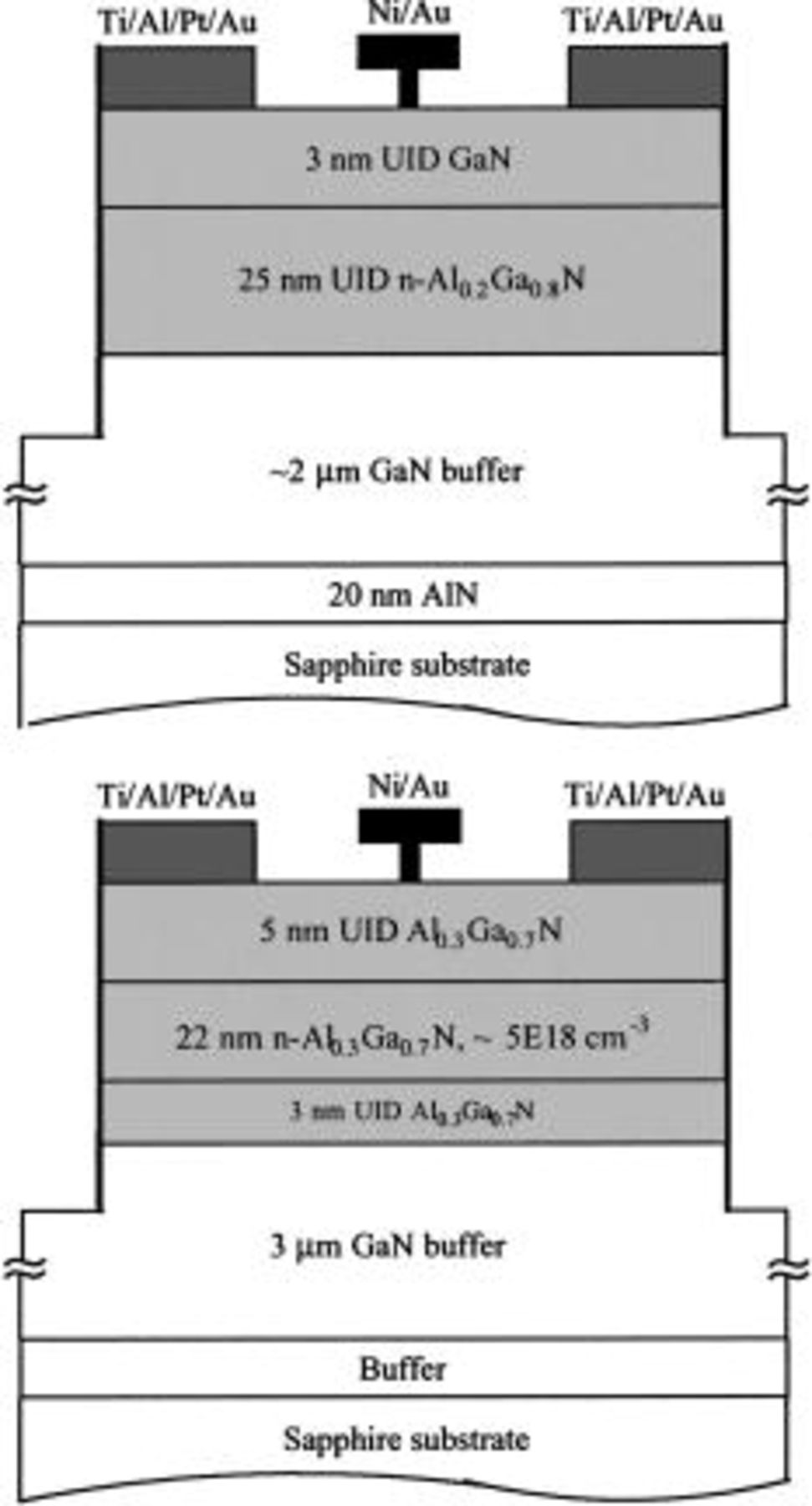
Figure 1. Schematic cross sections of GaN-cap (top) and AlGaN-cap (bottom) HEMT structures.
The 100 μm thick MgO,  or
or  layers were deposited on completed devices (0.25-1.2 μm gate length, 100 μm gate width) using either molecular beam epitaxy (MBE) for the oxides or PECVD for the
  with deposition temperatures of 100°C in the oxide case and 250°C for the
  case. Details of the oxide deposition have been given previously.49
50 The
case. Details of the oxide deposition have been given previously.49
50 The  films were deposited with either
  or
or  to examine the effect of deuterated precursors.
The HEMT dc parameters were measured in dc and pulsed mode at 25°C, using a parameter analyzer for the dc measurements and pulse generator, dc power supply, and oscilloscope for the pulsed measurements. For the gate lag measurements, the gate voltage  was pulsed from −5 to 0 V at different frequencies with a 10% duty cycle.
Results and Discussion
Unpassivated Devices.—
Figure 2 (top) shows typical gate lag data for  GaN-cap HEMT grown on sapphire substrates. The decrease in drain-source current becomes more pronounced at high measurement frequencies. The degradation in current was less significant when these same structures were grown on SiC substrates, as shown in Fig. 2 (bottom). The defect density will be lower in the latter case due to the closer lattice match between GaN and SiC, and this appears to affect the resultant surface state density. This suggests that at least some of the surface traps are related to dislocations threading to the surface.
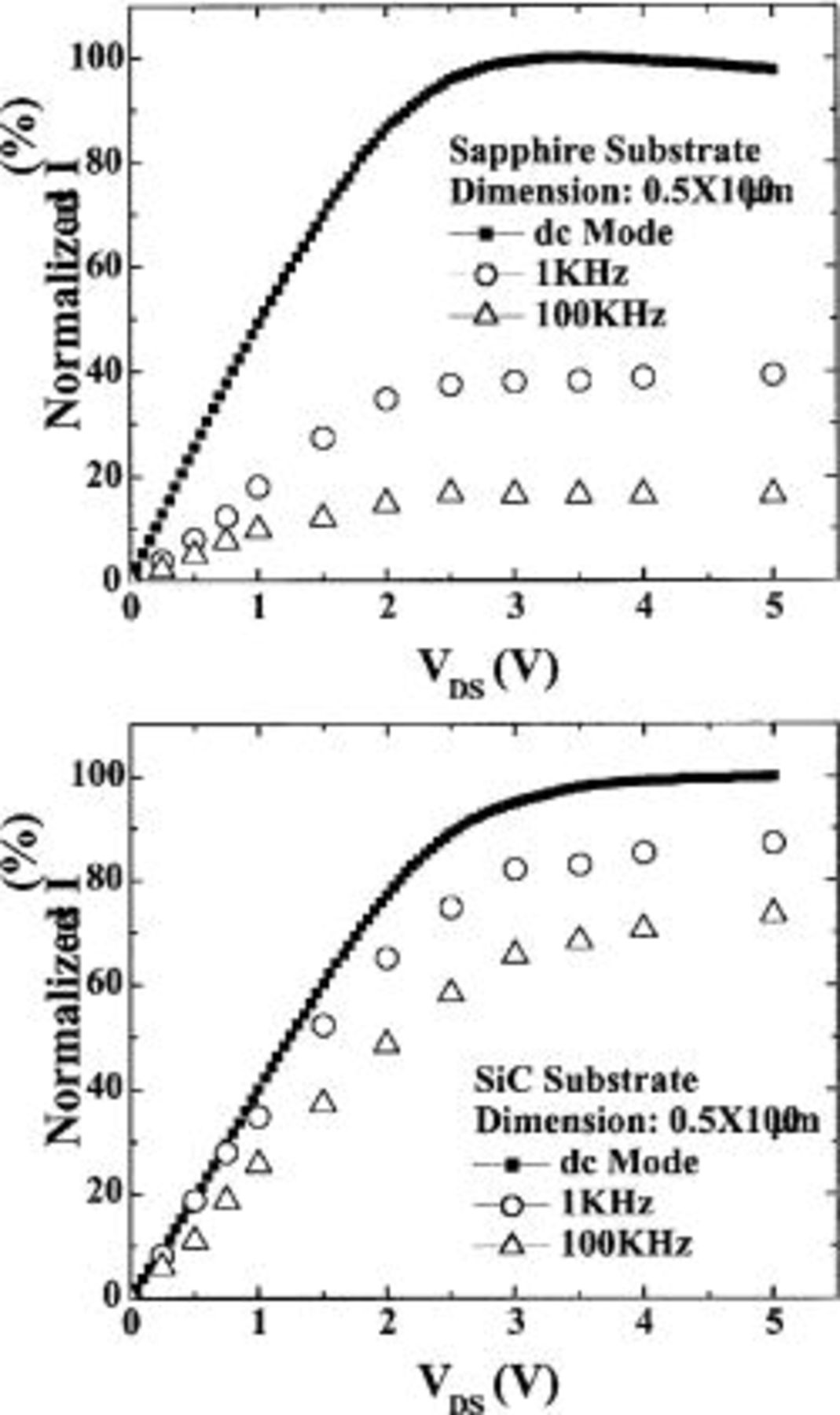
Figure 2. Gate lag measurements on unpassivated 0.5 μm gate length, GaN-cap HEMTs grown on either sapphire (top) or SiC (bottom) substrates.
The effects of both substrate type and HEMT gate length on the change in drain-source current are shown in Fig. 3. The shorter the gate length, the more pronounced the degradation in current because of larger surface area and higher electric field in the channel between source, S, and drain, D (the S-D distance was fixed in all cases).
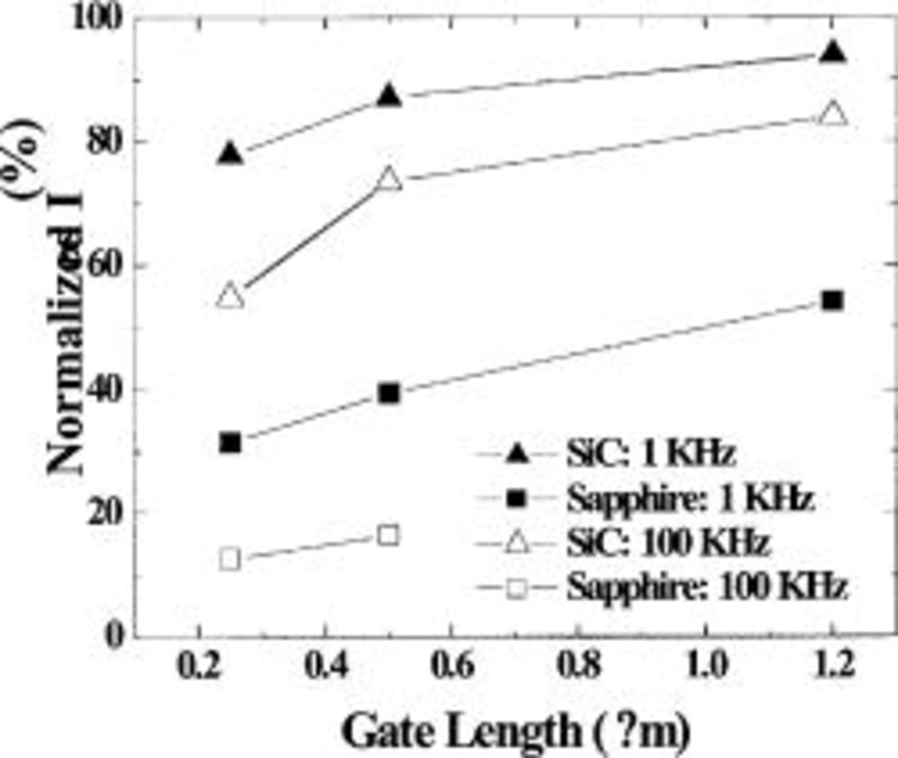
Figure 3. Normalized  as a function of both gate length and substrate type for GaN-cap HEMTs at pulse frequency of 1 and 100 kHz.
 passivation.—

Figure 4 (top) shows the  characteristics before and after
  passivation using either hydrogenated or deuterated precursors. The inset shows the complete set of curves for the as-fabricated HEMT, and the main figure shows only the uppermost curves for clarity. The
  increases after passivation with either type of
  which indicates that the surface state density is decreased.15 Similarly, the transconductance
  increases after
  deposition, which also suggests a decrease in surface trap density (Fig. 4, bottom).15
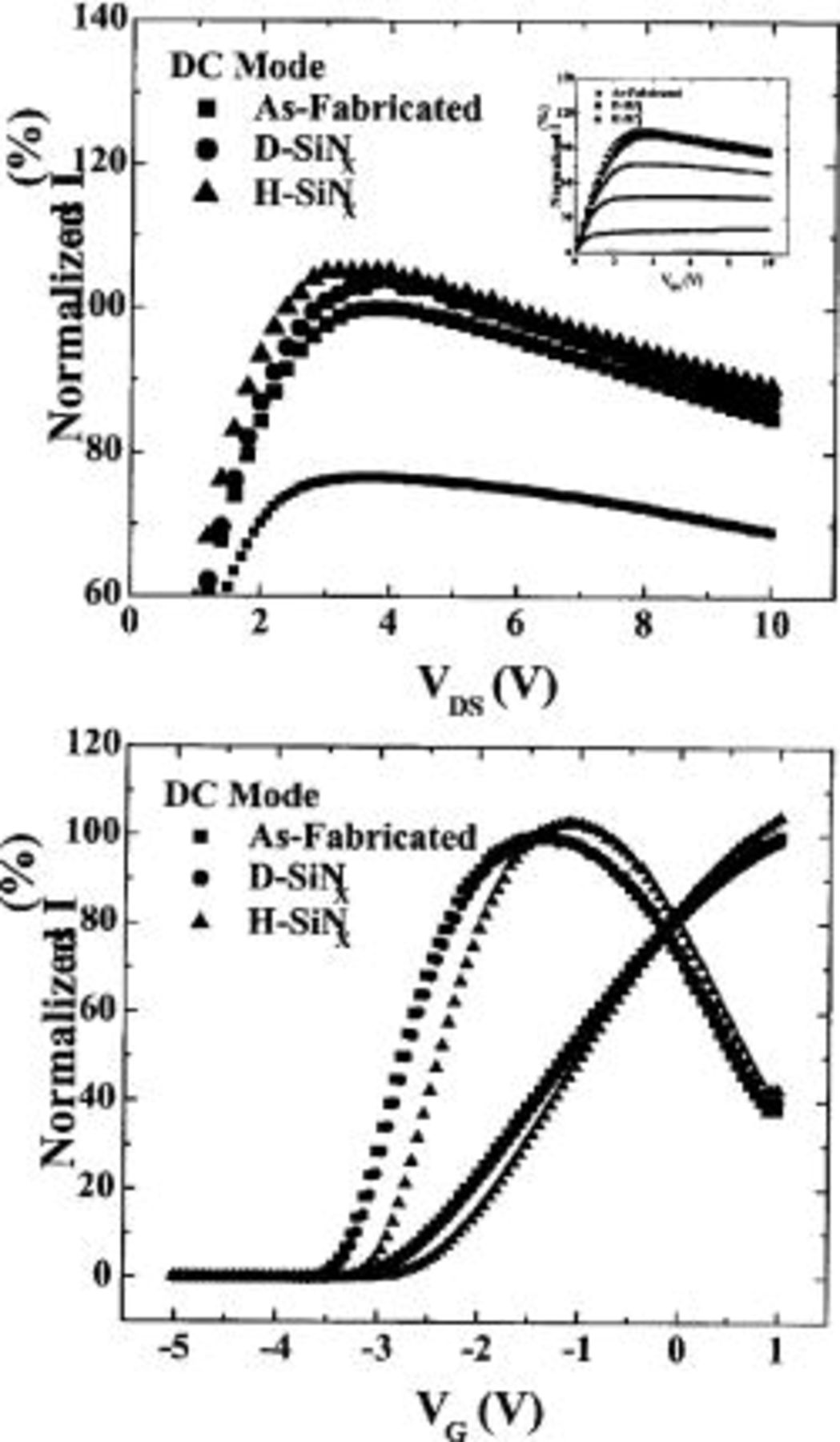
Figure 4. Normalized  vs.
vs.  (top) or
  (bottom) for
  GaN-cap HEMTs before and after
  passivation using either hydrogenated or deuterated precursors.
The gate lag data is shown in Fig. 5 (top) for the HEMTs before and after  passivation. Note that both the hydrogenated and deuterated precursor dielectric produces a recovery of 70-75% in the drain-source current. This range represents results obtained from five different devices with each type of dielectric. The unity current gain frequency
  and maximum frequency of oscillation
  data before and after passivation are shown at the bottom of Fig. 5. Note that there is actually a slight increase in both parameters, in contrast to previous reports.15 There were no systematic differences between the results for hydrogenated and deuterated precursors
  even though the latter typically produce slightly denser films when deposited under the same PECVD conditions.
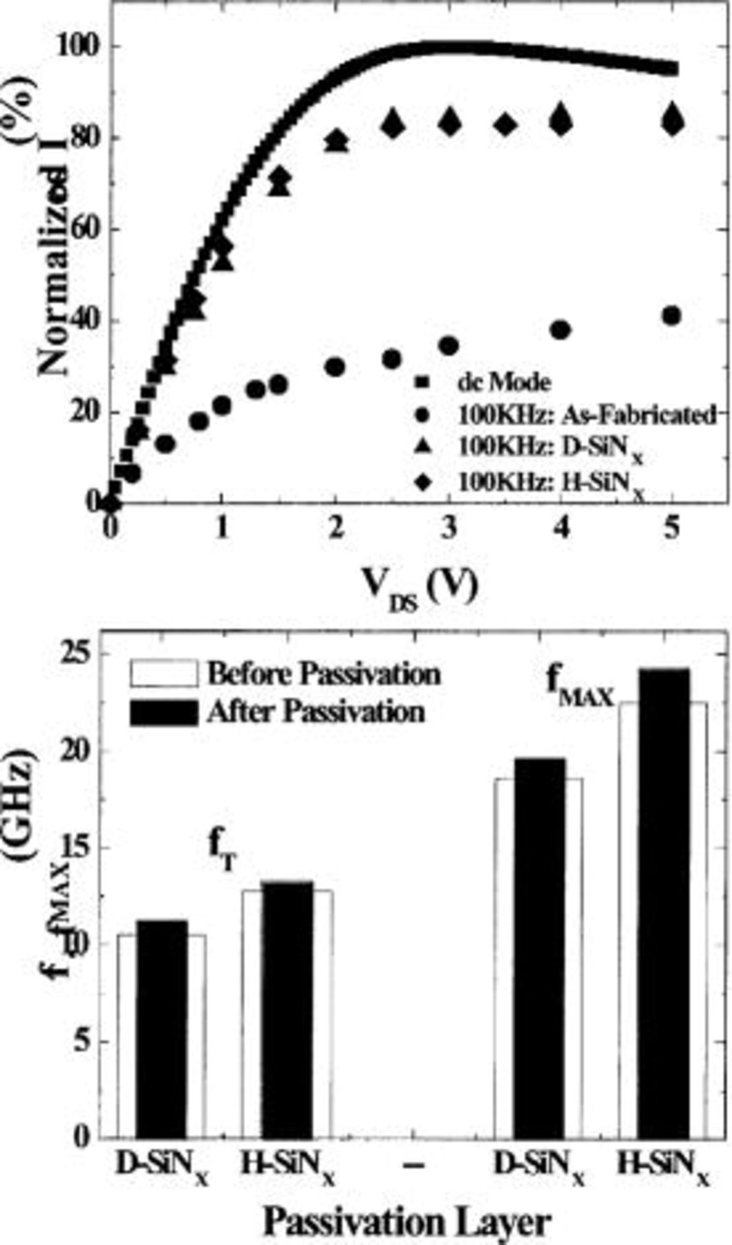
Figure 5. Gate lag measurements before and after  passivation of
 GaN-cap HEMTs (top) and
  and
and  before and after
  passivation (bottom).
There was also an increase in forward and reverse gate currents after passivation with  as shown in the
  characteristics in Fig. 6. These results are also consistent with a decrease in surface depletion and decrease in surface trap density and indicate that there is no major degradation to the dc performance of the HEMTs upon addition of the
  layer. We believe the increase in gate leakage is not from the passivation itself, but may originate from degradation of the gate metallization during the oxide desorption step at 350°C.
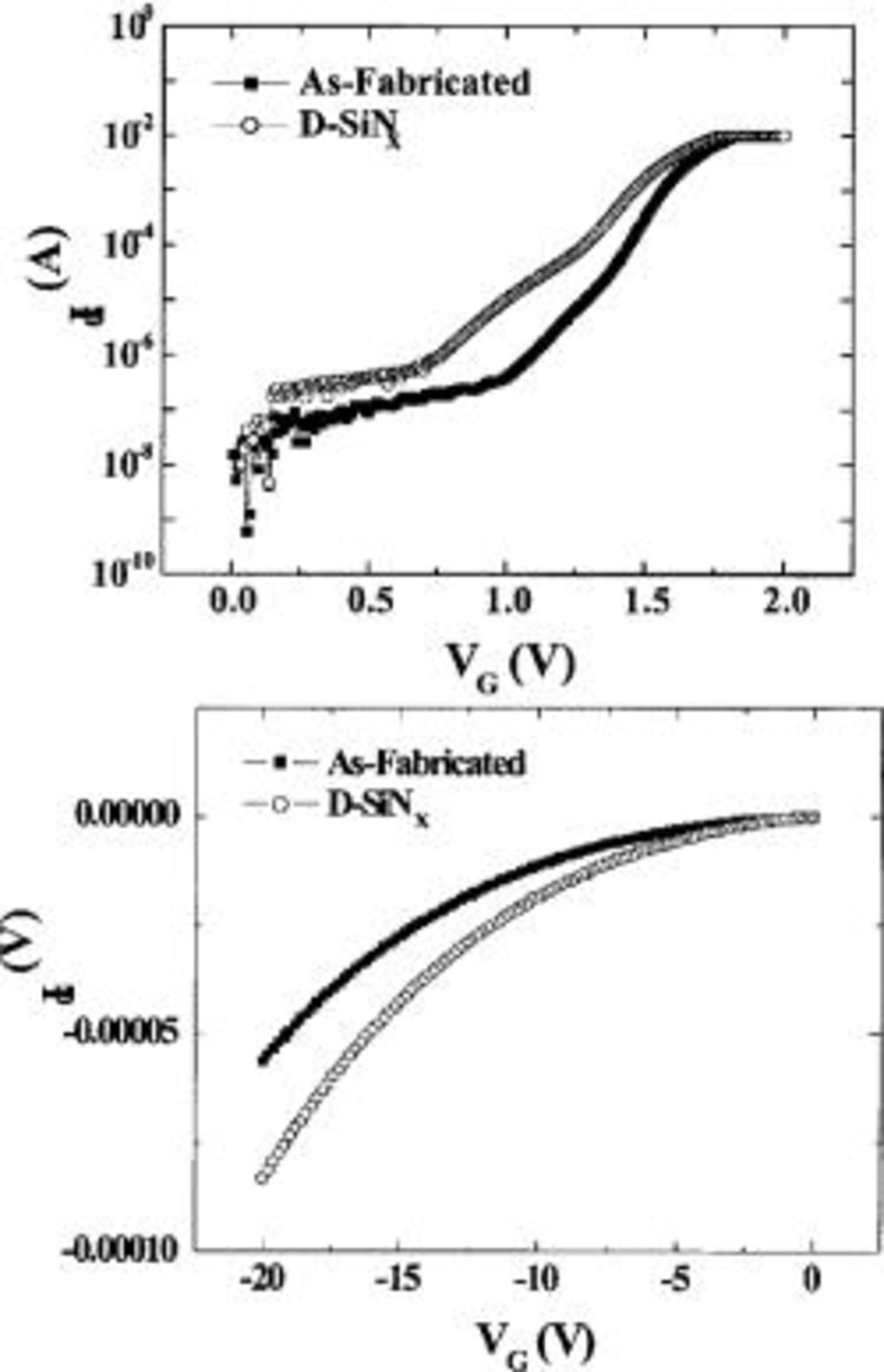
Figure 6. Forward (top) and reverse (bottom)  characteristics from
  GaN-cap HEMTs before and after
  passivation with deuterated precursors.
MgO and passivation of GaN-cap HEMTs.—

Figure 7 shows the gate lag data for GaN-cap  HEMTs. In the case at the top,
  was pulsed from −5 to 0 V at 0.1 MHz with a 10% duty cycle, and this pulsed data is compared to that from dc measurements. The bottom of Fig. 7 shows the normalized
  for gate voltage switched from −5 V with
  held constant at 3 V to avoid any self-heating effects. This data establishes the baseline for measuring the effectiveness of the MgO and
  passivation. As reported previously,45 these HEMTs showed an increase in the drain-source current of ∼20% after deposition of either type of oxide. In addition, the forward and reverse gate currents were slightly increased (Fig. 8 shows an example for an MgO-passivated HEMT). These results are similar to those for
  deposition. Once again, the increased reverse current may be due to gate metal degradation.
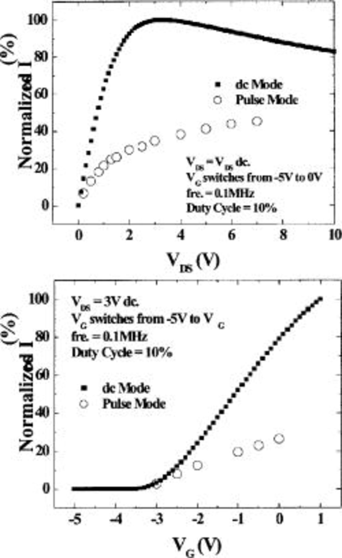
Figure 7. Gate lag measurements on unpassivated GaN-cap HEMTs  gate). At top
  was switched from −5 to 0 V, while at bottom it was switched from −5 V to the value shown on the x axis.
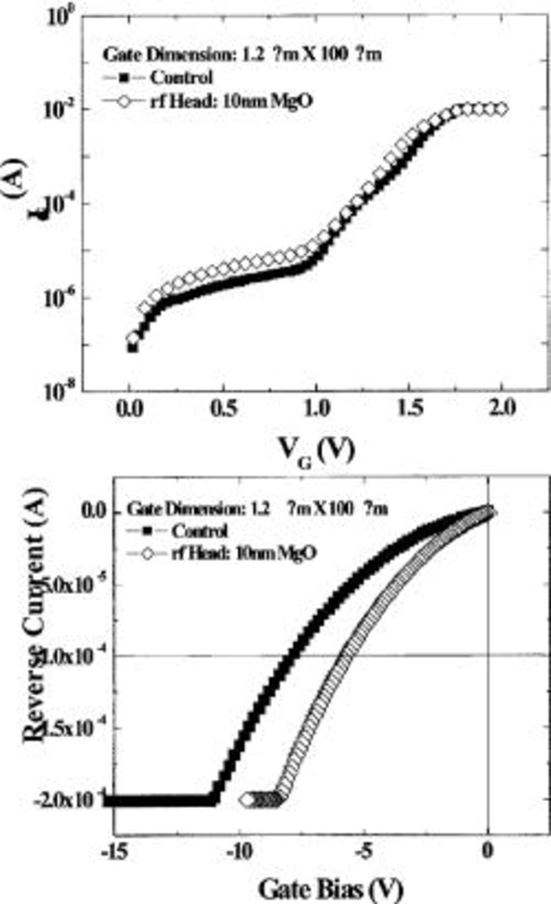
Figure 8. Forward (top) and reverse (bottom)  characteristics from
  GaN-cap HEMTs before and after MgO passivation.
Figure 9 shows gate lag measurement for MgO-passivated HEMTs immediately after MgO deposition and after 5 months aging without bias on the devices under room conditions (temperature and humidity). The  increases ∼20% upon passivation, as mentioned earlier, and there is almost complete mitigation of the degradation in
  immediately after MgO deposition. However after 5 months aging, there is a clear difference between the dc and pulsed data, indicating that the MgO passivation has lost some of its effectiveness. We are currently investigating possible mechanisms such as oxidation of the GaN surface through pinholes in the MgO, or reaction between the MgO and GaN.
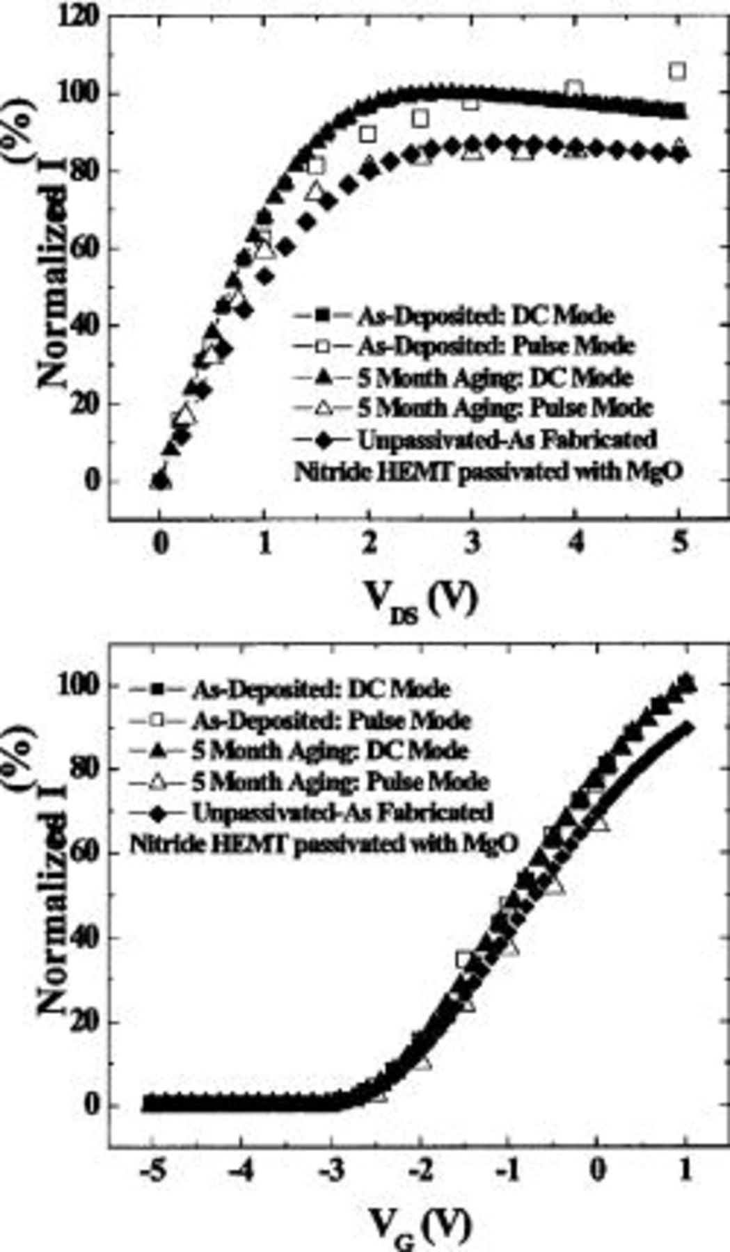
Figure 9. Gate lag measurements before and after MgO passivation and following 5 months aging of  GaN-cap HEMTs. At top
  was switched from −5 to 0 V, while at bottom it was switched from −5 V to the value shown on the x axis.
Similar data is shown in Fig. 10 for  -passivated HEMTs. In this data the
  also increases upon deposition of the oxide, and there is also essentially complete mitigation of the degradation in drain-source current. However the major difference is that these is no significant change in these characteristics after 5 months aging. This indicates that
  provides more stable passivation than MgO. We have noticed in separate experiments that the MgO/GaN interface deteriorates over time if left uncapped, i.e., we see increases in interface state trap density in MOS diodes on which the metal is deposited a long period after the MgO was deposited on the GaN. However, if the MgO is immediately covered by the gate metal, these changes are not observed. In a real manufacturing process, the MgO-passivated HEMTs would be covered with a dielectric such as
  to provide mechanical protection, and thereforeMgO should not be disqualified as a candidate to provide effective passivation of GaN/AlGaN HEMTs. Obviously, further work is needed to establish the reliability of
  and MgO passivation on these devices, but the preliminary data with
  look very promising.
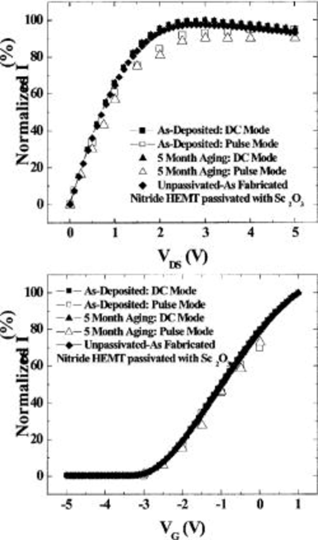
Figure 10. Gate lag measurements before and after  passivation and following 5 months aging of
  GaN-cap HEMTs. At top
  was switched from −5 to 0 V, while at bottom it was switched from −5 V to the value shown on the x axis.
MgO and passivation of AlGaN-cap HEMTs.—

Figure 11 shows the gate lag data for the HEMT structures of Fig. 1 (bottom), i.e., the structures with  as the top layer. As with the GaN-cap devices, there is a very significant degradation of drain-source current under pulsed conditions where the surface traps cannot completely empty.
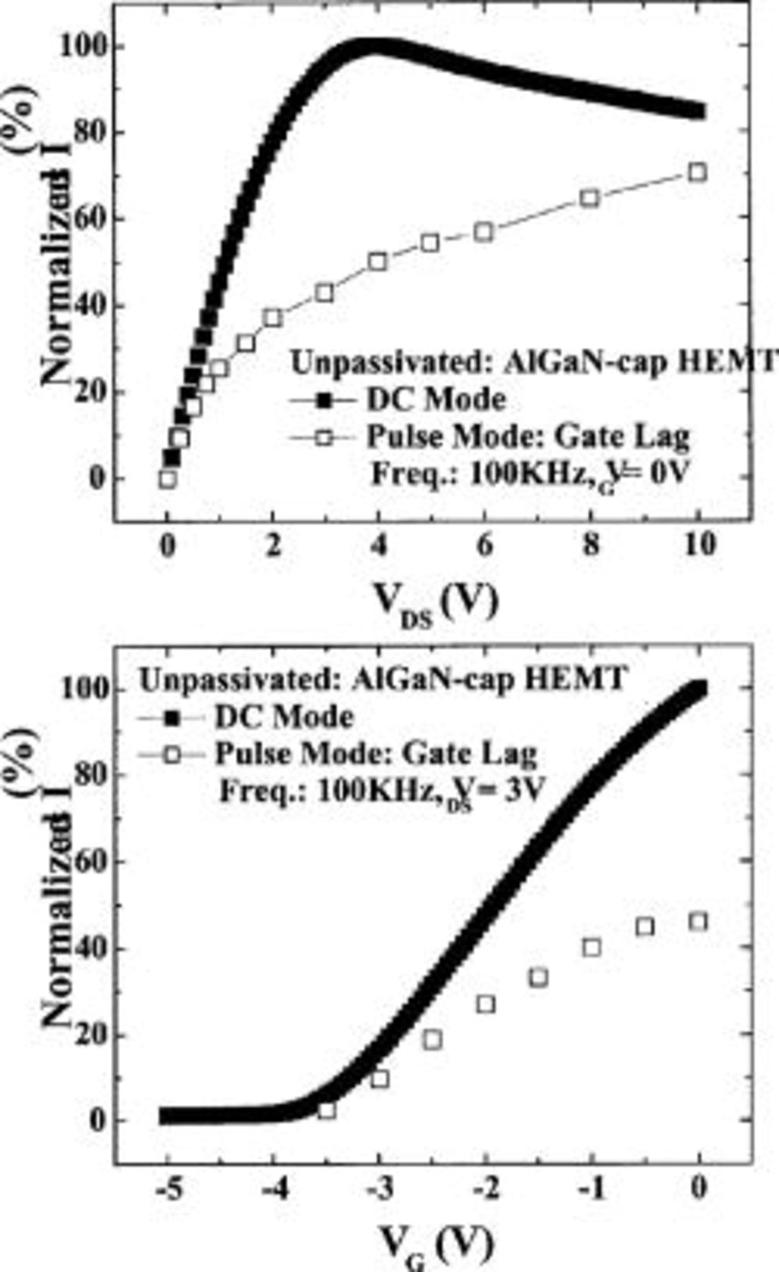
Figure 11. Gate lag measurements on unpassivated 0.5 μm gate length, AlGaN-cap HEMTs. At top  was switched from −5 to 0 V, while at bottom it was switched from −5 V to the value shown on the x axis.
The effectiveness of the MgO and  passivation was more variable on the AlGaN-cap devices than for the GaN-capped HEMTs described in the previous section. Figure 12 shows typical gate-lag data from a
  passivated AlGaN-cap HEMT. We found that the
  deposition was typically able to restore 80-90% of the drain current loss relative to dc measurement conditions. Some devices showed essentially complete restoration of the current, but the 80-90% range was more typical. Similar results were obtained for MgO passivation, as shown in Fig. 13. Once again, some individual HEMTs showed essentially full restoration of
  upon MgO deposition, but a more typical result was that shown in Fig. 13, with 80-90% effectiveness. We believe that our in situ cleaning procedure prior to deposition of these oxides in the MBE chamber is not able to completely remove the native oxide from the AlGaN surface. This limits the effectiveness of the resulting passivation and accounts for the more variable results we observe for the AlGaN-cap devices.
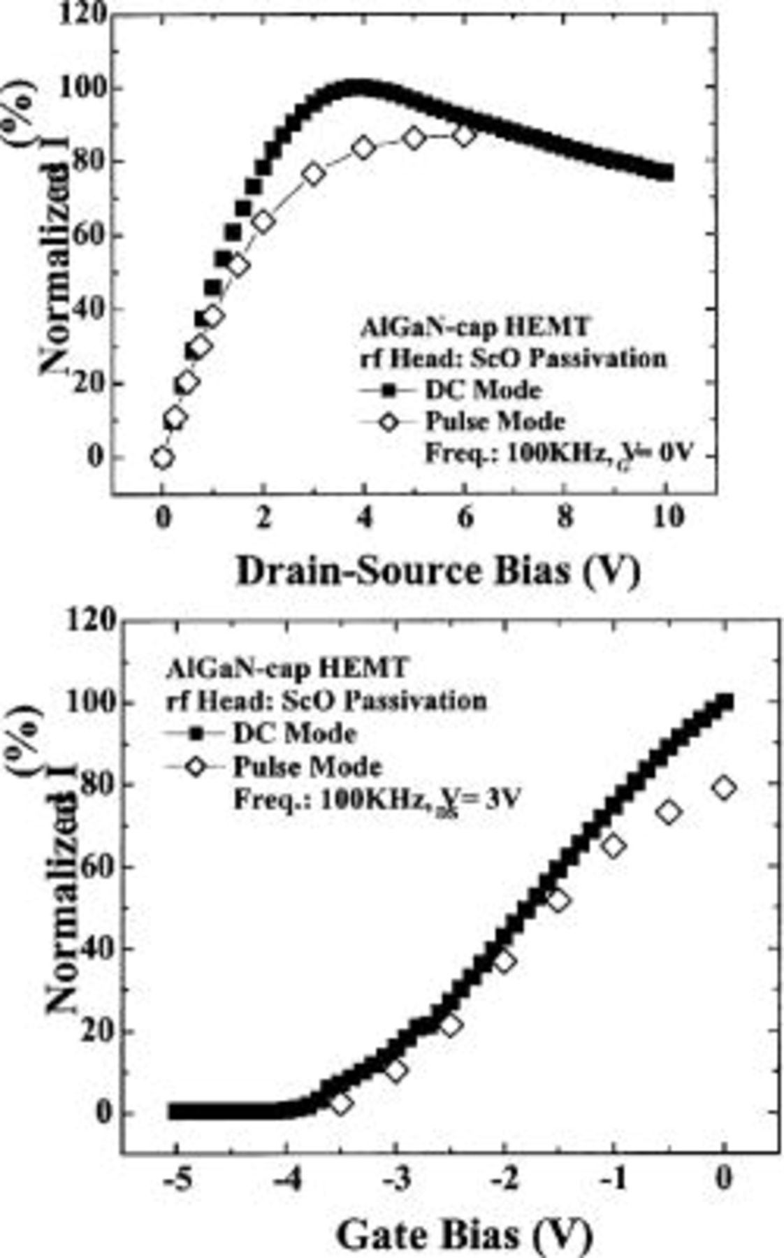
Figure 12. Gate lag measurements before and after  passivation of
  AlGaN-cap HEMTs. At top
  was switched from −5 to 0 V, while at bottom it was switched from −5 V to the value shown on the x axis.
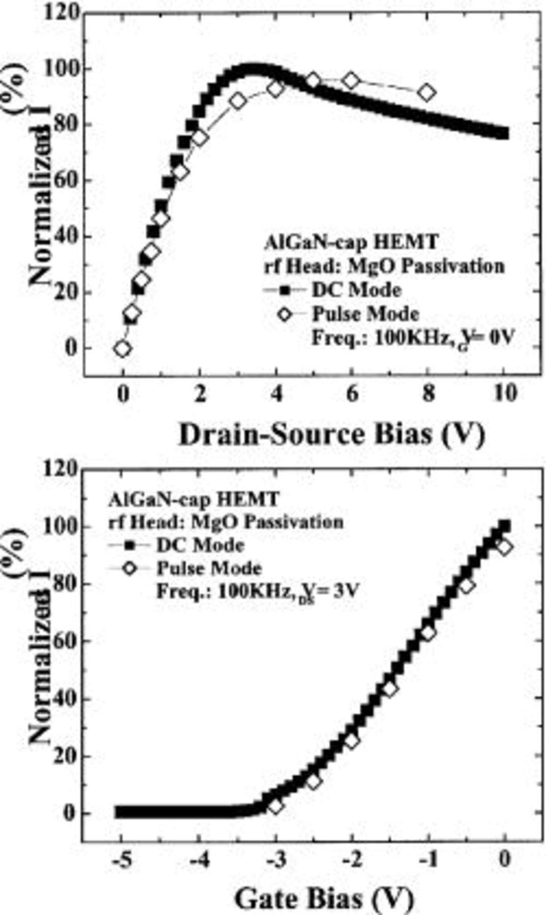
Figure 13. Gate lag measurements before and after  passivation of
  AlGaN-cap HEMTs. At top
  was switched from −5 to 0 V, while at bottom it was switched from −5 V to the value shown on the x axis.
Conclusions
MgO and  thin films deposited by MBE appear very promising as surface passivation layers on AlGaN/GaN HEMTs. In our structures with a GaN-cap layer they provide more effective mitigation of drain current collapse than the conventional PECVD
  films. The
  provides stable passivation characteristics over a period of at least 5 months, while the MgO was found to lose some of its effectiveness under the same conditions. The passivation with both oxides is more variable on AlGaN-cap structures, which we believe is due to the greater difficulties in removing the native oxide from the AlGaN surface prior to deposition of the passivation films. With respect to
  passivation, we found no obvious advantage to the use of deuterated precursors for the deposition. Finally, it should be noted that both MgO and
  can also be used as gate dielectrics on GaN to provide MOS diodes and transistors and thus an MBE system equipped for their deposition can provide both the gate oxide and the device passivation in a manufacturing environment.
Acknowledgments
The work at the University of Florida was partially supported by ONR (H. B. Dietrich, N00014-1-02-04), NSF (DMR010438 and CTS 9901173), and AFOSR F49620-02-1-0366.
University of Florida assisted in meeting the publication costs of this article.