
Abstract
Rare-earth barium-copper-oxide (REBCO) superconductors are high-field superconductors fabricated in a tape geometry that can be utilized in magnet applications well in excess of 20 T. Due to the multilayer architecture of the tape, delamination is one cause of mechanical failure in REBCO tapes. During a mechanical slitting step in the manufacturing process, edge cracks can be introduced into the tape. These cracks are thought to be potential initiation sites for crack propagation in the tapes when subjected to stresses in the fabrication and operation of magnet systems. We sought to understand which layers were the mechanically weakest by locating the crack initiation layer and identifying the geometrical conditions of the slitter that promoted or suppressed crack formation. The described cracking was investigated by selectively etching and characterizing each layer with scanning electron microscopy, laser confocal microscopy, and digital image analysis. Our analysis showed that the average crack lengths in the REBCO, LaMnO3 (LMO) and Al2O3 layers were 34 μm, 28 μm, and 15 μm, respectively. The total number of cracks measured in 30 mm of wire length was between 3000 and 5700 depending on the layer and their crack densities were 102 cracks mm−1 for REBCO, 108 cracks mm−1 for LMO, and 183 cracks mm−1 for Al2O3. These results indicated that there are separate crack initiation mechanisms for the REBCO and the LMO layers, as detailed in the paper. With a better understanding of the crack growth behavior exhibited by REBCO tapes, the fabrication process can be improved to provide a more mechanically stable and cost-effective superconductor.
Export citation and abstract BibTeX RIS
1. Introduction
Coated Conductor (CC) based high temperature superconductor (HTS) technology has advanced significantly in the past few years and CC tapes are now routinely being produced in lengths of several hundreds of meters [1]. High strength Hastelloy alloys have allowed thinner substrates resulting in a significant increase in engineering current density [2, 3], and pinning enhancements in Zr-doped REBCO has increased performance of the wires [4] across a broad range of temperatures and magnetic fields, from 5 T at 77 K [5] up to even 40 T at 4.2 K [6]. These improvements have made REBCO tape a viable option for high energy physics projects [5, 7], fusion reactors such as the SPARC reactor from Commonwealth Fusion Systems [8], and Magnetic Resonance Imaging (MRI) [9, 10]. Although CC tapes provide promise in their electrical performance when compared to their low temperature superconductor (LTS) counterparts, there remain several main challenges associated with REBCO. A key challenge is that, in certain configurations, they are vulnerable to delamination between the different tape layers, due to thermal and magnetic forces experienced during magnet operation [11–13]. REBCO tapes exhibit exceptional axial strength and can withstand up to 700 MPa of stress [14] in that orientation, however when put under a transverse tension, the tape can delaminate under 10–20 MPa of stress [15, 16].
The manufacturing setup and varying application needs of REBCO require REBCO tape fabricated at a fixed width, and then subsequently slit for the final user, typically to between 1 mm and 6 mm width. Slitting enhances the cost-effectiveness of the tape by cutting one production unit into several conductors, and also allows the customer to specify a geometry best suited to the application. Currently most manufacturers use mechanical slitting to accomplish this task, but laser slitting is an emerging technology under investigation [17]. Laser slitting involves directing a high-intensity laser beam onto the surface of the conductor, thereby locally ablating through the material. The laser slitting approach has the benefit of reduced forces on the tape, however it comes with a high financial cost and thermal degradation of tape properties. As a result, mechanical slitting is primarily used at present by REBCO manufacturers. One challenge of mechanical slitting is that it causes micro-cracks to form in the REBCO and underlying buffer layers, which become initiation sites for continued crack formation and propagation [18]. These micro-defects in the wire decrease the mechanical and electromechanical strength of the conductor. For example, the Little Big Coil (LBC) at the National High Magnetic Field Laboratory (NHMFL) has seen a post quench critical current degradation and it is suspected that this degradation is caused by defects introduced during slitting [19], an effect exacerbated by the screening current-induced stress in REBCO tape [20]. Tensile fatigue testing has shown that cracks in the REBCO and buffer layers due to slitting are the main cause of fatigue failure and they will grow as the number of cycles (N) increases [21]. In contrast, compressive fatigue testing showed no crack growth in the REBCO and buffer layers as N increased [22].
The goal of this study was to investigate how the geometry of a mechanical slitter results in damage to the superconducting layer and buffer stack in a REBCO conductor. The damage was investigated using scanning electron microscopy (SEM), laser confocal microscopy and digital image analysis. In locations where the slitting damage revealed the underlying buffer stack, a novel technique was developed using a combination of Auger Electron Spectroscopy (AES), argon sputtering, and statistical analysis to identify the composition and thickness of the exposed layer.
2. Methodology
Figure 1 shows a schematic of the fully processed 2G wire from SuperPower. In this study, the mechanical slitting of the 12 mm wide tape into 2 mm wide tape segments was performed after the metalorganic chemical vapor deposition (MOCVD) step. A schematic of the slitting process is shown in figure 2. Each 2 mm wire was given a number 1–6, and the tape was run through the slitter in two configurations. In one configuration (UP), the samples were slit with the REBCO layer facing up and in the second configuration (DOWN), the samples were slit with the REBCO layer facing down, as detailed in figure 3.

Figure 1. (a) Schematic of REBCO tape architecture [3] and (b) different layers of the buffer stack.
Download figure:
Standard image High-resolution image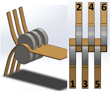
Figure 2. Schematic of the mechanical slitter and the sample naming convention after slitting.
Download figure:
Standard image High-resolution image
Figure 3. Sample orientation schematic relative to the slitter blades, for samples UP (left) and DOWN (right).
Download figure:
Standard image High-resolution imageThe damage near the slit edge in each wire was characterized by scanning electron microscopy (SEM) and scanning laser confocal microscopy (SLCM), and in cases where the REBCO layer had been removed locally by the slitting process, the exposed buffer layer was identified using auger electron spectroscopy (AES). The experiment was divided into two main sections. First, the crack morphology near each damaged edge was observed, the extent of REBCO damage in each sample was quantified, and the identity of the exposed buffer layer was determined. These results appear in section IIIA below. Second, near edges where retained cracks in the REBCO could be observed (i.e. where the REBCO was not fully removed by the slitting process), the length, orientation, and density of cracks was quantified in the REBCO layer and in two of the underlying buffer stack layers, which were exposed by chemical etching. This process and the subsequent results are described in section 3.2 below.
3. Results
3.1. Morphology and composition of the damaged zone near the slit edge
Specimens for investigation were sectioned from samples 1–6 and were imaged on the SEM. Two clear damage patterns emerged from the SEM image analysis. In exactly half of the samples, an approximately 20 μm layer of completely removed REBCO resulted in the exposure of the buffer stack near the slit edge (figure 4(a)). In the other half of the samples, the REBCO was nearly fully retained, however 20–30 μm cracks in the REBCO were visible with a periodicity of ∼5 μm (figure 4(b)). There was a clear pattern dictating which samples showed which behaviour. In the UP orientation samples, the odd-numbered samples (1, 3, 5) exhibited the complete fracturing, and the even-numbered samples (2, 4, 6) exhibited the retained cracks. In the DOWN orientation samples, the behaviour was identical, except that it was the even-numbered samples that exhibited the complete fracturing, and odd-numbered samples exhibited the retained cracks. A likely mechanism for this effect is discussed in section 4 of this paper. Through the remainder of this paper, the vocabulary complete fracturing and retained cracks will be used to identify samples of the type shown in figures 4(a) and (b), respectively.

Figure 4. SEM micrograph of (a) complete fracturing and (b) retained cracks exhibited in the REBCO layer.
Download figure:
Standard image High-resolution imageFor samples exhibiting complete fracturing, confocal laser microscopy was used to acquire additional images of the fractured surface. Samples were imaged at 200× magnification utilizing both white light colour and a 406 nm laser. Contrast between the REBCO and exposed buffer layer was used to perform a greyscale threshold in the image processing software ImageJ. A line segment mask was applied to the threshold to measure the length of the REBCO that had fractured (see figure 5).

Figure 5. The image analysis process for determining width of exposed buffer stack region.
Download figure:
Standard image High-resolution imageThe width of the exposed buffer zone near the slit edge surface was then quantified by digital image analysis. The average exposed buffer zone widths for odd-numbered UP and even-numbered DOWN samples were 23.4 μm and 21.4 μm, respectively. By contrast, the even-numbered UP samples and the odd-numbered DOWN samples (i.e., the retained crack samples) did not show enough exposed buffer layer for clean image analysis to be done (see figure 4(b)), so they were assigned a value of 0 μm. Both sample sets showed similar trends, which suggests that there is no correlation between the damage induced on the samples during slitting and the orientation of the REBCO as it is fed through the slitter. That is, the tape may be fed in either orientation shown in figure 4, with approximately the same results. However, there is a clear periodicity to the locations of the higher and lower levels of damage across the six 2 mm wide samples. This pattern is the same for both UP and DOWN samples, with the only difference being that in the UP configuration, it is the odd-numbered samples that exhibit higher levels of damage, while for the DOWN samples it is the even-numbered samples that exhibit higher levels of damage. This trend is shown quantitatively in figures 6(a) and (b).

Figure 6. (b) Average fracture length for DOWN samples. Odd samples did not show enough fracturing for image analysis, so they were given a value of 0 μm.
Download figure:
Standard image High-resolution imageIn the completely fractured samples, AES was used to identify the exposed buffer layer. In every case examined, the exposed layer was the Y2O3 layer. In addition to determining chemistry, AES can be a useful tool for calculating the thickness of thin films when paired with a sputtering technique using an ion of an inert gas such as argon. The sputter rate of a given material can be calculated by measuring the time it takes to sputter through calibration samples. Most sputter rates are calculated by sputtering SiO2 or Ta2O5. Here, we introduce a technique that calibrates the Y2O3 layer against yttria samples of known thickness to calculate the sputter rate.
To determine the yttria sputter rate, a nine-point grid with approximate dimensions of 30 μm × 30 μm was analysed as a function of sputter time using Ar+ ions in sputter steps of six seconds, as shown in figure 7. AES scans collected yttrium and aluminium signals between sputtering intervals for three different calibration samples processed to just after the deposition of known thicknesses of Y2O3. The yttrium and aluminium signals were normalized to each other and then fit to an error function (equation (1)) as shown in figure 8.


Figure 7. SEM micrograph showing the approximate locations of nine-point scans on a calibration sample.
Download figure:
Standard image High-resolution image
Figure 8. Normalized chemical ratio of yttrium and aluminum as a function of sputtering time, as measured by AES. The cross-over point is used as a convenient reference point to calibrate samples of unknown thickness against samples with known thickness. The nine grid points in figures 6 are averaged together to produce this composite data set.
Download figure:
Standard image High-resolution imageIn this function, t is the sputter time, μ and σ are the mean and standard deviation of the probability density function, respectively, and A and B are fitting terms for the normalization. Once the sputter data was fit to the error function, the time of the crossover point where the aluminium signal surpassed the yttrium signal was calculated. The sputter times and thicknesses of the three calibration samples were graphed and modelled with a linear fit that gave thickness as a function of time, as shown by the open circles of figure 9. This calibration curve was then used to estimate the retained thickness of the yttria in the slit edge samples, as shown by the closed points of figure 9. In figure 9, the thickness of the yttria layer has been plotted on a normalized axis to protect the commercial sensitivity of this information.

Figure 9. AES sputter rate calibration curve after linear fit. The yttria thickness is normalized to the calibration sample with the thickest yttria, in order to protect the commercial sensitivity of the absolute values.
Download figure:
Standard image High-resolution imageThe Ar+ sputtering AES technique was applied to DOWN sample 2 and UP sample 3. From the sputter rate calibration equation, the average thickness of the exposed yttria layer for the two samples was found to be less than the thickness of the calibration samples, which are representative of typical commercial thickness values of the Y2O3 layer. The implication of this finding is that not only is Y2O3 the 'weak link' in the buffer stack that is most susceptible to delamination under the bending forces of the mechanical slitter, but also the delamination is likely occurring within the Y2O3 layer, rather than at the interface of the Y2O3 and MgO layers.
3.2. Retained cracks near the slit edge
As shown in figure 4(b), half of the sample exhibited significant retained cracks near the slit edge. One goal of this study was to understand whether the buffer stacks showed a similar crack distribution as the REBCO layer, and whether the cracks could be spatially correlated to assess the propagation of cracks from one layer to the next. To do this, two adjacent specimens of 4 mm length from sample UP 4 and two adjacent specimens of 4 mm length from sample DOWN 5 were investigated by chemically etching the REBCO layer and selective buffer layers, and analyzing the crack morphology via SEM and confocal microscopy between each etching step. Both the MgO and the Y2O3 buffer layers etched too quickly to isolate, so the REBCO, LaMnO3 (LMO) and Al2O3 layers were analyzed. The REBCO layer was etched using a 2% nitric acid solution for 30 s, revealing the LMO layer. This etch step removes the REBCO and lightly etches the LMO layer for crack definition, in a similar manner as the 2 s etch step of the REBCO layer. The LMO layer and the MgO+Y2O3 layers were etched using the same etchant for 22 min, revealing the Al2O3 layer. AES depth profiling was used to confirm the identity of the LMO and Al2O3 layers by comparing the depth profile to the buffer layer architecture. In this analysis, both slit edges of each sample were characterized for crack density, length, and orientation in each of the three exposed layers shown in figure 10. As shown in figure 11, AES depth profiling was conducted after the 30 s 2% nitric etch step, verifying the presence of LMO via a strong La signal. This La signal gives way over time to the Mg signal as the MgO layer is reached. Similarly, as shown in figure 12, AES depth profiling was conducted after the 21.5 min 2% nitric etch step. With time, the Al signal decreases, and the Ni signal increases, as the Al2O3 layer is eroded and the Hastelloy layer is exposed by the ion beam.

Figure 10. Confocal image stitches showing the nitric acid etching procedure for the REBCO tape.
Download figure:
Standard image High-resolution image
Figure 11. AES depth profile confirming that the LMO layer is exposed after the 30s 2% nitric etch.
Download figure:
Standard image High-resolution image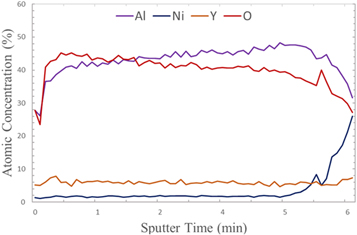
Figure 12. AES depth profile confirming that the Alumina layer is exposed after the 21.5 min 2% nitric etch.
Download figure:
Standard image High-resolution imageAfter SEM images of the edges were stitched together for each layer, lines were manually drawn over every crack in ImageJ and were then digitally processed to collect crack length data, as shown in figure 13.

Figure 13. Demonstration of digital image analysis process on a single SEM micrograph. The manual lines become a data set that can then be processed via quantitative digital image analysis. This process was repeated for the LMO and Al2O3 buffer stack layers.
Download figure:
Standard image High-resolution imageCracks were measured over the full 4 mm length of each sample. SEM micrographs showing representative sections of the REBCO, LMO, and Al2O3 layers that were utilized for this analysis are provided in figure 14. In general, similar crack orientations and morphologies were observed across the three layers, however the cracks differed in length and density among the three layers. In nearly all samples, the REBCO and LMO layers had a similar number of cracks (6.4% higher density in the LMO on average), but the REBCO cracks were on average 21% longer. Moreover, the cracks in the alumina layer were on average 50% shorter and 74% more numerous than the cracks in the other two layers. The crack statistics from each of the two samples analyzed (four locations in each) are summarized in table 1, and the full crack distributions from one location in each samples is shown in figures 15 and 16. Our interpretation of these results is found in section 4 of this paper.

Figure 14. SEM micrographs of sample 4 showing cracks in (a) the REBCO (b) the LMO and (c) the Alumina layers. Red arrows indicate examples of cracks in each layer.
Download figure:
Standard image High-resolution imageTable 1. Crack statistics samples UP 4 and DOWN 5.
| Sample UP 4 | Sample DOWN 5 | |||||
|---|---|---|---|---|---|---|
| Parameter | REBCO | LMO | Al2O3 | REBCO | LMO | Al2O3 |
| Average length (μm) | 48.2 | 39.8 | 17.1 | 21.3 | 18.2 | 13.3 |
| 95% Confidence interval (μm) | 0.90 | 0.84 | 0.33 | 0.40 | 0.27 | 0.17 |
| Total number of cracks | 1508 | 1558 | 3264 | 1686 | 1840 | 2477 |
| Imaged length over four locations (mm) | 16.7 | 16.7 | 16.7 | 14.7 | 14.7 | 14.7 |
| Crack density (cracks mm−1) | 90.5 | 93.5 | 195.9 | 101.2 | 110.4 | 148.7 |
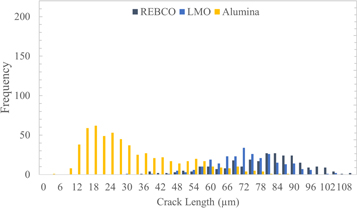
Figure 15. Crack distribution of all three analyzed layers in sample 4 (UP).
Download figure:
Standard image High-resolution image
Figure 16. Crack distribution of all three analyzed layers in sample 5 (DOWN).
Download figure:
Standard image High-resolution image4. Discussion
The mechanical slitting in this work produces two distinct fracture morphologies. The odd-numbered UP samples (1, 3, 5) show complete removal of the REBCO layer to a width of about 20 μm, and the even-numbered DOWN samples (2, 4, 6) show an identical pattern. This clear periodicity correlates with the direction of the bending moment experienced by the REBCO layer of the tape as it passes through the slitter. As shown in figure 17, the forces applied by the mechanical slitter will result in a tensile bending moment on the odd-numbered UP samples, but a compressive bending moment on the even-numbered UP samples. The configuration is exactly the opposite for the DOWN samples. As a result, the cracks that nucleate as a result of the shear strain provided by the slitter can propagate more easily when the REBCO layer is under tensile bending rather than compressive bending. This in turn has a clear and marked effect on the damage pattern observed, and we expect similar damage on the two edges of any individual sample after slitting. This matches the results of other studies in different mechanical configurations such as [21] and [22], where tensile fatigue testing caused REBCO cracks to grow and compressive fatigue testing did not result in crack growth. This crack growth can cause significant degradation in Ic under fatigue conditions which are common in superconducting magnets. For example, in [21] 100,000 cycles to a tensile strain of ε = 0.50% were shown to result in a 70% Ic degradation. Transverse compressive stresses in [22], by contrast, are shown to reduce Ic by less than 1%. Another study compared the lateral distribution of critical current density for different slitting methods and found that when the superconducting layer was under compression during slitting, the equivalent length was less than when the superconducting layer was under tension during slitting [17]. A clear implication is that damage propagation can be minimized by minimizing the extent of tensile bending as the tape passes through the slitter, e.g. by redesigning the device to better support the tape as it passes through.

Figure 17. Visual representation of the bending moments due to slitting relative to the REBCO layer.
Download figure:
Standard image High-resolution image
We further determined the identity of the buffer layer that was exposed when the REBCO layer was fractured and locally delaminated. Across all samples, the exposed layer was yttria and a quantification of the retained thickness indicated that the layer had fractured internally rather than at an interface with an adjacent layer. This indicates that, at least for the tape analysed, the yttria layer acts as a mechanical weak link in the buffer stack.
In the crack length distribution results section, we investigated cracks in narrow damage samples that were a result of slitting. A general trend observed across all samples was that the LMO layer showed more total cracks than the REBCO layer, with the REBCO cracks averaging 21% longer. Another trend that was observed was that the alumina layer showed 74% more cracks than the other two layers, with cracks averaging 50% shorter than those in the other two layers. Spatially, there is excellent matching between the location of cracks in the REBCO layer and those in the LMO layer, indicating that the cracks initiate in one layer and propagate to the adjacent layer. Since the REBCO layer is thicker than LMO by an order of magnitude and located at the maximum bend radius as it goes through the slitter (see figure 17), we can infer that the cracks most likely begin in the REBCO layer and propagate to the LMO layer.
The cracks in the alumina layer, by contrast, are much shorter and more numerous than those in the REBCO or LMO layers. As a result, it is not clear that the alumina cracks propagate to the REBCO/LMO layers or vice versa. Rather, it is more likely that there is a separate crack initiation mechanism governing the damage seen in the Al2O3. For example, the mechanically weak Y2O3 layer may be heavily cracked and initiating the cracking in the Al2O3 (keep in mind that the Y2O3 layer was too thin to isolate via etching and observe in this section of the experiment). Alternatively, the strong and very thick (50 μm) Hastelloy layer adjacent to the Al2O3 may determine its mechanical behaviour. The nature of the crack initiation mechanism in the Al2O3 layer requires further investigation.
5. Conclusions
In this study, we investigated the localized damage caused by the mechanical slitting of REBCO tape after fabrication. For this particular tape configuration, slitting produces a damaged zone of approximately 20 μm in width, and the most aggressive damage occurs when the REBCO layer experienced tensile forces as it passed through the slitter, regardless of the overall orientation of the tape. In cases where the slitting caused local removal of the REBCO layer in this damaged zone, the exposed buffer layer was uniformly Y2O3, and a careful Ar+ AES depth profiling investigation revealed that the Y2O3 fractured internally within the layer, rather than at the interface with the MgO layer. In cases where the slitting did not cause local removal of the REBCO, the crack density and crack length was quantified in the REBCO, LMO, and Al2O3 layers. From the resulting crack distribution, we infer that cracks form both in the REBCO layer and in the Al2O3 layer adjacent to the Hastelloy, and are due to separate initiation mechanisms.
Acknowledgments
This work was financially supported by the U.S. Department of Energy, Office and High Energy Physics, award DE-FG02–13ER42036, and benefited from the support of the Materials Science & Engineering Center at UW-Eau Claire.
Data availability statement
The data that support the findings of this study are available upon reasonable request from the authors.