
Abstract
Efficient thermal radiation in the mid-infrared (M-IR) region is of supreme importance for many applications including thermal imaging and sensing, thermal infrared light sources, infrared spectroscopy, emissivity coatings, and camouflage. The ability to control light makes metasurfaces an attractive platform for infrared applications. Recently, different metamaterials have been proposed to achieve high thermal radiation. To date, broadening the radiation bandwidth of a metasurface emitter (meta-emitter) has become a key goal to enable extensive applications. We experimentally demonstrate a broadband M-IR thermal emitter using stacked nanocavity metasurface consisting of two pairs of circular-shaped dielectric (Si3N4)–metal (Au) stacks. A high thermal radiation can be obtained by engineering the geometry of nanocavity metasurfaces. Such a meta-emitter provides wideband and broad angular absorptance of both p- and s-polarized light, offering a wideband thermal radiation with an average emissivity of more than 80% in the M-IR atmospheric window of 8–14 μm. The experimental illustration together with the theoretical framework establishes a basis for designing broadband thermal emitters, which, as anticipated, will initiate a promising avenue to M-IR sources.
Export citation and abstract BibTeX RIS

Original content from this work may be used under the terms of the Creative Commons Attribution 3.0 license. Any further distribution of this work must maintain attribution to the author(s) and the title of the work, journal citation and DOI.
1. Introduction
For a broad series of applications from chemistry [1] and medicine [2] to atmospheric science [3], the efficiency and bandwidth of light sources will ultimately decide the performance of an entire mid-infrared (M-IR) system. For infrared sensing, it is necessary to capture infrared signals in the atmospheric window (i.e. 8–14 μm) [4, 5], where molecular vibrational fingerprints exist. Taking into account that light sources are the crucial part of numerous M-IR detection systems, so far, a few types of M-IR light sources have been developed. They can be classified into three types: light emitting diodes (LEDs) [6], lasers [7], and thermal emitters [8]. Although the laser can produce a very high output power, the working wavelengths are limited and are not always obtainable for the spectra of interest, not to mention the high cost of infrared lasers. LEDs are much cheaper than lasers, yet their working wavelengths are shorter than 5 μm. M-IR thermal emitters, which depend on heating coiled filaments composed by refractory metals to emit light, are the most popularly employed method to produce M-IR light due to the ultrawide operating spectrum and much cheaper price. Yet, the radiation energy from such an M-IR thermal emitter drops pronouncedly at long-wave M-IR spectrum owing to the low emissivity of the heating filament at this spectrum, making them inappropriate for long-wave M-IR sensing over 8–14 μm. Various nanophotonic thermal emitters have been proposed to operate across a wide spectrum from visible to millimeter [9, 10]. So far, wavelength-scale photonic structures such as silicon carbide (SiC) gratings [11], semiconductor photonic crystals [12], optical antennas [13], resonant cavities [14, 15], and plasmonic nanostructures [16] have been successfully used to engineer the absorptivity that, in turn, tailors thermal radiation following Kirchhoff's law. Of these, an approach using nanofabricated metasurfaces presents promise to modulate infrared thermal emission owing to their significant plasmonic resonance-enhanced Joule loss, directionality, and monochromaticity [17–19]. Such a thermal metasurface emitter (meta-emitter) is very thin because the metasurface can produce near-unity emissivity at the nanoscale, enabling the thermal emission to take place in a much smaller volume than the wavelength of emission in free-space. Since the plasmonic resonance of metasurfaces are associated with their geometries, the metasurfaces are limited to a narrow spectral region. However, a resonance near-unity emissivity over a broad spectral regime is highly desired for wide applications from thermal sensing [20] to infrared imaging [21].
A highly efficient thermal emitter is required to eliminate reflection and transmission across a wide spectrum. Therefore, one needs to consider three key components when designing a meta-emitter: robust light coupling for high absorption [3], large density of optical modes [22], and efficient antireflection [23]. Many works in this area concentrate on tapered or multi-resonance metasurfaces to broaden bandwidth [24, 25]. For example, a hyperbolic metasurface waveguide taper array was demonstrated to increase thermal emission in the short-wave M-IR region between 3 and 5 μm [26]. Nevertheless, practical device applications are limited by the complicated nanofabrication requirements of trapezoidal arrays. Another strategy is to unite various kinds of plasmonic resonators within a subwavelength meta-atom, which can achieve broadband or multiband response [16, 27]. However, the combination of resonators within a subwavelength pitch increases the complexity of the fabrication process and decreases the duty ratio and efficiency of emitter cells [28]. Such limitations may hinder the widespread applications of these meta-emitters. Thus, it is important to develop an efficient wideband thermal emitter that has a straightforward structure, is easy to fabricate, and works in the M-IR atmospheric transparency window.
Herein, we experimentally develop a high efficiency and wideband thermal meta-emitter for long-wave M-IR light production, which has emissivity of ∼80% ranging from λ = 8 to 14 μm. The meta-emitter consists of two pairs of circular–patterned dielectric silicon nitride (Si3N4)–gold (Au) stacks on top of a Si3N4/Au dual-layered structure. We attribute the broadband high emissivity to the combination of propagation surface plasmon resonance (PSPR) and multiple gap plasmon resonance (GPR). The PSPR is strongly related to the period of metasurface. The GPR is supported by the metal-dielectric-metal (MDM) cavity structures with different dielectric thicknesses. In our proposed stacked nanocavity meta-emitter, the Au cylinders and the Au bottom reflector act as mirrors, while the Si3N4 cylinders and Si3N4 dielectric layer represent the dielectric spacers. Note that the near-unit emissivity can be upheld over a broad range of observation angles (θ) from 0° to 60° and is independent of the polarization of light. In contrast to the current commercial M-IR thermal emitter based upon refractory metals, our proposed stacked nanocavity meta-emitter can pronouncedly boost thermal emissivity over the entire long-wavelength atmospheric transparency window of 8–14 μm. The rather simple meta-emitter can be fabricated via a magnetron sputtering system and standard optical lithography techniques, opening possibilities to obtain cost-effective, compact, and wafer-scale fabrication of an M-IR light source.
2. Results and discussions
The broadband M-IR meta-emitter residing on a silicon (Si) substrate was composed by arrays of circular-patterned Au–Si3N4 stacked nanocavities on a Au–Si3N4 dual-layered film, shown in figure 1(a). The inset presents a single period of meta-atoms with designed geometrical parameters. The parameters were optimized to achieve a high emissivity in the spectral range of 8–14 μm. The resonator relies upon three stacked MDM cavities with different cavity lengths that can excite not only the PSPR mode but also three GPR modes in the M-IR region. A hybrid interference between the PSPR and multiple GPR modes leads to a high emissivity spanning the spectrum ranging from 8 to 14 μm. In figure 1(b), we present a top scanning electron microscope (SEM) image of the meta-emitter. We pattern the cylinder array using optical lithography (see 'fabrication section' for details). The schematic of the fabrication process is shown in supplementary figure S1 (available online at stacks.iop.org/IJEM/4/015402/mmedia). The thicknesses of each layer of two pairs of circular-shaped Si3N4–Au stacks, a Si3N4 spacer, and an Au reflector are t1 = 100 nm, t2 = 500 nm, t3 = 300 nm, t4 = 700 nm and t5 = 200 nm, respectively (inset of figure 1(a)).
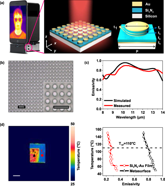
Figure 1. Configuration of the meta-emitter. (a) Schematic of the meta-emitter. The thicknesses of each layer of two pairs of circular-shaped Si3N4–Au stacks, the Si3N4 spacer, and the Au reflector are t1 = 100 nm, t2 = 500 nm, t3 = 300 nm, t4 = 700 nm and t5 = 200 nm, respectively. The pitch in both x- and y-axes is P = 6 μm and radius of the circular disk is r = 4 μm. The entire meta-emitter was deposited onto a Si substrate with 450 μm thickness. Inset: representation of the meta-atom. (b) The SEM image for the top view of the meta-emitter. The meta-emitter has an area of 1500 000 antennae. Scale bar: 10 μm. (c) The Fourier-transform infrared (FTIR) measured (red line) and finite-difference time-domain (FDTD) simulated (black line) ε(ω) spectra of the meta-emitter. (d) The ε(ω) measurements were taken using a thermal camera. Left-column: thermal image of the structure where TD and Tb represent temperatures of the meta-emitter and the unpatterned Si3N4–Au dual-layered structure, respectively. Scale bar: 5 mm. Right-column: the calculated TD and Tb against ε(ω). The ε(ω) is measured under room temperature at 25 °C.
Download figure:
Standard image High-resolution imageSi3N4 is a crucial material employed in bolometer applications due to its advantageous mechanical and thermal features [29]. For this study, Si3N4 was selected as a dielectric film because its dielectric property possesses a large imaginary part over a broadband M-IR regime, indicating a high absorption coefficient. In supplementary figure S2, we experimentally presented the complex refractive index (NSiN = nSiN + i × kSiN) of a 100 nm thick Si3N4 layer on a Si substrate. Variable angle spectroscopic ellipsometry variable angle spectroscopic ellipsometer (VASE) was used to measure the NSiN. A Gaussian model was employed for the fitting. The imaginary part (kSiN, red line) is above 1 across the M-IR region ranging from 9.6 to 13 μm.
Thermal radiation is the emission of a light wave by an item at a temperature greater than absolute zero. The spectrum and intensity of thermal emission depend on the frequency (ω). According to the Kirchhoff's law of thermal radiation, the emissivity (ε(ω)) of a blackbody is the same as its absorptivity (A(ω)) in thermodynamic equilibrium [12, 30]; hence, the A(ω) can be engineered to obtain the desired ε(ω). The structure is designed to possess an extremely low reflectance (R(ω)) in the spectral range from 8 to 14 μm, producing a near-unity A(ω). Thus, our proposed structure acts like a blackbody with the emissivity ε(ω) = A(ω). Kirchhoff's law can be fully validated since the area of our fabricated nanocavity metasurfaces (0.9 cm × 0.7 cm) is much larger than the M-IR wavelength. Since the metasurface is not transparent in the M-IRregion (i.e. the transmitted power is zero), the reflectance is directly measured via a FTIR spectrometer integrated with an infrared microscope (see 'experimental section') [31]. We can then derive the thermal emissivity via ε(ω) = 1 − R(ω). The reflectance measurement was performed under normal incidence. The FTIR measured ε(ω) (red line) are shown in figure 1(c) together with the numerically calculated one (black line). We experimentally obtain a high emissivity of over 0.8 across the spectral range of 9–13 μm that corresponds to thermal radiation. It is clear that a broadband near-perfect emissivity is achieved with the coupling of four independent emissivity peaks, with peak values of 0.71, 0.81, 0.96, and 0.84 at the wavelengths of 8.0, 9.2, 10.4 and 13.2 μm accordingly. These four resonance peaks are expected to account for this broadband high emissivity [32, 33]. Compared to commonly used refractory metal thermal materials (e.g. Ni, Cr, and W) that produce high emissivity in the visible and near-infrared regions and low emissivity at the M-IR region, our proposed meta-emitter can provide a near-unity emissivity over a broad M-IR range. As was seen, the ε(ω) of our device over 8–14 μm is as large as ∼0.8, which is ∼10 to ∼50 times larger than that of Cr and W thermal emitters, respectively. Such a feature makes our proposed structure a very efficient M-IR thermal light source for detecting. The physical mechanism of our meta-emitter depends on not only the PSPR mode of the stacked nanocavity array but the multiple GPR modes supported by stacked MDM nanocavities. The pitch of the stacked nanocavity array and the geometry of the stacked nanocavity resonator (i.e. the radius of the cylinder and the thickness of each layer) that significantly affect the resonances were optimized to allow for both impedance matching and high emissivity, and the cylinder resonator offers polarization independent excitation of resonances [34]. The simulated spectrum of ε(ω) has an excellent agreement with the measured one. As was seen in figure 1(c), we calculated the ε(ω) spectrum using the FDTD method solver. The geometrical parameters of the metasurface were set to those measured using the SEM pictures shown in figure 1(b). The refractive indices of all materials are obtained from experimentally measured data [35]. The details of the numerical model are shown in the 'simulation section'. We further use a thermal camera to study the ε(ω) of the meta-emitter. We can achieve ε(ω) of the meta-emitter by heating up the structure with a reference material having known ε(ω). A method was then developed to solve the ε(ω) of an unknown sample, that is, at thermal equilibrium, the temperature recorded by the thermal camera should be identical to both materials. To precisely measure the meta-emitter temperature, we subtracted the external contributions (e.g. the thermal emission produced by imaging optics and the ambient thermal emission reflected from meta-emitter) from the total thermal emission imposed on camera sensor. (see supplementary figure S3(a)). In the left column of figure 1(d), we present the thermal picture of the meta-emitter heated to 150 °C (the measured thermal image of the meta-emitter under room temperature, Tr = 20 °C, is shown in supplementary figure S3(b)) where the red region presents the meta-emitter. A reference temperature (Tref) of 110 °C is given by the thermal image of the reference black electrical tape (see supplementary figure S3(c)). In the right column of figure 1(d), we calculated ε(ω) dependent temperature for both meta-emitter (TD) and the Si3N4–Au dual-layered structure surrounding it (Tb). The meta-emitter's ε(ω) is larger than ε(ω) > 0.8 and ε(ω) in the unpatterned dual-layered structure is only ε(ω) ∼ 0.3. These values match the qualitative ε(ω) values obtained from FTIR measurement.
An ideal thermal emitter needs to maintain polarization independent high ε(ω) over a broad observation angle (θ) [36]. In figure 2, we experimentally (figure 2(a)) and numerically (figure 2(b)) present ε(ω) as a function of wavelength and θ in the stacked nanocavity metasurfaces on Si substrate, with the left and right columns showing the ε(ω) for p- and s-polarized incident lights, respectively. The observation angle dependent ε(ω) was characterized using an M-IR J. A. Woollam variable angle spectroscopic ellipsometer (VASE). The θ varied from 31° to 81° at a step of 1°. The meta-emitter possesses omnidirectional large ε(ω) for both p- and s-polarization states. As shown in figure 2(a), for the p-polarization state, the ε(ω) is larger than 0.85 for all θ and wavelengths (left column). For the s–polarization state, the ε(ω) decreases at the wider θ; yet, the ε(ω) larger than 0.8 is upheld for θ < 60° (right column). This is due to fact that the direction of the H-field of p-polarized light does not vary pronouncedly with θ and it can produce looped currents at all incident angles. On the other hand, for the s-polarization, the H-field less effectively drives the circulating currents at wide angles [37]. However, a good spectral overlap occurs between the ε(ω) for p- and s- polarization states. We conclude that the meta-emitter is not only polarization-insensitive but omnidirectional. As was seen in figure 2(b), the numerical simulation matches the performance of the fabricated device, and we attribute the difference in the locations of some resonances to radiation scattering from fabrication errors [38]. On the other hand, several factors that may cause the difference are not considered in the numerical model. These factors include the fabrication imperfections, such as the thickness of the native oxide layer and grain boundaries.
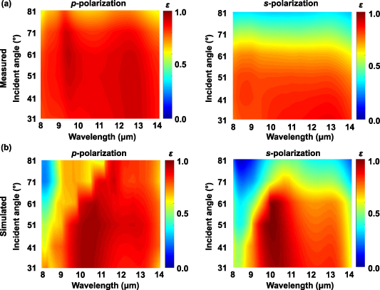
Figure 2. The (a) measured and (b) simulated angular dispersion of the emissivity for the stacked nanocavity meta-emitter for the p-polarization (left column) and s-polarization (right column) states, respectively. The ε(ω) is measured under room temperature at 25 °C.
Download figure:
Standard image High-resolution imageIn figure 3(a), we numerically present ε(ω) of the meta-emitter and Si3N4/Au dual-layered structure under normal illumination. The multilayered metasurface has a high emissivity over a broad M-IR region (8–14 μm) due to the hybrid mode interference of PSPR and GSPR [39]. Whilst the Si3N4/Au dual-layered structure exhibited a much smaller emissivity due to the absence of the plasmon resonance, its emissivity peak around λ = 13.2 μm is caused by an asymmetric Fabry–Pérot cavity composed of a 700 nm thick Si3N4 dielectric film sandwiched between a 200 nm thick Au reflector and air [40, 41]. It suggests that the design of the stacked nanocavity array on the Si3N4/Au film is an extremely efficient device for radiating thermal energy in the M-IR region. To explore the underlying mechanism of the broadband high emissivity, it is instructive to study the magnetic (H)-field distribution for the various resonance modes in the stacked nanocavity metasurface, along the cross-section plane, x–z presented in figure 1. Figures 3(b)–(e) presents the distributions of total magnetic fields ( ) and the displacement current (JD) at the PSPR mode (λ1 = 10.4 μm) [42] and three GPR modes (λ2 = 8.0 μm, λ3 = 9.2 μm, and λ4 = 13.2 μm), respectively, where the color and arrows represent the magnitude of the H-field intensities and JD, respectively. In the meta-emitter, the PSPR mode is associated with delocalized plasmon (or photonic mode coupling) and surface plasmon (SP) that strongly depends on the pitch of meta-emitter [43]. The PSPR can be produced when the pitch is on the order of the working wavelength [44]. As was seen in figure 3(b), the H-field at λ1 = 10.4 μm can be strongly confined between two neighboring resonators, confirming that the emissivity stems from the metasurface induced PSPR. On the other hand, the three GPR induced emissivity peaks at λ2 = 8.0 μm, λ3 = 9.2 μm, and λ4 = 13.2 μm are supported by the cavity between the Au reflectors as presented in similar MDM structures [45]. Herein, the GPR modes are strongly dependent upon the radius of the circular stacked nanocavity and the thickness of each layer. For the GPR modes, the dipolar oscillation of the free electrons in the upper Au cylinders causes an anti-parallel dipolar oscillation in the bottom film, which forms JD loops to effectively produce magnetic dipolar moments for the MDM nanocavity structures [46]. Such magnetic moments can strongly interact with the incident light beam, and finally, the magnetic resonance can be produced in the dielectric space layers [47]. As observed in figures 3(c)–(e), the H-fields at the three GPR wavelength of λ2 = 8.0 μm, λ3 = 9.2 μm, and λ4 = 13.2 μm are concentrated in three Si3N4 dielectric layers with different thicknesses of t2 = 500 nm, t3 = 300 nm, and t4 = 700 nm. The GPR at λ2 = 8.0 nm occurs in the first Si3N4 dielectric layer (figure 3(c)), where the H-field can be efficiently confined in the top Si3N4 layer, whilst the confinements of H-fields are relatively weak in the middle and bottom Si3N4 layers. The GPR at λ3 = 9.2 nm mainly occurs in the middle Si3N4 layer (figure 3(d)), while the H-field is intensely confined in the bottom Si3N4 layer at λ4 = 13.2 μm (figure 3(e)). This is owing to the hybridized mode of the magnetic resonance exciting in the individual Si3N4 layers [48]. In our stacked nanocavity metasurface, both the top and sandwiched Au layers are very thin, which enables the light to propagate through them. Thus, the magnetic resonance moments in the three Si3N4 layers can interfere strongly with each other. Namely, the three GPR modes exciting in the stacked nanocavity metasurface are related to the hybrid magnetic resonances coupled in the three Si3N4 layers. Thereby, the broadband high emissivity in the meta-emitter owes to the hybrid interference of PSPR and multiple GPR modes.
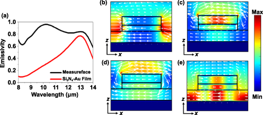
Figure 3. The FDTD simulation of (a) emissivity of both stacked nanocavity metasurface (black line) and Si3N4–Au dual-layered structure (red line), (b)–(e) total H-field intensity distributions along the x–z plane for the meta-emitter at (b) λ1 = 10.4 μm, (c) λ2 = 8.0 μm, (d) λ3 = 9.2 μm, and (e) λ4 = 13.2 μm. The white arrows represent the displacement current. The black line circles the geometrical profile of the structure.
Download figure:
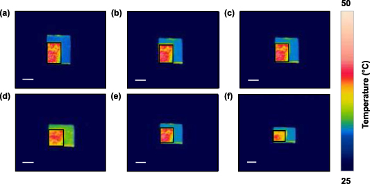
Standard image High-resolution imageThe robustness of the thermal meta-emitter to the observation angle (θ) over a broad range from 0° to 80° is examined in figure 4. Figure 4(a) presents the infrared image at the observation angle of 0° where a high radiation temperature of TD = 40.0 °C occurs due to the near-unit thermal emissivity. As the observation angle increases from 0° to 80° with a step of 15°, the measured TD of the meta-emitter remains almost the identical to that of the observation angle of 0°, indicating that the thermal meta-emitter works perfectly even at broad observation angles (figures 4(b)–(e)). It is due to the omnidirectional wideband high emissivity shown in figure 2. The M-IR light source needs to be efficient from a broad range of observation angles, and, thus, the robustness of the thermal meta-emitter to various observation angle is of utmost importance. In figure S4, we numerically studied the effect of the number of layers on thermal emissivity. The peak emissivity increases with the number of layers However, the high emissivity bandwidth (i.e. the range of wavelength where the emissivity is above 0.8) is narrower as the number of layers increases from 3 to 6. Moreover, the fabrication processing is much more difficult for a larger number of layers owing to its greater depth-to-width ratio.
Figure 4. The infrared camera records the infrared images of the meta-emitter at various observation angles of (a) 0°, (b) 15°, (c) 30°, (d) 45°, (e) 60°, and (f) 80°. Scale bar: 5 mm.
Download figure:
Standard image High-resolution image
3. Conclusion
We have experimentally and theoretically explored how to combine the propagating SP resonance mode with multiple GPR modes to create a polarization independent, omnidirectional, broadband, and high thermal emissivity metadevice in the M-IR region. Fabricating an array of stacked nanocavities consisting of two pairs of circular Si3N4–Au stacks on a Si3N4–Au dual-layered structure offers a nearly perfect thermal emission of ∼0.8 over a broad spectrum ranging from 8 to 14 μm. The meta-emitter also possesses broadband emissivity even at a large observation angle (θ ∼ 60°) that is polarization independent. Our theoretical analysis shows that such a broadband high emissivity stems from overlapping the propagating SP resonance and the GPR excited at the different parts of the M-IR region. The rather simple geometry of the structure provides tolerant fabrication processing. Our strategies pave an avenue towards realizing active M-IR meta-devices including thermal radiators and imaging sensors that can be manufactured using complementary metal oxide semiconductor compatible techniques.
4. Methods
4.1. Sample fabrication
We chose a 450 μm thick silicon (Si) wafer as the substrate. Before deposition, the Si wafer was ultrasonically cleaned in acetone, isopropanol, and deionized (DI) water and finally dried by nitrogen. The stacked Au/Si3N4 dual-layered with each layer thickness of 200 and 700 nm were subsequently deposited onto the Si substrate using direct a current magnetron sputtering system. The base pressure of the chamber was 4 × 10⁻⁵ Pa and the sputtering pressure was 0.5 Pa. The diameter and purity of the Au target were 50.8 mm and 99.9%, respectively. The Au was sputtered using a power of 100 W at a direct current gun and a deposition rate of 1.5 Å s−1. The Si3N4 layers were deposited onto the Au layers at a rate of 0.07 Å s−1 from the Si target under a pressure of 0.5 Pa using a radiofrequency (RF) gun. The Si3N4 is achieved by reactively sputtering in an Ar:N2 atmosphere of 8:2. The standard photolithography processing is used to define the desired patterns. Firstly, a positive photoresist (AZ 2035) was spun at 2000 rpm and the photoresist was baked at 105 °C for 90 s. Secondly, the photoresist was exposed with a contact aligner and developed with a DI water diluted AZ 300 MIF developer. The top five Au/Si3N4/Au/Si3N4/Au multilayers with thicknesses of 100, 300, 100, 500 and 100 nm was patterned onto the bottom surface of the Si3N4 /Au dual-layered structure by using an RF magnetron sputtering system, and followed by lift-off in Remover PA, resulting in the metasurface sample.
4.2. Sample measurements
The emissivity of the structures under normal incidence was measured using an FTIR spectrometer (IFS 66 v s−1) coupled to a Bruker IR microscope (Hyperion 2000). The setup can record data over the short wavelength infrared (7600–400 cm−1) region with a spectral resolution of 1 cm−1. All data were obtained in reflection mode using a 36× infrared Schwarzschild objective and a liquid nitrogen–cooled mercury–cadmium telluride detector. The velocity of the scanner was 20 kHz. Interferograms were Fourier transformed, exhibiting a zero-filling factor of 4 and a Blackman–Harris three-term apodization. We obtained spectral data using OPUS 6.0 software. However, the FTIR spectroscopy could not perform similar measurements at non-normal incidence. We used a M-IR J. A. Woollam ellipsometer VASE setup for those measurements. The thermal images of the fabricated meta-emitter were taken using a thermal camera (FLIR E60), and the detailed measurements of thermal radiation temperature are shown in supplementary figure S3.
4.3. FDTD simulations
We performed the simulations by the FDTD Lumerical Solutions software. We applied the periodic boundary condition in the x–y plane normal to the incidence. The simulation domain along the normal direction (z-direction) was determined by perfectly matched layer boundary conditions. The structure was illuminated normally using a plane wave propagating along the −z direction, and the reflection data was collected using a power monitor positioned 12 μm above the structure. We adopted a cubic Yee cell of Δx = Δy = Δz = 20 nm side and a time step Δt = 3 × 10⁻¹⁷ s bounded by Courant condition, which satisfies the stability criterion [49, 50]. These mesh sizes were chosen to reduce the numerical error during the FDTD approximation and ensure the convergence of the magnitudes of electric field intensities around the resonator. The numerical models employed the measured permittivity for Au and Si3N4 considering the losses shown in supplementary figure S2.
Acknowledgments
T C and M L contributed equally to this work. T C acknowledges support from the National Key Research and Development Program of China (2019YFA0709100, 2020YFA0714504), Fundamental Research Funds for the Central Universities (Nos. DUT20GF108, DUT20RC(3)007, DUT20RC(3)062, DUT19RC(3)010), and the Program for Liaoning excellent Talents in University (Grant No. LJQ2015021).