

Abstract
Precision is one of the most important aspects of manufacturing. High precision creates high quality, high performance, exchangeability, reliability, and added value for industrial products. Over the past decades, remarkable advances have been achieved in the area of high-precision manufacturing technologies, where the form accuracy approaches the nanometer level and surface roughness the atomic level. These extremely high precision manufacturing technologies enable the development of high-performance optical elements, semiconductor substrates, biomedical parts, and so on, thereby enhancing the ability of human beings to explore the macro- and microscopic mysteries and potentialities of the natural world. In this paper, state-of-the-art high-precision material removal manufacturing technologies, especially ultraprecision cutting, grinding, deterministic form correction polishing, and supersmooth polishing, are reviewed and compared with insights into their principles, methodologies, and applications. The key issues in extreme precision manufacturing that should be considered for future R&D are discussed.
Export citation and abstract BibTeX RIS

Original content from this work may be used under the terms of the Creative Commons Attribution 3.0 licence. Any further distribution of this work must maintain attribution to the author(s) and the title of the work, journal citation and DOI.
1. Introduction
The term 'manufacturing technologies' refers to the processes by which raw materials are transformed into final products. The study of manufacturing technologies has been a part of human activity since ancient times. Three kinds of material processing technologies have been developed in response to manufacturing needs: (1) subtractive manufacturing, (2) additive manufacturing, and (3) material forming.
Subtractive manufacturing is undoubtedly the most widely used process, in which a workpiece is shaped by removing material away from a bulk of material. The process of removing unnecessary material from a workpiece is termed machining. Mechanical machining is further divided into cutting methods, such as turning, milling, drilling, etc, and abrasive machining methods, such as grinding, lapping, and polishing.
Additive manufacturing is a process by which a workpiece is constructed by depositing material in layers such that it becomes a predesigned shape. Three-dimensional (3D) printing is one of the common processes of additive manufacturing. Additive manufacturing is suitable for small-sized components containing enclosed features that cannot be machined by subtractive manufacturing. Material forming generally refers to methods that change the shape or internal/external structure of the workpiece without changing the material volume. These processes include casting, forging, press/injection molding, stamping, and imprinting. Each of the above-mentioned processes has its own advantages and limitations. Therefore, manufacturing technology encompasses a very vast area and provides the tools that enable fabrication of a broad range of products.
In this paper, we focus on subtractive manufacturing, i.e. machining processes, because a huge number of diverse engineering materials (metals, semiconductors, optical glasses, ceramics, composite materials, and polymers) can be machined; and a large variety of functional surfaces (with optical, mechanical, microfluidic, bionic, or electronic functions) can be achieved. Another reason for the focus on subtractive manufacturing is that this method can achieve extremely high precision which cannot be achieved by other methods.
In recent years, various high-performance optics, optoelectronics, and semiconductor products have emerged which require manufacturing technologies of higher and higher precision. For example, the surface roughness of a substrate used in a ring laser gyroscope is required to reach a roughness average (Ra) of <0.5 nm and a flatness of N < 30 nm. The surface roughness of mirrors in deep ultraviolet (DUV) lasers and ultrahigh power laser systems is required to reach an Ra < 0.2 nm and a flatness of N < 60 nm [1, 2]. In order to realize extreme ultraviolet (EUV) exposure, the total thickness variation of a 12 inch bare silicon (Si) wafer is required to be less than 200 nm; and the middle spatial frequency roughness is required to be less than 0.1 nm [3]. In addition, inertial confinement fusion (ICF) is a fusion energy research project that attempts to initiate nuclear fusion reactions by heating and compressing a fuel target, typically in the form of a pellet that contains a mixture of deuterium and tritium. To compress and heat the fuel, energy is delivered to the outer layer of the target using high-energy laser beams. Each ICF system requires more than 7000 pieces of high-precision, large optical components [4].
In 1983, Taniguchi proposed a chart to predict the development of achievable machining accuracy over time [5]. The Taniguchi chart is considered to be the Moore's law of the machining field. According to the chart, shown in figure 1, normal machining by the year 2020 comes in at better than 200 nm accuracy. Precision machining comes in currently at about 5 nm capability. It is worth noting that ultraprecision machining (extremely accurate machining) can produce an accuracy of better than 0.3 nm, reaching atomic or molecular scale precision. The way to achieve this precision is either through the subtractive process (atom/molecule removal or ion beam machining) or the additive process (atom/molecule deposition). Taniguchi's predictions are very close to the state-of-the-art (as of the year 2019) process and precision levels, especially for ultraprecision machining accuracy.

Figure 1. Taniguchi chart to predict the development of machining accuracy.
Download figure:
Standard image High-resolution imageUltraprecision machining is the final processing method for obtaining high form accuracy and low surface roughness. In recent decades, ultraprecision machining has been demonstrated to be a deterministic method for achieving high accuracy and cost-effectiveness for the generation of functional surfaces. At present, through multiaxis machining, optical or near-optical surface finish and micro/nanostructures can be directly created in freeform surfaces. Applications of ultraprecision machining have ranged from optics to illumination, astronomy, automobiles, biomedical products, and so on. Ultraprecision machining technology plays an important role in the construction of a nation's industry and economy.
2. Typical ultraprecision machining processes
At present, ultraprecision machining technologies can be roughly divided into four categories: (1) ultraprecision cutting, (2) ultraprecision grinding, (3) corrective polishing, and (4) supersmooth polishing. This section will provide a brief summary of the fundamentals of these technologies.
2.1. Ultraprecision cutting
Ultraprecision cutting uses ultraprecision lathes and single-crystal diamond tools to machine a workpiece. As the tool-workpiece interface is limited to a very small region approaching a point, ultraprecision cutting is also referred to as single-point diamond turning (SPDT). The diamond tool edge can be sharpened to the nanometer scale, which enables removal of an extremely thin layer of material and finally realizes the generation of high form accuracy and a smooth surface. Ultraprecision cutting is suitable for processing ductile materials, such as nonferrous metals, plastics, and some infrared optical crystal materials. A form accuracy of less than 100 nm and a surface Ra of less than 1 nm can be achieved by ultraprecision cutting [6].
2.2. Ultraprecision grinding
Ultraprecision grinding uses ultraprecision grinders and grinding wheels with fine/ultrafine abrasive grains to obtain a form accuracy of ∼100 nm and a surface Ra of ∼10 nm. Ultraprecision grinding is suitable for processing hard and brittle materials, such as fused silica, silicon carbide, ceramics, etc. The grinding wheel usually needs to be precisely dressed to make the abrasive particles keep protruding from the wheel surface. After grinding, the grinding trace left on the ground surface is extremely fine; and the residual surface height is very small [7].
2.3. Corrective polishing
Although ultraprecision cutting and grinding can produce an optical surface which can be directly used for infrared optics and even for visible lights, sometimes after ultraprecision cutting and grinding, the form error of the machined surface cannot meet the high precision requirements, especially for ultraviolet optics. In such a case, corrective polishing is needed. Polishing has been traditionally used for reducing the surface roughness of a workpiece or changing the dimensional or geometric accuracy of a workpiece by manual control of pad pressure or dwelling time. However, in the field of ultraprecision machining, the polishing pressure and dwelling time can now be precisely controlled on a highly local zone on a workpiece surface, thus corrective polishing is a common method used to achieve nanometric form accuracy.
A variety of corrective polishing techniques were developed to improve the surface form accuracy, such as computer-controlled optical surfacing (CCOS) [8], stressed-lap polishing [9], bonnet polishing [10], and magnetorheological finishing (MRF) [11]. These methods use different polishing tools and abrasive particles to improve the workpiece surface finish by means of mechanical, electromagnetical, chemical, or electrochemical actions. Another nonmechanical method for ultraprecision form correction is ion beam figuring (IBF) [12]. As will be discussed later in this paper, deterministic form correction has been widely used in processing the optical elements with extreme precision, such as a large-aperture telescope and DUV/EUV lithography optics.
2.4. Supersmooth polishing
As for ultraprecision optical elements, not only is high-precision form accuracy required, but a supersmooth surface is indispensable. Some supersmooth polishing techniques have been developed for the purpose of reducing surface roughness, such as bowl-feed polishing [13], float polishing [14], elastic emission machining (EEM) [15], microfluid jet polishing (MFJP) [16], and use of the canon super smooth polisher [17]. Moreover, it should be pointed out that the combination of supersmooth polishing and corrective polishing may be used in the final finishing phase for optical elements with extreme precision where an extremely high level of surface form accuracy and low surface roughness are required at the same time.
To date, there have been a number of review papers in the precision manufacturing field written from different perspectives [18–25]. There have also been several books published recently that review precision manufacturing technologies [26–29]. However, much higher precision has been required in recent years, and advanced optics with more complex surfaces, such as microstructured and freeform surfaces and optics with extremely small/large dimensions have been attracting attention due to their unique optical performance. Continuing improvements and new challenges in the fabrication of large-aperture, extremely accurate, and supersmooth aspheric optical surfaces, such as EUV lithography, require the surface roughness of EUV mirrors to be machined at the subangstrom level [30].
Therefore, a comprehensive review of state-of-the-art manufacturing technologies for achieving extreme precision is necessary. In this paper, we review the latest challenges for manufacturing technologies that have received extensive attention in the high-precision optical fabrication and optoelectronic engineering fields in recent years and identify some future directions of R&D activities in this area.
3. Advances in manufacturing precision
3.1. Early developments
Ultraprecision machining technology has important applications in the field of optical components fabrication. Because optical elements need to manipulate light waves, the accurate manufacturing of their surfaces should be on the order of optical wavelength. Therefore, the development of ultraprecision machining technology has been driven by the need for ultraprecision optical components.
Ultraprecision cutting technology originated in the 1950s. Ultraprecision cutting, i.e. SPDT technology, was first developed in order to meet the processing requirements of aluminum mirrors [31]. With high processing efficiency and high surface finish, this technology has become the main processing method for optical mirrors, especially for batch processing of aluminum/copper mirrors. With the increasing requirements for processing accuracy during the past decades, ultraprecision cutting has been widely used for processing of nonferrous metals, nonelectrolytic plated nickel, soft and brittle optical crystals, and some optical plastics. The surface roughness can reach the nanometer level, and the surface form accuracy can reach the submicron level [32–34].
Because it is difficult to process hard and brittle materials by ultraprecision cutting, diamond grinding is an alternative used for machining glass and ceramics. In recent years, the development of on-machine dressing technology for grinding wheels has caused ultraprecision grinding to play an important role in the processing of hard and brittle materials.
However, grinding usually generates grinding marks on the surface and internal material defects, i.e. subsurface damage (SSD) inside the workpiece. Thus subsequent polishing is normally needed. For semiconductor wafers, such as silicon, silicon carbide, and gallium nitride, which have plane surfaces, chemo-mechanical polishing (CMP) planarization is generally required to remove the grinding marks and grinding-induced SSD after ultraprecision grinding.
3.2. State-of-the-art precision level
Advances in precision manufacturing have been greatly driven by astronomy. Astronomy is an ancient science, which has a far-reaching and wide-ranging impact on human beings. The development of astronomy urgently requires the construction of advanced experimental equipment. Astronomical telescopes have always been the indispensable research tool to observe distant planets, galaxies, and other astronomical objects. The angular resolution of a telescope optical system is determined by the working wavelength and the system aperture. The relationship can be expressed as [35]:

where α is the angular resolution, λ is the working wavelength, and D is the telescope aperture. By increasing the aperture D, the angular resolution of the system can be effectively improved; and the energy collection ability of the system can be improved at the same time. Thus, more dim objects of the universe can be observed. Therefore, large-aperture aspheric optical elements have been used more and more widely in modern optical telescope systems.
In order to obtain high-resolution images, high form accuracy as well as low surface roughness of less than 1 nm Ra over an aperture range of several meters is required. For example, the primary mirror of a very large telescope is an 8.2 m diameter mirror; and the level of form accuracy achieved is 18–43 nm root mean square (rms) for a surface roughness of 0.8–2 nm over the full aperture [36]. A 14 nm rms form error was achieved for the 8.2 m diameter mirror of the Japanese Subaru Telescope [37]. Moreover, the diameter of the primary reflective mirror in the Hubble Space Telescope (HST) is 2.4 m. The form accuracy achieved in the effective aperture was 8 nm in rms [38–40].
Such rigorous requirements for form accuracy and surface roughness are extremely difficult to achieve and cannot be directly obtained even by ultraprecision turning or ultraprecision grinding methods. Normally, such optical elements need to be manufactured by ultraprecision turning (for ductile materials) or grinding (for hard brittle materials) as the preceding process and ultimately manufactured by a subaperture corrective polishing process with iterative measurements and corrections of local form errors [41]. Sometimes, large-aperture optics have to be decomposed into a number of smaller pieces of segments, and each segment is machined individually. After machining, the segments are then combined together and aligned by numerous high-precision actuators to achieve total form accuracy. In a word, astronomy is undoubtedly one of the main forces driving the development of ultraprecision manufacturing engineering. Astronomers' need for large-aperture telescopes is constantly challenging the extreme-precision manufacturing capabilities of humans.
The aforementioned large-aperture telescopes are mainly used to control visible light with a wavelength band between 350 and 750 nm [42]. If light with a shorter wavelength needs to be controlled, the manufacturing accuracy of optical components will become more stringent. Typical applications of short wavelength optics are objective lenses in lithographic machines, alternatively called steppers, for semiconductor chip fabrication.
In recent decades, there has been rapid progress in the integrated circuit industry with more and more functionality being packed onto a single chip, which is largely being driven by the rapid progress of photolithography [43]. Photolithography is the process of transferring geometric patterns on a mask to the surface of a Si wafer using a stepper. For a lithographic system, the line-width resolution R (minimum feature size) is determined by the Rayleigh formula [44]:

where λ is the wavelength of light, NA is the numerical aperture (the brightness of the projection lens), and k is a constant process factor.
In order to create finer patterns, a light source providing a shorter wavelength is needed. The state-of-the-art lithography tools use DUV light from argon fluoride (ArF) excimer lasers with wavelengths of 193 nm, which has enabled transistor feature sizes to shrink below 10 nm [45]. A typical projection system consists of 28 fused silica lenses, and 7 of them are aspherical lenses with a maximum diameter of 280 mm [46]. It should be noted that, in the case of lithography optics, the specification for surface roughness measurement is further subdivided into middle spatial frequency range (MSFR), high spatial frequency range (HSFR), and extended HSFR [47, 48]. Carl Zeiss has investigated the influence of errors in different frequency bands on the performance of optical systems [49]. The surface form error causes image distortion and introduces various aberrations. The MSFR error causes small-angle scattering and flares, which will affect the imaging contrast. The HSFR error will cause large-angle scattering and reduce the refractivity of the lenses [50]. Therefore, the errors of every spatial frequency, namely surface form accuracy, waviness, and roughness, should be precisely controlled to the nanometer level.
According to the previous research results, the surface form accuracy of each DUV lens should be 2 nm rms; and the MSFR error should be 0.3 nm rms [51–56]. As the diameter of an atom is 0.1–0.2 nm, the atoms on the surface need to be removed layer by layer if the size fluctuation range of the machined surface is in the subnanometer order, which is the ultimate target processing accuracy, namely, atomic-level accuracy.
Even higher precision is required. Extreme ultraviolet lithography is the latest lithography technology using an EUV wavelength of 13.5 nm [57]. The reflective projection system in an EUV lithographic machine has the highest accuracy of the reflective optical systems. The wavefront error of the all-reflective EUV mirror system is required to be 1 nm, and thus the accuracy of a single mirror element is required to reach the 0.1 nm level. The MSFR, which determines the flare level of the system, is critical in overall EUV lithography. An extremely smooth surface should be polished with MSFR roughness down to 0.05 nm rms [58]. It means that manufacturing technology and metrology should close the loop for form accuracy control on the subatomic level. Therefore, the manufacturing of the EUV mirrors is full of tough challenges, representing the highest level of ultraprecision machining in the contemporary era [59–64]. Table 1 lists some precision levels and manufacturing methods for typical applications.
Table 1. Precision levels and manufacturing methods for typical applications.
| Applications | Form accuracy (nm rms) | Surface roughness (nm rms) | Manufacturing methods |
|---|---|---|---|
| Eye glasses | 2000 | 10 | Hot press or injection |
| Illumination optics | 300 | 2 | Grinding + polishing |
| Projector optics | 300 | 1 | Precision grinding + polishing |
| Photo optics, consumer devices | 100 | 1 | Ultraprecision grinding + polishing |
| Space optics | 20 | 0.5 | Corrective polishing + supersmooth polishing |
| DUV projection lithography system | 2 | 0.3 | Corrective polishing + supersmooth polishing |
| EUV projection lithography system | 0.1 | 0.05 | Corrective polishing + supersmooth polishing |
In the semiconductor industry, another need for an atomic level surface finish is CMP of bare Si wafers. In general, Si wafers are polished using an elastic polisher and a slurry made from ultrafine silicon dioxide (SiO2) particles (approximately 10 nm in size) suspended in an alkaline solution of approximately 10 pH. The Si wafers are required to be polished to a high-quality surface with a surface roughness of 0.1 nm Ra and a flatness of about 1 μm in the 12 inch range without any resultant defect from the former processes.
Overall, in order to achieve such high flatness and surface finish, the resolution of surface material removal must reach the atomic or subatomic level. The manufacturing process is accompanied by many unprecedented subatomic level phenomena. Therefore, clarifying the new principles and the physical and chemical phenomena of the nanometric- and atomic-level manufacturing processes is the fundamental requirement for the manufacturing of the above-mentioned optical elements.
4. New developments in ultraprecision manufacturing
4.1. Ultraprecision cutting
4.1.1. Materials to cut
Ultraprecision cutting has become one of the most important methods used for the direct machining of ductile materials, such as aluminum, copper, copper alloy, silver, gold, electroless plated nickel, and acrylic plastic, to optical quality without the need for a subsequent polishing process. These materials are very difficult to machine into a mirror surface by abrasive machining processes because they are soft, and the abrasives scratch the finished surface. In addition, this process is unable to produce high levels of flatness at the edges of the machined surface.
On the other hand, some hard and brittle materials, such as Si and germanium (Ge) can also be finished to a surface roughness of a few nm Ra. Gerchman and Mclain [65] published their results of early work on the machining of Ge in which they diamond-turned Ge to a surface roughness of 5–6 nm Ra. The machined samples were 50 mm in diameter with spherical surfaces. The material removal rate in diamond turning was given in terms of a tool feed of 2.5 μm per revolution of the workpiece together with a 25 μm depth of cut. More recently, Shore [66] has reported that material removal rates on the order of 2–4 mm3 per minute have been obtained in diamond turning of Ge optics with a 100 mm diameter. The tool life (expressed as the effective cutting distance of the tool) when producing optical surfaces (<1 nm Ra) at these removal rates was in excess of 12 km. More detail on this subject is provided in the next section.
Every sword has two edges, and diamond cutting is no exception. A diamond tool wears at a very high rate during the cutting process of ferrous materials [67–69]. In general, a diamond tool cannot be used for turning steels, irons, titanium, and pure nickel. This is due primarily to the graphitization of diamond induced by the catalytic reaction with the ferrous materials even at ambient temperatures.
4.1.2. Ductile-regime cutting of brittle materials
In recent decades, research efforts have focused on the ultraprecision diamond turning of hard and brittle materials. It is well known that the surface roughness and SSD caused by diamond turning of a hard and brittle material could be reduced as the undeformed chip thickness t is reduced to the submicron scale or smaller. There exists a critical value for t below which surface damage does not occur. This critical value is known as the critical undeformed chip thickness (tc). The process of machining hard and brittle materials in such a mode is called ductile-regime machining. When the undeformed chip thickness is larger than tc, however, cracks are generated, forming fractured cutting chips. These two different machining regimes are schematically shown in figure 2 [70]. The brittle-ductile transition is originated from a tensile to compressive stress state transition in the cutting region due to the effect of edge radius. In order to improve the surface finish in diamond turning of hard and brittle materials, it is desirable to machine them in a ductile-regime way in that continuous cutting chips are formed, thus leaving a crack-free surface.

Figure 2. Schematic diagrams for (a) brittle-regime cutting and (b) ductile-regime cutting.
Download figure:
Standard image High-resolution imageDuctile-regime cutting can be realized by reducing the undeformed chip thickness to a certain value. The cutting performance is strongly determined by the conditions of the cutting tool edge [69]. If the diamond tool edge wears severely, ductile-regime cutting will change to brittle-regime machining even though the undeformed chip thickness is smaller than tc. Therefore, keeping the cutting tool edge sharp and reducing the tool wear rate plays a significant role in the application of ductile-regime cutting technologies. While tool wear cannot be completely avoided, it can be minimized to some extent if the temperature rise is suppressed and the lubrication of the tool-workpiece interface is improved [71].
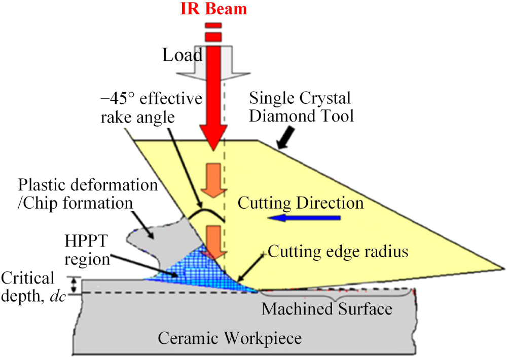
Laser-assisted cutting was recently reported to be a potential method for realizing low tool wear ductile cutting of some hard and brittle materials. Traditionally, the heat-assisted cutting techniques were applied in such a way that the heating zone was in front of the cutting tool, softening materials prior to chip formation. In 2005, Patten et al [72, 73] proposed micro laser-assisted machining (μ-LAM), as shown in figure 3, where the laser beam passes directly through the cutting tool and heats the cutting zone. After that, Ravindra et al [74] investigated the ductile mode material removal and high-pressure phase transformation in silicon during the μ-LAM process. Their results demonstrated that the optimized laser power condition resulted in a greater critical depth of cut and a nearly damage-free or cured diamond structure silicon (Si-I), similar to that of the original workpiece phase.

Figure 3. Schematic of laser-assisted cutting by directly heating the cutting zone. Reprinted from [73], Copyright 2015, with permission from The Society of Manufacturing Engineers.
Download figure:
Standard image High-resolution imageUsing alternative tool materials is another challenge. As diamond tools are prone to graphitization at high temperature, they are not suitable for carbon alloy cutting. Wei et al [75] investigated laser-assisted cutting with a sapphire tool that has high heat resistance.
4.1.3. Microstructure cutting
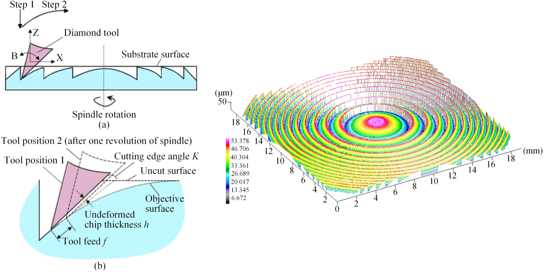
Microstructures with a high aspect ratio, such as V-grooves, pyramids, and microlens arrays, can enhance the functionality of surfaces in many ways. Such microstructured optics are used in various optical applications for imaging, illumination, or light concentration [76–79]. One example is the Fresnel lens, which can be machined by diamond turning with the tool path matching the contour of the structure. For example, the microgrooving process was performed on single-crystal Ge for fabricating infrared Fresnel lenses [80], where a sharply pointed diamond tool was used to generate the micro-Fresnel structures under three-axis ultraprecision numerical control, as shown in figure 4. By adopting a small angle between the cutting edge and the tangent of the objective surface, this method enabled the uniform thinning of the undeformed chip thickness to the nanometric range and thus provided complete ductile regime machining of brittle materials. A Fresnel lens, which has a form error of 0.5 μm and a surface roughness of 20–50 nm Ry was successfully fabricated during a single tool pass.

Figure 4. Schematic diagrams for the microgrooving process for fabricating Fresnel lenses on single-crystal Ge and a surface topography of the machined lens. Reproduced from [80]. © IOP Publishing Ltd. All rights reserved.
Download figure:
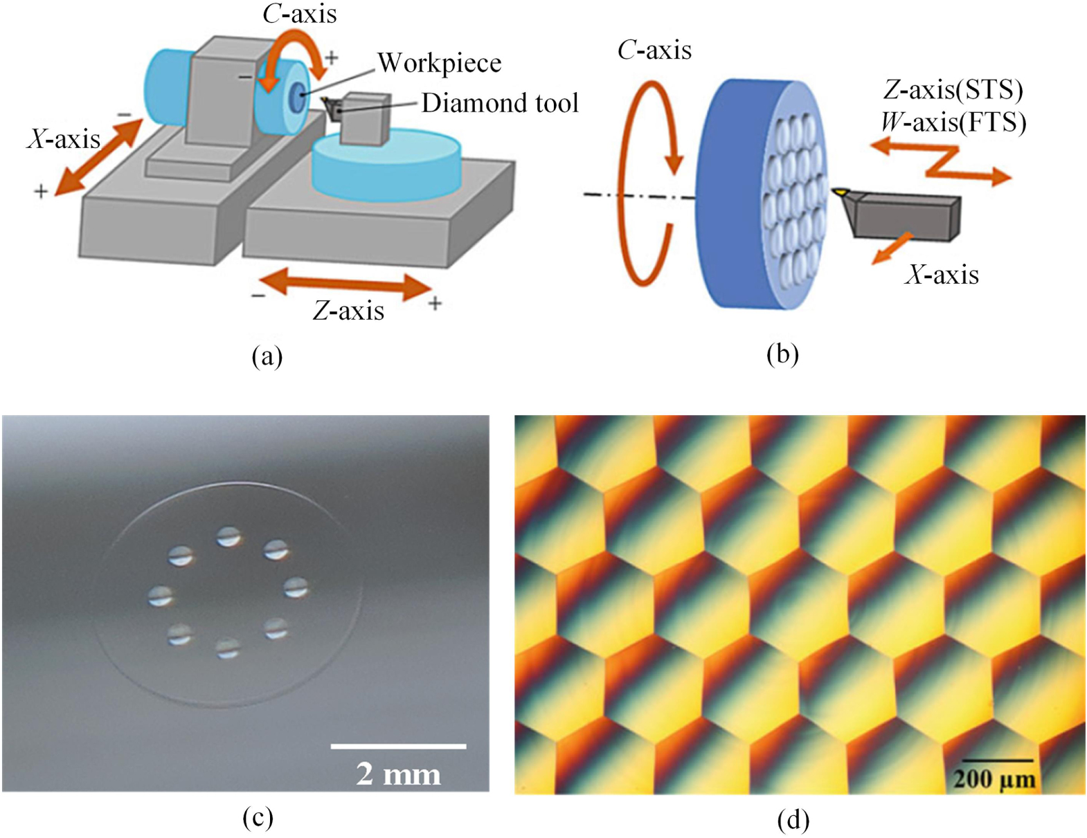
Standard image High-resolution imageAnother example of microstructure cutting on hard and brittle material is the machining for spherical and hexagonal concave microlens arrays on a single-crystal Si wafer by STS diamond turning, as shown in figure 5 [81]. The rapid fabrication of microlens arrays on the surface of single crystal Si was realized by the sectional cutting method where the follow-up error of the tool servo was suppressed. Microlens arrays with a form error of ∼300 nm peak-to-valley (PV) and a surface roughness of ∼6 nm Sa were successfully fabricated.

Figure 5. Spherical and hexagonal microlens arrays on a single-crystal Si wafer machined by slow tool servo diamond turning. Reprinted from [81], Copyright 2017, with permission from Elsevier.
Download figure:
Standard image High-resolution image4.1.4. Ultrasonic-vibration assisted cutting
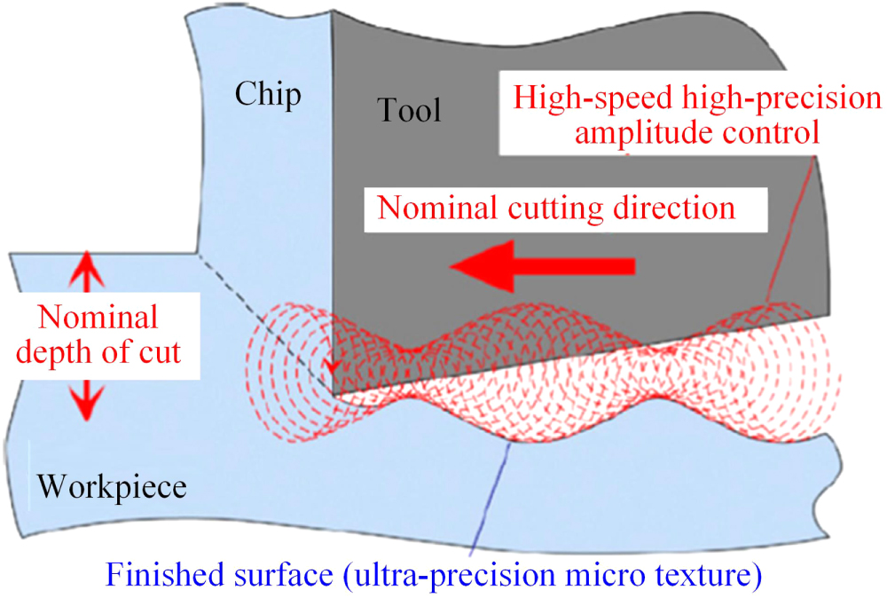
Hardened steel is a common die material developed for molding plastic and glass optical elements. However, conventional diamond cutting is not applicable to steel materials due to the extremely severe chemical tool wear [82]. In the last few decades, ultrasonic vibration cutting technology has been successfully applied to difficult-to-cut materials [83, 84]. Shamoto et al [85] proposed the elliptical vibration cutting (EVC) method, as shown in figure 6. The feasibility of cutting steel with diamond tools was verified by applying EVC. Moreover, the vibration amplitude of the EVC is actively controlled while machining. Thus, the depth of cut can be changed rapidly just like using a fast tool servo (FTS). This technology combines the advantages of EVC and FTS, which enables fabrication of micro/nanostructures on difficult-to-cut materials [86]. The EVC system developed was applied to sculpture arbitrary micro-/nanostructures by vibration amplitude control. Subsequently, a nanometer-scale sculpture was fabricated on a hardened steel surface. Figure 7 shows an example of a machined angle grid surface with a height of 1 μm and a wavelength of 150 μm on hardened steel [87].

Figure 6. Amplitude control sculpturing method in elliptical vibration cutting. Reprinted from [85], Copyright 1994, with permission from CIRP.
Download figure:
Standard image High-resolution image
Figure 7. Machined angle grid surface with a height of 1 μm and a wavelength of 150 μm. Reproduced from [87]. CC BY 3.0.
Download figure:
Standard image High-resolution image4.1.5. Fly cutting of large crystals
Fly cutting is an intermittent cutting process in which a diamond tool is mounted to the end of a spindle to intermittently cut a workpiece [88–91]. This process has important applications in the production of large flat surfaces. Figure 8 is an example of fly cutting of potassium dihydrogen phosphate (KDP) crystal which has excellent nonlinear optical properties [4]. Potassium dihydrogen phosphate crystal is a typical soft, brittle material which has poor processing properties, such as easy deliquescence and mechanical anisotropy [92]. This makes it one of the most difficult to cut materials. Ultraprecision fly cutting has proven to be an effective processing method to fabricate large-sized KDP crystals. The flatness of large KDP crystals was machined within 500 nm, and the surface roughness reached 1 nm Ra [93–95]. Recently, the fly cutting method has also been equipped with a slow FTS to fabricate hybrid structural surfaces on freeform surfaces [96].

Figure 8. Schematic of the processing of large-aperture KDP crystal by fly cutting. [4] 2016. Reprinted by permission of the publisher (Taylor & Francis Ltd, http://tandfonline.com).
Download figure:
Standard image High-resolution image4.1.6. Diamond turning of roll-to-roll imprinting molds
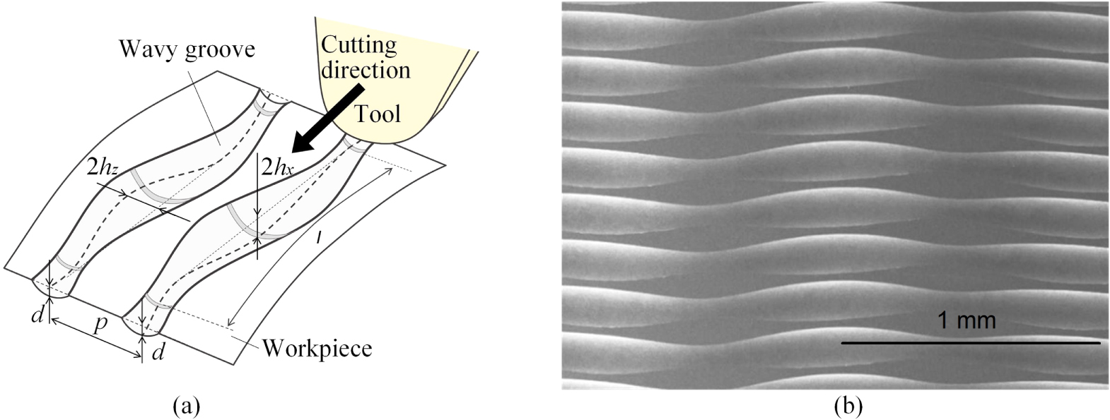
Diamond turning of high-precision molds is a vital process for the roll-to-roll resin imprinting process used in fabricating subwavelength gratings [97–102]. Jones et al [103] presented a focused-ion-beam fabricated diamond tool for producing submicron structures through a roll-based mastering method. Burr formation was minimized, and the surface quality of the product was improved by optimizing the tool shape and the microcutting conditions. Liu et al [104] suggested that a higher cutting speed was the most critical factor influencing the mold accuracy. The experimental result demonstrated that through the strict control of cutting parameters, diamond turning was an effective approach for ensuring the continual mass production of subwavelength gratings. Moreover, Terabayashi et al [105] proposed a method for machining two-directional wavy microgrooves by using a slow tool servo (STS) system. As shown in figure 9, microgrooving experiments using a two-axis STS system were conducted on cylindrical oxygen-free copper roller molds to machine various wavy microgrooves. The resulting form accuracy on the roll mold was at the ∼1 μm level and surface roughness was at the ∼10 nm level. The machined roller mold was used for ultraviolet resin imprinting, and high-precision replication of the two-directional wavy structures was realized. These structures are very useful for reducing fluid drag.

Figure 9. Slow-tool-servo turning for two-directional wavy microgrooves. Reproduced with permission from. Reproduced with permission from [105].
Download figure:
Standard image High-resolution image4.2. Ultraprecision grinding
Ultraprecision grinding is primarily used to generate high-quality, functional surfaces made of difficult-to-machine materials, such as hard and brittle materials. Through the multipoint cutting actions of ultrafine abrasive grains, ultraprecision grinding can generate parts with high surface finish, high form accuracy, and high surface integrity at reduced tool wear, compared to diamond cutting.
4.2.1. Ductile mode grinding
The fracture toughness of hard and brittle materials, such as glass, is very small, only 10−2–10−3 of the metal materials [106]. Therefore, cracks appear easily during the grinding of hard and brittle materials. In recent decades, it has been established that the ultraprecision machine enabling an extremely small feed rate can achieve ultraprecision mirror surface grinding, which is similar to the grinding of metal materials. Thus, the transition from brittle-to-ductile material removal is considered to be of great importance for ultraprecision grinding. Until now, intensive research efforts have been focused on the ductile grinding of a variety of hard and brittle materials, such as Si [107], silicon carbide (SiC) [108], and optical glasses [109, 110].
The critical depth of cut (critical chip thickness in a 3D model) for ductile-brittle transition is the most critical parameter to produce a ductile ground surface. Ductile grinding of hard and brittle materials requires a maximum chip thickness not exceeding the critical value for crack initiation. In most cases, the critical chip thickness in grinding is different from that in cutting due to the significant difference in the edge geometries between a diamond cutting tool and abrasive grains. Several investigations about the critical depth of cut brittle materials have been conducted by indentation and scratching. A simple equation was developed for the calculation of the critical depth of cut in grinding in terms of material properties [111]

where E is Young's modulus, Kc is fracture toughness, and H is hardness. The critical chip thickness can be estimated from equation (1).
To achieve ductile mode grinding, a diamond wheel having fine/ultrafine grains is critical [112]. Essentially, truing/dressing the wheel surface to make a uniform protrusion of grains is a key point for ductile mode grinding.
4.2.2. Grinding kinematics
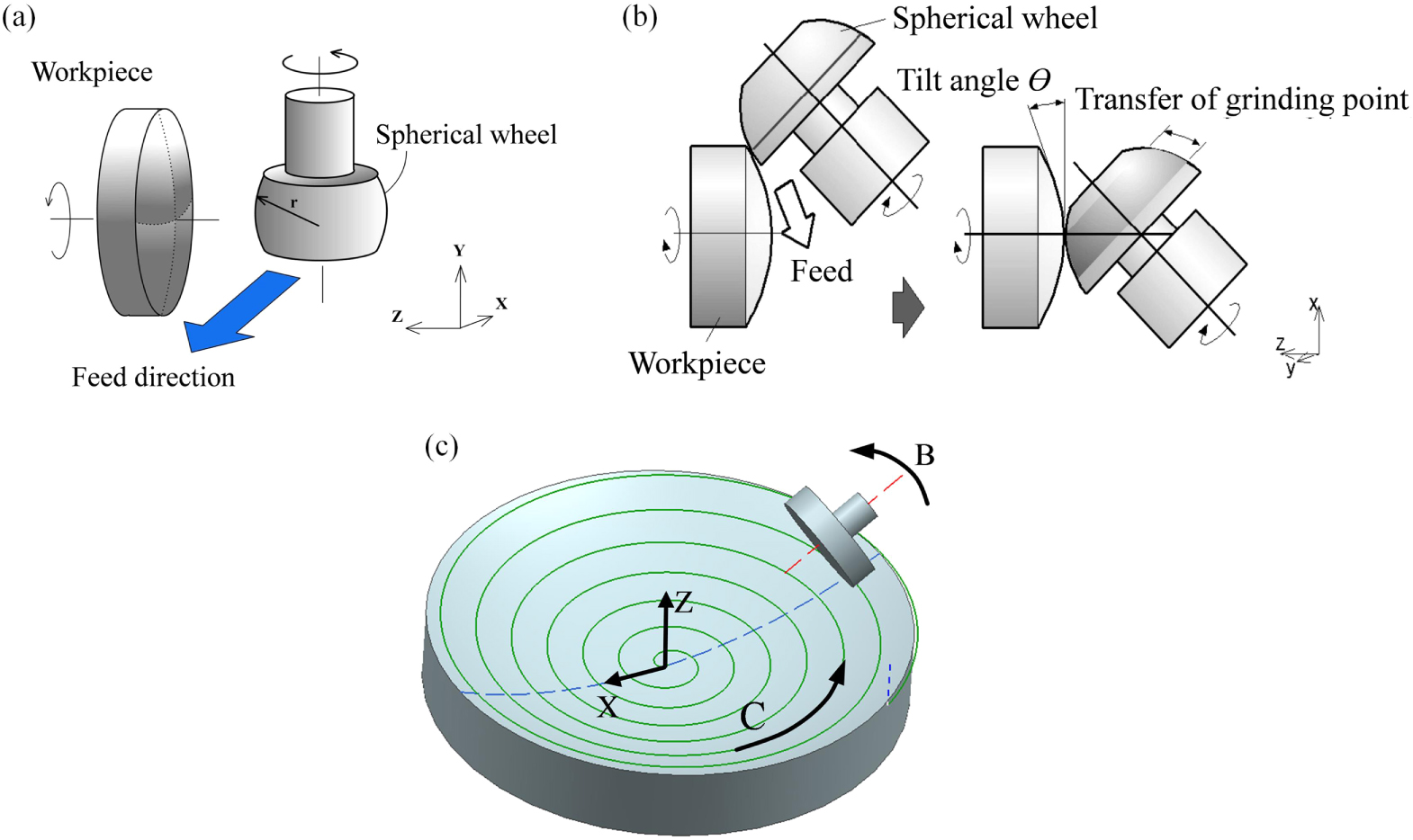
In recent years, several grinding kinematics, including cross-grinding, parallel grinding, and wheel-axis adaptive grinding, have been developed for the precision grinding of curved surfaces [113–115]. Cross-grinding is the most common grinding technique for large convex surfaces. As shown in figure 10(a), the rotational direction of the workpiece and the cutting direction of the wheel are perpendicular at the grinding point. The wheel wear is concentrated at the contact point. Therefore, it is difficult to obtain a high form of accuracy when the workpiece is very hard and the size is large. Parallel grinding employs an arc-shaped grinding wheel, where the grinding spindle is tilted with respect to the workpiece axis [113]. As shown in figure 10(b), the grinding point moves along the grinding wheel, thus the wheel wear could be dispersed over a large area, which is helpful for improving form accuracy. However, the form accuracy of the grinding wheel must be high for parallel grinding, which is a critical issue.

Figure 10. Relative motion between wheel and workpiece: (a) cross-grinding method, (b) parallel grinding method, and (c) wheel-axis adaptive grinding. [116] 2016 © Springer-Verlag London. With permission of Springer.
Download figure:
Standard image High-resolution imageWheel-axis adaptive grinding means the wheel axis always changes to keep the wheel normal to the workpiece surface [116]. As shown in figure 10(c), the grinding point remains constant during grinding as a result of the tool-axis rotation. This grinding mode has a very low requirement of wheel form accuracy. However, wheel wears rapidly at the fixed grinding point, which introduces a gradually increased form error on the ground surface.
4.2.3. In-process dressing technologies
In order to reduce the surface roughness and SSD on ground wafers, grinding wheels with smaller diamond grains are desirable. However, when the size of diamond grains decreases to micron scale with a high concentration, it is very difficult for the wheel to maintain sufficient self-dressing ability [117].
To solve this problem, the electrolytic in-process dressing (ELID) grinding method was proposed. The ELID continuously exposes new sharp abrasive grains by dissolving the bond material (mainly cast iron) around the abrasive grains [118]. As shown in figure 11, the wheel surface had good conductivity at the predressing stage. The conductivity of the wheel surface was reduced with the growth of the oxide layer thickness. However, the oxide layer became worn along with the grinding action. The wear of the oxide layer caused an increase in conductivity of the wheel surface. Thus, the electrolysis could be restarted and the oxide layer regenerated. By this manner, the protrusion of the grains remains constant during grinding.

Figure 11. Principle of ELID grinding. Reproduced with permission from [118].
Download figure:
Standard image High-resolution imageIn 1985, ELID grinding of ceramics was reported using metal-bond diamond wheels with grain sizes smaller than 30 μm [119]. Afterward, the ELID technique was further improved. In 1995, ELID grinding experiments on silicon wafers were conducted with a 5 nm grain size iron-bonded diamond grinding wheel. A superfine surface with Ra 3.29 Å was successfully achieved [120]. In recent years, ELID has become an important manufacturing process for hard-to-machine materials, although several technical barriers have been reported for ELID grinding to achieve extreme precision [121]. For example, the material removal rate in ELID grinding of Si wafers is low compared to conventional wafer grinding. As the wheels are dressed during the grinding process, the wheel wear must be precisely compensated for in order to obtain high dimensional accuracy. Thus, it is difficult for ELID grinding to achieve high wafer flatness. In addition, the oxide layer on the ground surface has been reported to be a problem with ELID grinding [122].
In addition to ELID, there are a variety of other in-process dressing methods, such as electrochemical in-process controlled dressing (ECD) [123], laser dressing [124], laser-assisted dressing [125], water-jet in-process dressing [126], ultrasonic dressing [127], and electrical discharge dressing [128]. These methods all have their advantages and problems and need to be studied further prior to application in ultraprecision grinding.
4.2.4. Chemo-mechanical grinding technology
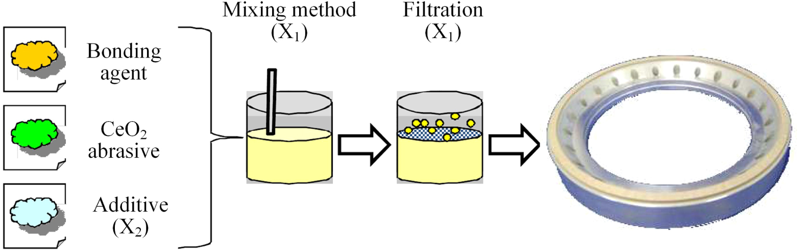
Diamond grinding induces grinding marks and SSD in the form of crystal defects and amorphous layers [129]. Those defects can be removed in the subsequent CMP process [130]. As an alternative, Zhou et al [131] proposed the chemo-mechanical-grinding (CMG) process, which combines the advantages of both grinding and polishing. The CMG is a fixed abrasive process integrating chemical reaction and mechanical grinding into one process and shows advantages against CMP in efficiency, geometric controllability, and waste disposal. Figure 12 shows the manufacturing process of the CMG wheel [132]. The experimental results indicated that the CMG process could achieve supersurface finishing comparable to that obtained from CMP by decreasing the wheel abrasive hardness and introducing chemical reactions with the workpiece surface [133, 134]. The application of CMG in the processing of crystalline materials, such as silicon [135], quartz glass [136], and sapphire [137] have been reported. A major issue in CMG is the relatively low material removal rate.

Figure 12. Manufacturing process of the CMG wheel. Reprinted from [130], Copyright 2012, with permission from Elsevier.
Download figure:
Standard image High-resolution image4.2.5. Microstructure grinding
Microstructures on nonferrous metals can be machined by single-point diamond machining [6]; grinding is preferred for processing hard materials, especially ceramics such as fused quartz glass, SiC, and tungsten carbide (WC). A number of such grinding processes have been developed in recent years. For example, Guo et al [138] proposed an ultrasonic-vibration-assisted grinding technique to fabricate microstructured surfaces. The experimental results indicated that the introduction of ultrasonic vibration was able to both improve the surface finish and the edge sharpness of the microstructures. Micro-V-groove arrays and pyramid arrays were successfully machined on binderless WC as well as SiC. The edge radius of the V-grooves and pyramids was less than 1 μm [139].
Figure 13 shows the schematic of grinding microgrooves [140]. The flat diamond grinding wheel is trued into a V-shaped microtip. The wheel moves horizontally along the cutting direction. Yin et al [141] developed a V-groove grinding process by applying ELID and microtruing operations. The minimum wheel tip radius of 8.2 μm was achieved by microtruing the grinding wheel in a diameter of 305 mm. Finally, a corner radius of V-groove ranging from 15 to 25.8 μm could be realized on a Ge surface. The grinding method developed was used in the fabrication of a large Ge immersion grating element for the SUBARU Telescope.

Figure 13. Schematic of microgrinding of microgroove. [140] © Springer Nature Singapore Pte Ltd, 2018. With permission of Springer.
Download figure:
Standard image High-resolution image4.2.6. Grinding for large optics
The next generation of ground-based telescopes requires hundreds of meter-scale, off-axis reflective mirrors. To fulfill the fabrication demands, the Cranfield BoX™ grinding machine was developed to provide meter-scale grinding capability for optics at high material removal rates while minimizing levels of SSD [142–145]. The high loop stiffness of the BoX™ machine was demonstrated by the absence of edge roll-off and chipping, as well as the microlevel SSD layer. In the grinding of the European extremely large telescope 1.45 m freeform ZERODUR® segments, an rms form deviation of <1 mm for error-compensated grinding with a surface roughness of between 100 and 200 nm Ra was achieved [146].
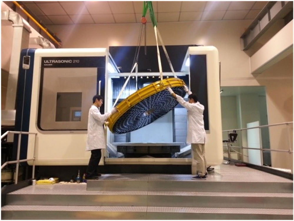
Zhang et al [116] developed an ultrasonic-vibration-assisted, fix-point grinding technology. In-process compensation of surface form error was developed based on the wheel wear prediction and modification of the tool path. Using the grinding strategies developed, a 2 m SiC mirror blank, as shown in figure 14, was ground to a form accuracy of 2 μm in rms.

Figure 14. Mounting of a 2 m SiC mirror blank onto a machining center for surface grinding. [116] 2016 © Springer-Verlag London. With permission of Springer.
Download figure:
Standard image High-resolution image4.3. Corrective polishing
4.3.1. Computer-controlled optical surfacing
The form accuracy of the workpiece finished by cutting and grinding is determined by the high-precision spatial motion trajectory of the ultraprecision machine tools. In theory, the accuracy of a workpiece surface cannot exceed that of the machine tools.
In the 1970s, Rupp proposed the CCOS process [147]. As shown in figure 15, a polishing tool with a smaller diameter than the workpiece is controlled to pass through the workpiece surface and polish off a certain amount of material at each individual point.

Figure 15. Schematic diagram of the CCOS.
Download figure:
Standard image High-resolution imageAs shown in figure 16(a), the feed speed along the tool path is purposefully changed to control the dwell time (polishing time) at each point [149]. The polishing tool is controlled to ride on the high regions to cut off the peaks, while skipping the low regions without removing the material there. Therefore, a low frequency surface error can be corrected, as shown in figure 16(a). Theoretically, the amount of material removed is determined by the local dwell time and tool impact function (TIF). The TIF means the spatial removal amount of polishing tool in unit time. The material removed is a convolution of the removal function and the dwell time, given as follows:

where H(x, y) is the desired removal function, R(x, y) is the TIF per unit time, and D(x, y) is the dwell time function. As shown in figure 16(b), the high points in the polishing tool covered area, which suffer greater pressure, were removed first so that the high frequency surface errors were eliminated.

Figure 16. Figuring and smoothing through CCOS. Reprinted from [148], Copyright 1987, with permission from Elsevier.
Download figure:
Standard image High-resolution imageComputer-controlled optical surfacing uses an iterative approach to achieve the desired surface precision. First, the error distribution of the workpiece surface is obtained by accurate measurement. Then, the local dwell time of the polishing tool on the workpiece is calculated. After that, the polishing tool is controlled to correct the local surface errors on the workpiece surface. By sufficient rounds of error correction, extremely high-precision surfaces with a smooth surface could be achieved even using low-precision machine tools [148].
One of the early applications of the CCOS technology is the manufacture of the HST [150], and today CCOS is being widely used in the manufacture of high-precision large aspheric optical surfaces.
In CCOS, the polishing tool makes the physical contact and removes material from the workpiece. Thus, tool development is an especially complex task, especially for aspheric (or freeform) optics manufacturing. Local curvatures of an aspheric surface vary as a function of position on a workpiece; however, the CCOS uses a rigid polishing tool whose shape cannot change during polishing. When polishing a large aspheric surface, a rigid polishing tool cannot follow the curvature changes at different areas of the surface, resulting in the inconsistency of material removal rate and low efficiency of surface error convergence. In order to improve the performance of a rigid polishing tool, several flexible contact polishing methods were proposed to maintain good contact with the workpiece surface. These methods include stressed-lap polishing [151], bonnet polishing [152], and rigid conformal (RC) tool polishing [153], which will be reviewed as follows.
4.3.2. Stressed-lap polishing
As early as 1984, Angle et al [154] proposed that the polishing tool should be actively deformed in order to reproduce the subaperture shape of the aspheric mirror corresponding to the pad position on the mirror surface, as shown in figure 17 [156]. Based on this concept, several stressed laps were designed to change their shape in-process to coincide with the mirror surface during polishing [157–160]. Figure 18 shows one design of a stressed lap in which the deformation of the pad surface is achieved by drawing steel wire using a servo motor [155]. Stressed-lap polishing has significant advantages in the polishing of superlarge astronomical telescopes. One example is that an 8.4 m diameter primary mirror in the Giant Magellan Telescope (GMT) project was processed by the Steward Observatory Mirror Lab at the University of Arizona [161]. Stressed-lap polishing with a diameter of 1 m was developed. After polishing, full surface roughness and form accuracy reached 20 nm Ra and less than 1 μm, respectively [162].

Figure 17. The schematic diagram of stressed-lap polishing technology. Reproduced with permission from [155].
Download figure:
Standard image High-resolution image
Figure 18. Top view of the stressed lap. Reproduced with permission from [155].
Download figure:
Standard image High-resolution image4.3.3. Bonnet polishing
As shown in figure 19, the first principle of bonnet polishing is to use a flexible air bonnet as the polishing tool [163]. The air pressure in the air bonnet can be adjusted in real time, and the outside of the air bonnet is covered with a layer of polishing cloth. The flexible air bonnet coincides with the workpiece surface.

Figure 19. The schematic diagrams of the 'precession' motion in bonnet polishing.
Download figure:
Standard image High-resolution imageThe second principle of bonnet polishing is to use a kind of motion called 'precession,' which is different from the 'rotation' and 'translation' of a traditional polishing tool [164–166]. The precession motion is divided into two parts: (1) the air bonnet rotates around the normal direction of the tool and (2) the air bonnet rotates around the normal direction of the workpiece at a certain angle, as shown in figure 18. Due to the precession motion, bonnet polishing can homogenize the motion trajectory, thus improving the machined surface roughness.
Bonnet polishing is a kind of flexible polishing, which is characterized by high determinacy of TIF and high convergence efficiency. However, due to the use of a spherical air bonnet, the contact area with the workpiece is small; and the material removal efficiency is low.
4.3.4. Rigid conformal lap polishing
In 2009, Kim and Burge proposed a rigid conformal polishing tool that conforms to the aspheric shape yet maintains stability to provide natural smoothing for high spatial-frequency errors on the workpiece [167–169]. The tool uses an elastic rubber paste called Silly-Putty® as the deformed layer of the polishing tool, as shown in figure 20. Silly-Putty is an organosilicon polymer and a nonlinear viscoelastic non-Newtonian fluid [170]. The fluid has both flexibility and rigidity for different time scales. Under long-term stress, it shows the fluidity of liquid; under high-frequency stress, it shows the rigidity of solid. Therefore, the rigid conformal polishing tool has not only the ability of a flexible polishing tool for a nonspherical surface but also the smoothing effect of a rigid polishing tool.

Figure 20. Three-dimensional schematic of rigid conformal lap structure. Reproduced with permission from [153]. © 2010 Optical Society of America.
Download figure:
Standard image High-resolution imageCompared with CCOS methods, rigid conformal lap balances the advantages and disadvantages of various processing methods. Therefore, it has various advantages, such as excellent TIF stability, high material removal rate, and good physical smoothing ability. Moreover, rigid conformal lap can provide a supersmooth surface finish with <1 nm rms. This may eliminate the need for the final touch-up step for a supersmooth surface finish. Because of these competitive advantages, the rigid conformal lap polishing is very suitable for processing large aperture aspheric mirrors with high steepness and large deviation. The Steward Observatory Mirror Lab of the University of Arizona successfully applied this technology to the GMT 8.4 m primary mirror fabrication [171].
4.3.5. Magnetorheological finishing
The aforementioned polishing methods made changes to the polishing tool but did not change the polishing fluid or abrasives, thus it was difficult to ensure long-term stability of the TIF because of the poor consistency of particle concentration in polishing regions. In order to solve this problem, MRF was developed.
Magnetorheological finishing was originally proposed by Kordonski et al in the former Soviet Union [172]. The working principle of MRF is illustrated in figure 21 [173]. The magnetorheological fluid is composed of base fluid, surfactant, magnetic particles, and polishing particles. Magnetorheological fluid flows out of the nozzle and moves along the polishing wheel to the top area. The viscosity of magnetorheological fluids increases instantaneously, becoming viscoplastic Bingham medium under the action of a high-intensity gradient magnetic field. When the Bingham medium passes through the narrow gap formed by the workpiece and the polishing wheel, it generates a great shear force at the contact area, thus removing the surface material of the workpiece.

Figure 21. Mechanisms of MRF polishing and its material removal mechanism. Reproduced with permission from [173].
Download figure:
Standard image High-resolution imageMagnetorheological finishing is a deterministic polishing process because the polishing tool will not dull or wear [174–178]. The shape, the size, and the hardness of the flexible polishing belt can be controlled by adjustment of the magnetic field intensity at the polishing zone. Therefore, the material removal consistency of MRF is greatly improved compared with CCOS.
Figure 22 is the TIF shape of the MRF, which looks like a bullet [179]. Such a TIF has only one peak value and is very helpful for the convergence of surface error. However, the TIF of MRF is very small compared with traditional large polishing tools. Therefore, the material removal rate is low and the processing time of MRF is bound to be very long for large-aperture optical surfaces.

Figure 22. The tool impact function of MRF. Reproduced with permission from [179]. © 2011 Optical Society of America.
Download figure:
Standard image High-resolution image4.3.6. Ion beam figuring
The aforementioned polishing methods are all contact processes. The polishing tools exert a certain degree of pressure on the workpiece surface, which leads to print-through of the structure of a light weighted mirror [180]. Moreover, when the polishing tool moves to the mirror edge, the polishing area becomes smaller and the pressure increases, which inevitably leads to the edge roll-off phenomenon [181].
As a noncontact and nonmechanical process, IBF has been successfully applied in the polishing of space mirrors since the 1970s [182, 183]. Figure 23 shows the working principle of IBF [184]. IBF is a method of bombarding high-energy ions (generally argon ions) into the machined surface and removing materials by physical sputtering at the atomic level. One of the main advantages of IBF is the contactless nature of an ion beam as a polishing tool, which eliminates the edge roll-off effects of mechanical tools. Because the energy distribution of an ion beam can be accurately controlled, excellent stability of atomic-level removal can be achieved [185–187].

Figure 23. Schematic of the principle of ion beam figuring. [184] 2015 © Springer-Verlag London. With permission of Springer.
Download figure:
Standard image High-resolution imageThere are, however, a few trade-offs to these benefits. The deterministic removal of this method depends heavily on the stability of the ion source and the environmental stability of the vacuum chamber. The material removal efficiency of IBF is very low compared to mechanical methods due to atomic-level material removal characteristics.
4.4. Supersmooth polishing
4.4.1. Elastic emission machining
EEM was first proposed as a polishing method by Mori et al about 40 years ago [188]. EEM is a noncontact machining method that involves passing a flow of fine powder particles in pure water across the workpiece surface. As shown in figure 24, the particles supplied in a flow of pure water and the topmost atoms of the work surface are chemically removed at the atomic level. Hence, the work surface can be finished without defects. In most cases, silica particles with submicron diameters are used as abrasives.

Figure 24. Schematic of atom removal process in EEM. Reproduced with permission from [189]. © American Vacuum Society.
Download figure:
Standard image High-resolution imageKanaoka [189] investigated the smoothing performance of rotating-sphere EEM for processing ULE® and ZERODUR materials for EUV optics. It was demonstrated that the rms surface roughness converged to a constant value of 0.1 nm after removal of a certain depth of material. The surface roughness can thus be reduced to 0.1 nm rms or better, fulfilling the requirements of the EUV optics.
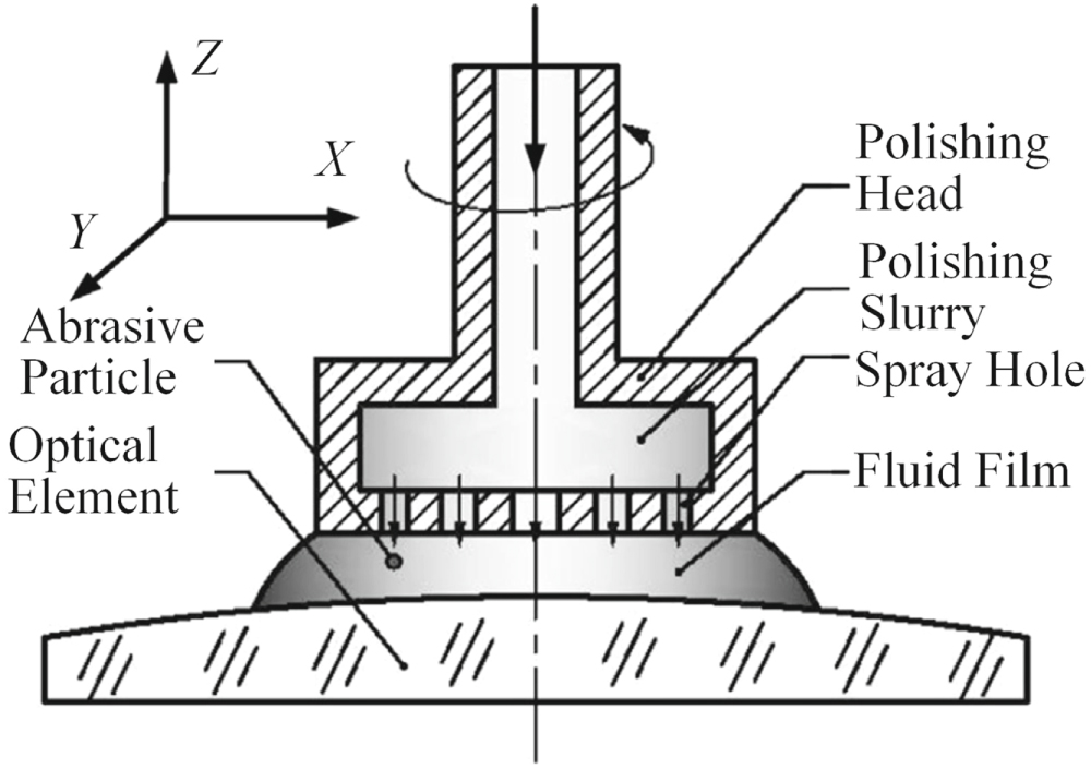
4.4.2. Microfluid jet polishing
In order to achieve supersmooth lenses for 193 nm projection lithography systems, Ma et al [190] proposed a supersmooth polishing method called MFJP, which combined the principles of float polishing, CCOS, and abrasive jet polishing. As shown in figure 25, the polishing slurry outflowed from the spray holes of the polishing head, lifting the polishing tool a certain distance through the dynamic pressure caused by the motion of the polishing slurry. The chemical reaction between the workpiece and the fine powder particles results in the removal of the topmost atoms from the workpiece surface.

Figure 25. Principle of microfluid jet polishing. Reprinted from [190], Copyright 2013, with permission from Elsevier.
Download figure:
Standard image High-resolution imageA 100 mm diameter (95% effective aperture) fused silica flat optical element was polished using the MFJP method. Testing results showed that the low-spatial form accuracy improved from 3.624 to 3.393 nm in rms, and the midspatial frequency surface roughness improved from 0.477 to 0.309 nm in rms. The high-spatial frequency surface roughness improved from 0.167 to 0.0802 nm in Rq. The power spectral density curve before and after supersmoothing uniform polishing is also shown in figure 26, in which the mid- and high-spatial frequency roughness was significantly improved; but the low-spatial surface form was not obviously changed.

Figure 26. (a) Low, (b) mid-, and (c) high-spatial frequency PSD data. Reprinted from [190], Copyright 2013, with permission from Elsevier.
Download figure:
Standard image High-resolution image5. On-machine measurement (OMM) and compensation
For the form error correction process, the precise measurement of the machined surface is an essential step. Metrology is the most important supporting technology for ultraprecision manufacturing. Without ultraprecision metrology, there will be no advance in the precision level of manufacturing. Typical surface metrology methods for ultraprecision surfaces include contact/noncontact profilometer, laser interferometer, white light interferometer microscope, and atomic force microscope. However, most of the above-mentioned measurement methods are off-machine methods. Because of the remounting process, off-machine measurements reduce manufacturing efficiency and may cause measurement error due to workpiece remounting and/or environmental changes. In order to solve these problems, on-machine metrology and error compensation based on the measurement result is expected.
There are several methods of realizing OMMs. A touching probe, i.e. the so-called linear variable differential transformer, is always installed on a commercial diamond turning machine. Other methods include laser and chromatic confocal probes, which are noncontact and nondestructive methods for surface measurement. For example, Chen et al [191] presented an OMM approach using a sapphire microprobe of 0.5 μm in radius for the grinding of tungsten carbide aspheric molds. The overall form error after grinding was obtained by subtracting the target form from the actual ground form. The aspheric surface had a high form accuracy of 0.177 μm after three compensation cycles. Li et al [192] proposed an OMM system based on capacitive displacement sensors for high-precision optical surfaces. A 92% of full aperture measurement of a spherical aluminum mirror with a diameter of 300 mm was carried out, and the complete measurement of the form error required only 5 min. Zou et al [193] developed a chromatic confocal sensor to achieve noncontact measurement with nanometer-level accuracy for an ultraprecision turning machine and is capable of reconstructing the 3D surface topography of flat, spherical, and aspheric surfaces. Li et al [194] integrated a dispersed reference interferometer on an ultraprecision turning machine. Yan et al used a white-light interferometer for nanometer level precision on-machine profiling of curved diamond cutting tools [195]. Both theoretical and experimental investigation was conducted to prove the validity and effectiveness of the proposed calibration methodology. In addition, as shown in figure 27, Yu et al [196] proposed an OMM system using two optical probes to rapidly reconstruct the surface form from the radial and axial directions. Thus, a two-step compensation strategy to generate a modified tool path was developed. The results show that the OMM system and compensation strategy were effective for improving the form accuracy while simultaneously enhancing the machining efficiency.

Figure 27. Schematic of the two-probe measurement system mounted on an ultraprecision lathe. Reproduced with permission from [195].
Download figure:
Standard image High-resolution imageThe error compensation strategy is a very important issue. For example, in diamond turning, a typical machining cycle consists of three steps: programming to generate tool paths, tool alignment step for tool-workpiece alignment, and machining for surface generation. A number of factors cause workpiece form errors during each step of the process. In a conventional process flow, the form error is corrected by using feedback correction, thus only a specific error factor is compensated for based on the experimentally measured form error. The machining-measurement cycle must be repeated many times because the form error decreases gradually in each cycle; and it is extremely difficult and time-consuming to reduce the form error completely.
Nagayama et al [197] proposed a new process flow which includes error correction and prediction, as shown in figure 28. The flow is composed of four steps: (1) program optimization, (2) tool alignment error correction, (3) machining error modification, and (4) form error prediction. In this flow, all of the main error factors are optimized in Steps (1), (2), and (3) based on error analysis; and the form error of the finished surface is predicted in step (4). All of the error corrections are carried out, and the finished form error is predicted before machining. In this way, a very high form accuracy can be obtained in a single cycle. Figures 29(a) and (b) show the simulation and experiment results of form errors under different conditions. In the simulation, the form error was predicted to be reduced by 80% with correction steps (1), (2), and (3), compared to the case of machining without any corrections. The results of the experiment agree well with the simulated results. Figure 29(c) shows the 3D topography of the surface machined after all of the correction steps. A 10 nm level sinusoidal wave grid was successfully fabricated on a single crystal Si wafer by STS turning, and the form accuracy was 8 nm PV [196].

Download figure:
Standard image High-resolution image
Figure 29. Results of simulation and experiment of form errors under different conditions of correction/prediction machining. Reproduced from [196]. CC BY 4.0.
Download figure:
Standard image High-resolution image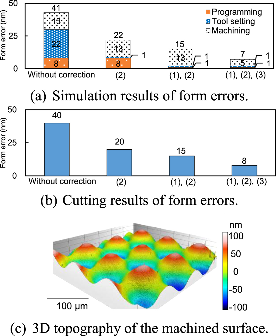
6. Summary and outlook
Improving form accuracy and surface finish is the permanent pursuit of high-value-added manufacturing technologies. With the demands of the next generation EUV lithography, space optics and laser fusion technology, ultraprecision machining technologies are now stepping from the nanometer scale towards the atomic scale. In the past decades, remarkable advances have been achieved in the area of high-precision manufacturing technologies based on the significant developments in machine building technology, tooling technology, measurement and control technologies. Future R&D issues towards extreme precision manufacturing can be summarized as follows.
- (1)Material removal mechanisms at the atomic scaleThe theoretical clarification of the basic principles in the material removal process at the atomic level is essential for optimizing existing manufacturing technologies and developing new technologies. In the early 1990s, Japanese scholars used extremely sharpened single-crystal diamond tools to investigate experimentally the minimum chip thickness for metal cutting and demonstrated that a cutting thickness of 1 nm was possible. Cutting experiments in scanning electron microscopes and nanoindentation tests have been also used to clarify the nanoscale phenomena of machining. Such fundamental research will be still important in the future for challenging the ultimate dimensional accuracy of ultraprecision cutting. In recent years, molecular dynamics simulation has been applied to study the nanometric and atomic scale cutting, grinding, and polishing processes, which has made it easier for us to reveal a material removal mechanism and investigate the machinability of various materials at small scales.
- (2)Surface/subsurface evaluation for extreme-precision machiningWith the development of high-resolution and high-reliability displacement sensors, noncontact OMM technology will have a major breakthrough in the future, which will enable deterministic compensation strategy of surface form errors. On the other hand, SSDs such as potential microcracks, phase transformations, and residual stresses, which cannot be directly measured from the surface, also affects the imaging quality, long-term stability, and laser-induced damage threshold of optical components. Therefore, characterization and control of subsurface properties has become one of the key issues in the optical and semiconductor manufacturing industry. It is necessary to develop integrated evaluation technologies to realize OMM, error compensation, and subsurface evaluation.
- (3)Compatibility of precision and cost-efficiency
Some ultraprecision machining technologies can achieve high-quality surface finish and surface integrity, but the processing efficiency is very low. It will be a long-term goal of researchers in the field of ultraprecision machining to explore processing methods that can improve both cost-efficiency and accuracy. To achieve this goal, a multidisciplinary approach for manufacturing R&D by interfacing manufacturing with mechanical science, physics, material science and nanotechnology is necessary. There is still a long way to go in this direction towards the industrial application of the extreme-precision machining technologies to mass production of consumer products.