

Abstract
This paper presents the efficiency tables of materials considered as emerging inorganic absorbers for photovoltaic solar cell technologies. The materials collected in these tables are selected based on their progress in recent years, and their demonstrated potential as future photovoltaic absorbers. The first part of the paper consists of the criteria for the inclusion of the different technologies in this paper, the verification means used by the authors, and recommendation for measurement best practices. The second part details the highest world-class certified solar cell efficiencies, and the highest non-certified cases (some independently confirmed). The third part highlights the new entries including the record efficiencies, as well as new materials included in this version of the tables. The final part is dedicated to review a specific aspect of materials research that the authors consider of high relevance for the scientific community. In this version of the Efficiency tables, we are including an overview of the latest progress in theoretical methods for modeling of new photovoltaic absorber materials expected to be synthesized and confirmed in the near future. We hope that this emerging inorganic Solar Cell Efficiency Tables (Version 1) paper, as well as its future versions, will advance the field of emerging photovoltaic solar cells by summarizing the progress to date and outlining the future promising research directions.
Export citation and abstract BibTeX RIS
Abbreviations
| Eff. (%) | Conversion efficiency obtained under AM1.5 illumination in percentage |
| VOC (V) | Open circuit voltage in Volts |
| JSC (mA cm−2) | Short circuit current in mili-Ampers by square centimeter |
| F. F. (%) | Fill factor in percentage |
| Eg (eV) | Bandgap in electronvolt |
| AZO | ZnO:Al |
| ITO | In2O3:SnO2 |
| Spiro-OMeTAD | 2,2',7,7'-Tetrakis[N,N-di(4-methoxyphenyl)amino]-9,9'-spirobifluorene (C81H68N4O8) |
| TBAI | Tetrabutylammonium iodide |
| EDT | 1,2-ethanedithiol |
| PTB7 | Poly[[4,8-bis[(2-ethylhexyl)oxy]benzo[1,2-b:4,5-b']dithiophene-2,6-diyl][3-fluoro-2-[(2-ethylhexyl)carbonyl]thieno[3,4-b]thiophenediyl]] ((C41H53FO4S4)n) |
| ARC | Anti-reflection coating |
| CuPc+ | Copper phthalocyanine |
| PTAA | Poly[bis(4-phenyl)(2,4,6-trimethylphenyl)amine ((C21H19N)n) |
| PCBM | [6,6]-Phenyl C61 butyric acid methyl ester (C72H14O2) |
| mp-TiO2 | Mesoporous TiO2 |
| PCPDTBT | poly[N-9'-heptadecanyl-2,7-carbazole-alt-5,5-(4,7-di-2-thienyl-2',1',3'-benzothiadiazole] ((C43H47N3S3)nC12H10) |
| PEDOT:PSS | Poly(2,3-dihydrothieno-1,4-dioxin)-poly(styrenesulfonate) |
| P3HT | Poly(3-hexylthiophene-2,5-diyl) ((C10H14S)n) |
1. Introduction
1.1. Scope of the paper
Several photovoltaic technologies have now reached the point where they are mature enough, to reach the market and the progress in their power conversion efficiencies are summarized regularly in 'Solar Cell Efficiency Tables' [1]. Crystalline and multi-crystalline Si modules are the industrial standard but amorphous-Si, Cu(In, Ga)(S, Se)2, CdTe, organic photovoltaic, dye-sensitized solar cells, etc have all been commercialized to varying degrees of success. Whilst these technologies could feasibly cover the majority of photovoltaic applications, increasing the diversity of viable photovoltaic materials will allow for greater adaptability as the technology continues to expand and develop. Additionally, most of the established platforms face challenges related to either the use of critical raw materials, toxic elements, long-term stability, conversion efficiency limitations, cost or low technological flexibility (e.g. incompatibility with flexible substrates, or transparent concepts). These are all important considerations that must be taken into account as the field begins to look towards an era of terawatt level photovoltaic power generation.
The limitations of the mature technologies encourage a continued search for new materials, as none of the established technologies represent the 'perfect' photovoltaic material. The purpose of continued exploratory research is to identify absorbers that can bring additional benefits and/or may allow the development of novel applications. New inorganic materials including chalcogenides (sulfides, selenides, tellurides), oxides, pnictides (nitrides, phosphides) and halides (mainly bromides and iodides) have proved a fruitful area of research and attracted a lot of attention. There are numerous examples published in recent years showcasing the capability of these materials to act as photovoltaic absorbers. Respectable device efficiencies have been reported for numerous cell platforms despite their typically being only limited attempts at fabrication and often with only specific groups contributing to their progresses. Several of these emerging cell structures have shown enough development to identify them as potential future technological solutions. As a result, there has been a resurgent interest from the scientific community in emerging photovoltaic solar cell absorbers, as is shown in figure 1, where the number of papers published on this topic has increased significantly in the past decade.
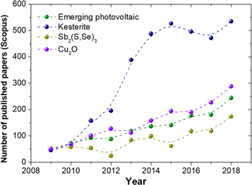
Figure 1. Number of published papers in the last 10 years referring to emerging photovoltaics, kesterite, Sb2(S, Se)3 and Cu2O (extracted from Scopus in March 2019).
Download figure:
Standard image High-resolution imageGiven the continually developing nature of the research field and the large number of emerging inorganic photovoltaic materials, this paper was conceived to collate information on the current status of the most promising materials in form of efficiency tables, collecting and summarizing the most relevant information available in the literature. This includes certified efficiencies in one of the six special centers available in the world, as well as independently measured examples with a description of the means of efficiency verification (or lack thereof). The main aim of these tables is to provide researchers working on emerging inorganic technologies with a valuable information resource by condensing all the spread information about these fascinating materials, but also to establish a forum for the discussion moving forward. It is hoped that these tables will evolve with the field and with input from the researchers in the community, informing future versions to include new champion devices or emerging technologies of note. These tables aim to support and inspire future research in the emerging inorganic solar cells.
1.2. Structure of the paper
The paper is structured in 4 sections, with the following details:
Section 1. is the present section, giving an overview of the paper, a description of its structure, an explanation about the criteria used to select the materials included in the different efficiency tables, and a description of the recommended procedures for the correct J–V in-house illuminated curve measurement, extraction of corresponding optoelectronic parameters, as well other additional devices information that the authors consider of high relevance for emerging photovoltaic technologies.
Section 2. This section contains the efficiency tables split into two categories. The first table summarizes all the world-class certifications available in the literature, and compiled by the authors. For this table we consider certified devices with efficiency higher than 5% and area larger than 0.1 cm2. Exceptions of these considerations are summarized at the end of the table. The second table collects all the devices that are non-certified but can be confirmed using specific procedure, with efficiency higher than 1% and area larger than 0.1 cm2. Exceptions of these considerations are also summarized at the end of the table. In each of these two tables, the materials are organized firstly depending on the type of compounds (oxides, chalcogenides, pnictides, halides, etc), and then in terms of complexity from less to more atoms in the structure.
Section 3. In this part of the paper, we give a brief description of new entries in terms of new efficiency records but also new materials included in the tables, with a brief review of the last and most impacting progresses reported in these technologies.
Section 4. The last section of the paper aims to bring to the scientific community a perspective review of a specific topic that the authors have identified as very timely and with high relevance. In this first edition of the efficiency tables, the authors have invited Professor Aron Walsh from Imperial College London, to review the last progresses in predictive modeling of novel materials that are not experimentally demonstrated yet, but have been identified as very promising for their future synthesis and demonstration in the laboratory. Subsequent editions of this yearly published emerging inorganic solar cell efficiency tables will include in this section an invitation of other scientists to review other topics at the forefront of the science.
1.3. Criterion for technology selection
For selecting the materials included in the Efficiency tables, the authors have defined the following criteria:
Table 1 (World class certification): fully inorganic technologies with certified materials in one of the six world class certifying centers, with efficiency higher than 5% and area larger than 0.1 cm2. Exceptions to these rules are collected separately at the end of the table.
Table 2 (Non world class certification or in house measurements): fully inorganic technologies of non-certified materials with efficiency higher than 1%, verification through external quantum efficiency (EQE) measurement, or confirmation by a second organization, and area larger than 0.1 cm2. Exceptions to these rules are collected separately at the end of the table.
Table 1. List of certified single-junction record cells under global AM1.5 spectrum (1000 W m−2) at 25 °C, including relevant optoelectronic parameters and important additional data (IEC 60904-3: 2008, ASTM G-173-03 global).
| Material | Eff. (%) | VOC (V) | JSC (mA cm−2) | F. F. (%) | Area (cm2) | Eg (eV) | Device structure | Certifying Center/Date | Comments |
|---|---|---|---|---|---|---|---|---|---|
| Sb2Se3 (substrate) | 9.2 | 0.400 | 32.6 | 70.3 | 0.26 | 1.18 | Glass/Mo/MoSe2/Sb2Se3/ZnO/AZO | CNIM (2018) | Hebei Key Laboratory of Optic-Electronic Information Materials, Hebiei University, China [2]. Substrate geometry structure incorporating core–shell nanowire approach. Absorber deposited by CSS. |
| Cu2ZnSnS4 (CZTS) | 11.0 ± 0.2 | 0.731 | 21.74 | 69.3 | 0.2339 | 1.5 | Glass/Mo/CZTS/CdS/i-ZnO/ITO/Al/MgF2 | NREL (2017) | UNSW [3]. Absorber prepared by sputtering Cu/ZnS/SnS |
| Cu2ZnSn(S0.25Se0.75)4 (CZTSSe) | 12.6 ± 0.3 | 0.513 | 35.2 | 69.8 | 0.4209 | 1.13 | Glass/Mo/CZTSSe/CdS/ZnO/ITO/Ni/Al/MgF2 | Newport (2013) | IBM [4]. Absorber prepared by spin-coating a hydrazine-based solution. |
| Cu2ZnSn(SySe1−y)4 (CZTSSe) | 12.62 ± 0.29 | 0.541 | 35.35 | 65.9 | 0.4804 | 1.13 | Glass/Mo/CZTSSe/CdS/ZnO/AZO/Ni/Al/MgF2 | Newport (2018) | DGIST [5]. Absorber prepared by sputtering Sn/Cu/Zn and reactive annealing. |
| Cu2ZnSnSe4 (CZTSe) | 11.6 | 0.423 | 40.6 | 67.3 | 0.43 | 1.0 | Glass/Mo/CZTSe/CdS/ZnO/ITO/Ni/Al/MgF2 | Newport, (2015) | IBM [6]. Absorber prepared by co-evaporation of Cu, Zn, Sn, and Se. |
| Notable exceptions | |||||||||
| Cu2O | 3.97a | 1.204 | 7.37 | 44.70 | 0.15 | 2.2 | MgF2/Al/Al:ZnO/Ga2O3/Cu2O/Au | NREL (2014) | MIT, Harvard University Cambridge and NREL [7]. Electrochemical deposition. |
| CsPbI3 | 13.58 | 1.1626 | 15.246 | 76.63 | 0.058 | NA | Al/MoOx/Spiro-OMeTAD/CsPbI3/TiO2/SnO2:F/Glass/MgF2 | NREL (2017) | NREL, University of Washington and University of Colorado [8]. Coupled quantum dots films. |
| SnS | 4.36a | 0.372 | 20.2 | 58.0 | 0.24 | 1.1 | Glass/Mo/SnS/SnO2/Zn(O, S):N/ZnO/ITO | NREL (2014) | Department of Chemistry and Biology, Harvard University, Cambridge, USA [9]. ALD deposition of absorber followed by annealing in H2S. |
| Sb2Se3 (superstrate) | 7.6 | 0.420 | 29.9 | 60.4 | 0.091b | 1.18 | Glass/ITO/CdS/Sb2Se3/Au | CNIM (2017) | Sargent Joint Research Centre, Wuhan National Laboratory for Optoelectronics and School of Optical and Electronic Information, Huazhong University of Science and Technology, Wuhan, China [10]. Vapor transport deposition. |
| Sb2(S, Se)3 | 9.9 | 0.650 | 24.07 | 63, 5 | 0.0889 | 1.53 | Glass/FTO/CdS/Sb2Se3/Spiro-OMeTAD/Au | CNIM (2019) | University of Science and Technology of China, China [11]. Hydrothermal method. |
| PbS | 9.88 | 0.635 | 21.6 | 71.9 | 0.05b | NA | Glass/ITO/ZnO/PbS(TBAI)/PbS(EDT)/Au | Newport (2015) | Wuhan National Laboratory for Optoelectronics and School of Optical and Electronic Information, Huazhong University of Science and Technology, Wuhan, China [12]. Spin coating of PbS coloidal quantum dots. |
| AgBiS2 | 6.31 | 0.450 | 22.1 | 63.0 | 0.017b | 1.3 | Glass/ITO/ZnO/AgBiS2/PTB7/MoO3 | Newport (2016) | ICFO—Institut de Ciències Fotòniques, The Barcelona Institute of Science and Technology, Barcelona, Spain [13]. Layer-by-layer spin coat deposition from nanocrystal solution. |
Note. NA—Not available. aCertified efficiency below 5%. bArea of the certified cell below 0.1 cm2 (total area).
Table 2. List of non-certified single-junction record cells under global AM1.5 spectrum (1000 W m−2) at 25 °C, including relevant optoelectronic parameters, the means of verification and important additional data (IEC 60904-3: 2008, ASTM G-173-03 global). +PC-Phtalocyanine.
| Material | Eff. (%) | VOC (V) | JSC (mA cm−2) | F. F. (%) | Area (cm2) | Eg (eV) | Device structure | Means of verification | Institutions and Comments |
|---|---|---|---|---|---|---|---|---|---|
| Zn3P2 | 6.0 | 0.492 | 14.9 | 71.0 | 0.70 | NA | ZnS/Mg/Ag:Zn3P2/Ag | No EQE results | U. Delaware [14]. CVT grown thick wafer absorber measured in AMI illumination. Measured under a simulated intensity of 87.5 mW cm−2. |
| CuSbSe2 | 4.7 | 0.336 | 26.3 | 53.0 | 0.2 | NA | Glass/Mo/CuSbSe2/ZnO/AZO | EQE, In-house | National Renewable Energy Laboratory, Golden, USA [15]. Sputtering from binary Cu2Se and Sb2Se3 targets. |
| CuSbS2 | 3.2 | 0.470 | 15.6 | 43.6 | 0.45 | 1.4–1.9 | Glass/Mo/CuSbS2/CdS/ZnO/AZO | EQE, In-house | New and Renewable Energy Research Division, Korea Institute of Energy Research, Daejeon, South Korea [16]. Sulfurization of nanoparticle inks. |
| Cu2CdSnS4 | 1.1 | 0.383 | 12.4 | 23.0 | 0.16 | 1.41 | Glass/Mo/CCdTS/CdS/ZnO/AZO/Ag | EQE, In-house | NTU [17]. Absorber prepared by spin-coating using 2-methoxyethanol-based solution |
| Cu2ZnSnSe4 | 11.8 | 0.463 | 38.3 | 66.3 | 0.522 | 1.05 | Glass/Mo/CZTSe/CdS/ZnO/ITO/Ag/MgF2 | EQE, in-house, measured in two centers | IREC, Spain; AIST, Japan; University of Barcelona, Spain; Martin-Luther-Universitat Halle-Wittenberg, Germany [18]. Sputtering of metallic precursors and reactive annealing. Ge doping (less than 0.5%). |
| Cu2BaSnS4 (substrate) | 1.7 | 0.698 | 5.3 | 46.9 | 0.2 | 2.01 | Glass/Mo/CBaTS/CdS/ZnO/ITO/Al | EQE, In-house | Central South University, UNSW, Shen Zhen University, Xiamen University [19]. Absorber prepared by spin-coating using a 2-methoxyethanol-based solution. |
| Cu2BaSnS4 (superstrate) | 2.0 | 0.933 | 5.1 | 42.9 | 0.2 | 2.04 | CdS:O/CdS/ZnO/AZO | EQE, In-house | The University of Toledo [20]. Absorber prepared by sputtering method. |
| Cu2FeSnS4 | 3.0 | 0.610 | 9.3 | 52.0 | 0.1 | 1.5 | ITO/Cu-NiO/CFeTS/Bi2S3/ZnO/Al | EQE, In-house | Indian Association for the Cultivation of Science [21]. Absorber prepared by SILAR method. |
| Cu2CdSn(S0.xxSe0.yy)4 | 2.8 | 0.356 | 18.8 | 41.6 | 0.405 | 1.55 | Glass/Mo/CCdTSSe/CdS/ZnO/ITO/Al | EQE, In-house | Changchun Institute of Applied Chemistry, Chinese Academy of Sciences [22]. Absorber prepared by spin-coating an ethanol, butyldithiocarbamic acid, and thioglycolic acid -based solution. |
| Cu2BaSn(S0.xxSe0.yy)4 | 5.2 | 0.611 | 17.4 | 48.9 | 0.425 | 1.55 | Glass/Mo/CBaTSSe/CdS/ZnO/ITO/Ni/Al | EQE, In-house | Duke University, IBM [23]. Absorber prepared by co-sputtering using Cu, Sn, and BaS. |
| Cu2ZnGe(S0.xxSe0.yy)4 | 6.0 | 0.617 | NA | NA | 0.25 | 1.47 | Glass/Mo/CZGeSSe/CdS/ZnO/AZO/Ni/Al | EQE, In-house | ZSW, CNRS [24]. Absorber prepared by doctor-blade coating a DMF-based solution. |
| Cu2ZnGeSe4 | 7.6 | 0.558 | 22.8 | 59.0 | 0.5 | 1.36 | Glass/Na-barrier/Mo/CZGeSe/CdS/ZnO/AZO/Ni/Al | EQE, In-house | CNRS, IMEC [25]. Absorber prepared by sputtering of Cu and Zn, and e-beam evaporation of Ge. |
| Ag2ZnSnSe4 | 5.18 | 0.504 | 21.0 | 48.7 | 0.45 | 1.35 | FTO/AgZTSe/MoO3/ITO/Ni/Al | EQE, In-house | IBM, UCSD [26]. Absorber prepared by coevaporation of Ag, Zn, Sn, and cracked Se. |
| Cu2(Zn0.6Cd0.4)SnS4 | 11.0 | 0.650 | 25.5 | 66.1 | 0.22 | 1.38 | Glass/Mo/CZCdTS/CdS/ZnO/ITO/Al/MgF2 | EQE, in-house | University of New South Wales, Australia; National Renewable Energy Laboratory, United States; Central South University, China [27]. Sulfurized chemical bath deposited CdS on top of co-sputtered Cu/ZnS/SnS precursor. |
| (Ag0.05–0.3Cu0.95-0.7)2ZnSn(S, Se)4 | 11.2 | 0.464 | 36.2 | 66.5 | 0.21 | Graded | Glass/Mo/ACZTSSe/CdS/ZnO/ITO/Ag | EQE, in-house | Henan University, China [28]. Spin coating of ethanol based solutions. |
| (Ag0.05Cu0.95)2(Zn0.75Cd0.25)Sn4 | 10.1 | 0.650 | 23.4 | 66.2 | 0.16 | 1.4 | Glass/Mo/ACCdZTS/CdS/ITO/Ag | EQE, in-house | NTU, Singapore; HZB, Germany [29]. Spin coating of 2-methoxyethanol based solution. |
| Cu2Zn(Sn0.78Ge0.22)Se4 | 12.3 | 0.527 | 32.2 | 72.7 | 0.519 | 1.11 | Glass/Mo/CZTGTSe/CdS/ZnO/AZO/Ag/ARC | EQE, in-house | AIST, Japan [30]. Co-evaporation and reactive annealing. |
| (Li0.06Cu0.94)2ZnSn(S, Se)4 | 11.6 | 0.531 | 33.7 | 64.8 | 0.285 | 1.13 | Glass/SiOx/Mo/LiCZTSSe/CdS/ZnO/AZO/Ni/Al/MgF2 | EQE, in-house | EMPA, Switzerland; Universidad Autónoma de Madrid, Spain; HZB, Germany [31]. Spin coating of DMSO based solution. |
| Cu2(Zn0.95Mn0.05)Sn(S, Se)4 | 8.9 | 0.418 | 33.7 | 63.3 | 0.34 | 1.06 | Glass/Mo/CMZTSSe/CdS/ZnO/AZO/Ni/Al | EQE | Nankai University, China; National Institute of Material Science, Japan [32]. Spin coating of 2-methoxyethanol based solution. |
| Notable exceptions | |||||||||
| Cu2O | 8.1 | 1.2 | 10.4 | 65.0 | 0.03a | 2.2 | MgF2/Al:ZnO/Zn0.38Ge0.62O/Cu2O:Na/Au | No EQE results | Kanazawa I. T. [33]. Cu2O sheets oxidized from Cu foils. |
| Bi2FeCrO6 | 8.1 | 0.84 | 20.6 | 46.0 | NAa | 1.4 | Sn:In2O3/Bi2FeCrO6/SrRuO3 | EQE, In-house | INRS Canada [34]. PLD absorber with three-layer stack. |
| InP | 7.3 | 0.57 | 17.4 | 73.0 | 0.0625a | 1.32 | Al/ZnO:Al/i-ZnO/InP:Zn/Au–Zn–Au | EQE, In-house | Purdue U., The U. of California, and The Pennsylvania State U [35]. Pulsed laser deposition. |
| (In, Ga)N | 3.0 | 1.8 | 2.6 | 64.0 | 0.046a | NA | SiO2/Au/(Mg:GaN/GaN)/(In, Ga)N/Si:GaN | No EQE results | Texas Tech. [36]. MOCVD MQW absorber. |
| ZnSnN2 | 1.5 | 0.36 | 7.5 | 57.0 | 0.06a | 1.4 | Au/ZnSnN2/Al2O3/SnO | No EQE results | Ningbo, China [37]. Sputtered absorber. |
| BiI3 | 1.2 | 0.607 | 5.3 | 37.6 | 0.04a | 1.72 | Au/F8/BiI3/TiO2/SnO2:Fb | EQE, In-house | U. Bristol [38]. Spin coating of Bi(NO3)3 and thiourea, followed by thermolysis at 200 °C to produce a homogeneous Bi2S3 film that is subsequently iodinated upon exposure to the I2 gas. |
| CsPbBr3 | 8.8 | 1.310 | 8.2 | 81.4 | 0.071a | 2.32 | C/CuPc+/CsPbBr3/SnO2/TiO2/SnO2:Fb | EQE, In-house | Huazhong U. Science and Technology [39]. Multi-step solution process method. |
| CsPbI3 | 15.7 | 1.08 | 18.4 | 79.3 | 0.108 | 1.73 | Au/Spiro-OMeTAD/CsPbI3/SnO2/In2O3:SnO2b | EQE, In-house | Chinese Academy of Science [40]. Spin coating and soft annealing. |
| CsPbI2Br | 16.1 | 1.23 | 16.8 | 77.8 | 0.1 | N. R. | Au/Spiro-OMeTAD/CsPbI2Br/TiO2/In2O3:SnO2b | EQE, In-house | Soochow University and Chinese Academy of Science [41]. Spin coating. |
| CsPbIBr2 | 9.2 | 1.245 | 10.7 | 69.0 | 0.09a | 2.05 | C/CsPbIBr2/TiO2/SnO2:F | EQE, In-house | Xidian U [42]. Precursor solution by spin coating. The JV curves present hysteresis. |
| CsPb0.95Eu0.05I2Br | 13.7 | 1.22 | 14.6 | 76.6 | 0.16 | 1.92 | Au/Spiro-OMeTAD/CsPb0.95Eu0.05I2Br/TiO2/SnO2:Fb | EQE, In-house | Wuhan U. Technology, EPFL, Nankai U [43]. Precursor solution by spin coating. Some hysteresis is observed. |
| CsSnBr3 | 2.2 | 0.42 | 9.1 | 57.0 | NAa | 1.75 | Au/Spiro-OMeTAD/CsSnBr3/TiO2/SnO2:Fb | EQE, In-house | Weizmann Institute of Science [44]. Spin coating. The EQE integration gives 2 mA cm−2 less current density. |
| CsSnI3 | 4.8 | 0.382 | 25.7 | 49.1 | ∼0.15 | 1.30 | Au/PTAA/CsSnI3/TiO2/SnO2:Fb | EQE, In-house | Northwestern University and Mitsubishi Chemical Group Science & Technology Research Center [45]. Spin coating with hydrazine. Integrated EQE gives Jsc of approximately 24 mA cm−2. |
| CsSn0.5Ge0.5I3 | 7.1 | 0.63 | 18.6 | 60.6 | 0.1 | 1.50 | Au/Spiro-OMeTAD/CsSn0.5Ge0.5I3/PCBM/SnO2:Fb | EQE, In-house | Brown U, U. of Nebraska-Lincoln, Worcester Polytechnic Institute, and Okinawa Institute of Science and Technology Graduate University [46]. Powder synthesized by solide-state reaction and thermally evaporated. |
| Se | 6.5 | 0.969 | 10.6 | 63.4 | 0.027a | 1.95 | Glass/FTO/TiO2/ZnMgO/Se/MoO3/Au | EQE, In-house | IBM Thomas J. Watson Research Center, Yorktown Heights, USA [47]. GeSe thermal evaporation of Se at room temperature followed by post-deposition annealing. |
| GeSe | 1.5 | 0.240 | 14.5 | 42.6 | 0.09a | 1.1–1.2 | Glass/ITO/CdS/GeSe/Au | EQE, In-house | Beijing National Laboratory for Molecular Sciences, Key Laboratory of Molecular Nanostructure and Nanotechnology, Institute of Chemistry, Beijing, China [48]. Rapid termal sublimation. |
| Sb2S3 | 7.5 | 0.711 | 16.1 | 65.0 | 0.16 | 1.7 | Glass/FTO/TiO2/mp-TiO2/Sb2S3/PCPDTBT/PEDOT:PSS/Aub | EQE, In-house | Division of Advanced Materials, Korea Institute of Chemical Technology, Daejeon, Republic of Korea [49]. Chemical bath deposition followed by additional sulfurization. |
| Sb2(SxSe1-x)3 | 6.6 | 0.475 | 24.9 | 55.6 | 0.12 | 1.3–1.7 | Glass/FTO/TiO2/mp-TiO2/Sb2S3/P3HT/Aub | EQE, In-house | Division of Advanced Materials, Korea Institute of Chemical Technology, Daejeon, Republic of Korea [50]. Combination of spin coating and chemical bath deposition. |
| Bi2S3 | 3.3 | 0.700 | 10.7 | 45.0 | 0.18 | 1.2 | Glass/ITO/P3HT:Bi2S3/MoOx/Aub | EQE, In-house | Department of Chemical and Biological Engineering, Princeton University, USA [51]. Percolated Bi2S3 network with P3HT. |
| Cu2CdGeSe4 | 4.2 | 0.464 | 23.3 | 39.0 | 0.02a | 1.27 | Graphite/Epoxy/CCdGeSe/CdS/ZnO/AZO/glue/Ag/glass | EQE, In-house | Tallinn University of Technology [52]. Absorber prepared by molten salt method using CdI2 and KI as fluxes. Monograin-based device. |
Note. NA—Not available. aArea of the non-certified cell below 0.1 cm2 or not reported. bDevices includes at least one organic carriers transport layer.
1.4. General guidelines for efficiency measurement
There are several important documents that define solar cell efficiency measurements, including IEC for general standards and ASTM for Test Methods and Reference Cells. Certification measurements following these standards are usually performed by one of the internationally recognized institutions, such as NREL (USA), AIST (Japan), JRC (Italy), Fraunhofer ISE (Germany), or a few commercial organizations, and the records are published bi-annually in 'Solar cell efficiency tables' for well-established solar cell technologies. However, for the emerging solar cell technologies that are developing very quickly, such certification is not always practical, so only in-house measured PV efficiencies are often reported. Thus, it is important to review here common best practices for in-house solar cell efficiency measurements. The most basic requirements for lab-based solar cell efficiency measurements include:
- (a)Using the Air Mass 1.5 spectrum (AM1.5) for terrestrial cells by choosing the highest-quality solar simulator available.
- (b)Applying one-sun of illumination with intensity of 100 mW cm−2 by adjusting the cell/simulator distance to match the expected current of the reference cell.
- (c)Controlling cell temperature during the measurement to 25 °C using active cooling or heating.
- (d)Using four-point probe geometry to remove the effect of probe/cell contact resistance.
In addition, there are several other best practices to follow:
- (1)Areas of the measured solar cells have to be carefully defined using device isolation and/or light masking; this is particularly relevant to absorbers with large carrier diffusion lengths.
- (2)Current density–voltage measurements have to be performed in both forward and reverse directions, which is especially important for emerging absorbers with tendency for hysteresis.
- (3)EQE measurement has to be reported, and integrated with the AM1.5 reference spectrum to obtain the current, to be compared to reported Jsc.
- (4)Statistical analysis results, including the number of the solar cells measured, and the mean values have to be mentioned.
- (5)Short-time evolution of the reported deficiency has to be verified at the maximum power point or with the photocurrent at maximum power point.
- (6)Long-time stability analysis is encouraged, under light and electrical bias, with measured temperature and humidity.
- (7)For multi-junction solar cells, the illumination bias and voltage bias used for each cell have to be reported.
Finally, we reemphasize that these are just guidelines for in-house solar cell measurements, when external certifications are not practical. However, researchers working on emerging solar cell technologies are strongly encouraged to strive towards perfection and consider submission of their devices to one of the internationally recognized institutions.
2. Efficiency tables
Table 1 presents the list of materials that have been identified by the authors as certified solar cells, and are considered as the highest reported conversion efficiency in their class of technology. The last part of the table collects the technologies that being certified, do not fulfill some of the criteria used for including them in the principal section.
3. New entries
Since this is the first release of the PV Efficiency tables for emerging absorbers, all the entries in tables 1 and 2 can be treated as 'new'. Therefore, we discuss here only the most important cases and trends observed in the tables, and refer the readers to more details in the original publications.
3.1. Oxides
Oxides represent an important class of emerging inorganic photovoltaic technologies, because of their natural abundance as minerals, and hence their implied low cost and good stability. An archetype oxide PV absorber is cuprous oxide (Cu2O), which has been studied in the forms of both thin films [7] deposited on the substrate (certified 3.97% efficiency, table 1) and thick sheets oxidized from Cu foils (non-certified 8.1% efficiency, table 2) [33]. In both cases, a Voc of 1.2 V was achieved, which is remarkable compared to other emerging PV technologies, albeit for the Cu2O material with 2.1 eV band gap. The major advance that led to both of these records was the design of new n-type window layer for p-type Cu2O-based heterojunction solar cells, Zn1–xGexO by pulsed laser deposition in the case of the Cu2O thick foils, and Ga2O3 by atomic layer deposition in the case of the Cu2O thin films.
Another curious class of emerging oxide PV absorbers is exemplified by Bi2FeCrO6 with perovskite-derived crystal structure and multiferroic properties. In one high-profile report it was shown that the Bi2FeCrO6 based thin films solar cells with multilayer configuration can reach the non-certified efficiency of 8.1% (table 2) [34], and that the JV curve polarity can be reversed by applying external electric field. Furthermore, it was argued that such non-centrosymmetric materials can 'lead to energy conversion efficiencies beyond the maximum value (∼34%)' [34]. Another high-profile study claimed 'power conversion efficiency exceeding the Shockley–Queisser limit in a ferroelectric insulator' [53], and provided some experimental data for the related BaTiO3 perovskite. Overall, it appears that certification of such unusual devices, or at least a cross-lab validation study between different groups working on this topic [34, 53], would significantly move forward this curious emerging PV technology.
3.2. Chalcogenides
Chalcogenide represents an important family of inorganic semiconductor materials for the development of photovoltaic absorber materials. It probably has the longest history with the first chalcogenide Se solar cells dated back to 1876 [54]. Chalcogenides absorber materials range from single elemental (Se), to binary (CdTe, PbS, SnS, Sb2(S, Se)3) and to multinary compounds (Cu(In,Ga)(S, Se)2 (CIGS) and Cu2ZnSn(S, Se)4 (CZTSSe)). In recent decades, the power conversion efficiency of chalcogenides based solar cells has witnessed an unprecedented increase and successful deployment at the industrial scale. The certified efficiency of >22% achieved by CdTe and Cu(In, Ga)Se2 are already on par with the most mature traditional silicon wafer solar cells. In addition to the high efficiency and successful commercialization achieved with the chalcogenides, recent decades also witnessed the progress of emerging chalcogenide materials, particularly those with earth-abundant, non-toxic/less toxic constituents (such as kesterites and Sb2(S, Se)3).
Kesterite, derived from CIGS, is one of the most promising emerging chalcogenides. Certified efficiency of >10% has been demonstrated for high bandgap pure sulfide CZTS (11%) by UNSW [3], low bandgap pure selenide kesterites CZTSe (11.5%) by IBM [6], with the champion efficiency of 12.6% for kesterite CZTSSe by IBM and DGIST [4, 5]. The reason behind the large gap between the record efficiency and the Shockley–Quiesser limit (∼30%) is still debatable but it is generally agreed that reducing the point defects (such as Cu/Zn, Zn/Sn and Cu/Sn antisites) would enhance the optoelectronic properties of kesterites. Most recent work explored cation substitution to reduce point defects and to realize the band-grading of kesterites inspired by the successful approaches of CIGS and CdTe. Partial substitutions of Cu by Ag, Zn by Cd and Ba show positive effects in reducing harmful defects and lead to improved optoelectrical properties [17, 19, 26]. Partial substitution of Sn by Ge and Cu by Ag were demonstrated successfully in tuning the kesterites bandgap and even realizing the band grading [24–26, 28]. So far around 10% efficiency kesterite devices have been demonstrated for Ag-, Cd- and Ge-alloyed CZTS(Se) [17, 27, 28]. Additionally, working devices with large range of bandgap (from 1.0 to 2 eV) were fabricated [6, 19]. Although some of these alloyed/doped kesterites showed reasonably high efficiencies (some with in-house measured active area efficiency >10%), the champion efficiency is still held by the nominally 'undoped/unalloyed' kesterites. The understanding of dopant/alloying element induced changes particularly in the point defects and associated interface engineering would lead to further performance improvement. For a more complete review of the recent approaches of cation substitution in kesterites, readers may refer to the review article by Giraldo et al [55].
Another group of emerging chalcogenides showing greatly increased efficiency in recent years is Sb-based chalcogenides. Whilst work on improving the Cu–Sb–S/Se ternaries has proved frustratingly slow, the binary Sb2Se3 and Sb2S3 materials have shown consistent progress. These materials are of particular note as they are one-dimensional materials with highly anisotropic optical, electrical and structural properties [56]. The selenide variants are currently leading in this class with majority of work having focussed on the CdTe-style superstrate planar configuration, yielding efficiencies of up to 7.6% [10] for Sb2Se3 and 9.9% for Sb2(S, Se)3, certified but not published yet [57]. Recently though an inverted substrate configuration which also incorporates core–shell style structures has yielded 9.2% efficiency [2]. This emphasizes that vast amounts are still unknown about this technology even extending to whether superstrate or substrate approaches are optimal. Developing routes to consistently obtaining desired [hkl] crystalline orientations, surface/defect passivation treatments and the determination of optimal heterojunction partner layers are the key steps to realizing further efficiency improvements [56, 58].
3.3. Pnictides
There are no certified pnictide (nitride, phosphide) emerging PV technologies. An archetype example of emerging phosphide absorbers are Zn3P2 wafers [14], which have shown non-certified efficiencies of 6.0% (table 2). More recent work reported on Mg/ZnS/Zn3P2 metal–insulator–semiconductor solar cells with Zn3P2 thin films grown by molecular beam epitaxy has demonstrated 1.4% efficiency [59]. The emerging PV nitride absorbers are represented by ZnSnN2, which was only discovered a few years ago. This emerging absorber material has been recently reported by one group to have up to 1.5% efficiency in sputtered form [37, 60]. Another interesting case is (In, Ga)N with multiple quantum wells grown by metal organic chemical vapor deposition, also used in light emitting diodes. Such emerging absorbers have been reported to have 3%–4% energy conversion efficiencies with remarkable Voc of 1.8–1.9 V by several groups [36, 61].
3.4. Halides
Inorganic halides have gained a lot of interest after the very fast progress of hybrid organic-inorganic lead halide perovskites. Simple compounds (binary metal halides) have been very marginally studied, and the most notable case is the recently reported solar cell based on BiI3, using a simple device structure [38]. Most of the works currently available in the literature are centered in the development of inorganic cesium-lead-halide perovskites, mainly the bromide, iodide and mixed compounds. Starting with the pioneer works of Kulbak et al in CsPbBr3 [62], Eperon et al in CsPbI3 [63], and Ma et al in CsPbIBr2 [64], the conversion efficiency of this system has notably increased in the last 2 years, and the current record (not world-class certified) is 16.07% [41]. These materials exhibit excellent properties as photovoltaic absorbers, including very high electron and holes mobility (2300 cm2 V s−1 for electrons and 320 cm2 V s−1 for holes) [64], and lifetimes in the 5–50 ns range [39, 64, 65].
Partial substitution of Pb by Eu (∼5%, CsPb0.95Eu0.05I2Br) has shown also a positive effect on the solar cell devices performance, boosting the efficiency from 10.2% without Eu up to 13.7% with 5% Eu [43], and leading to a large increase in the electrons lifetime, but also improved stability. Last trend in this topic is related to the substitution of Pb by less toxic elements, where the most rational candidate is Sn. First attempts reporting devices with full substitution of Pb by Sn, demonstrated efficiencies in the 2%–5% range approximately [44, 45]. Main challenge of these materials is the multi-valence of Sn, which can easily adopt (II) and (IV) oxidation states. This has been at least partially solved by introducing Ge in the structure, increasing the record efficiency up to 7.11% for a compound with the formula CsSn0.5Ge0.5I3 [46].
4. Latest progresses in selected topic: modeling of emerging PV materials
First-principles materials modeling has become increasingly predictive when it comes to the properties of semiconductors [66]. Beyond the electronic properties of bulk crystals (e.g. chemical bonding and band gap), the thermodynamic stability (phase diagrams), and optical properties (frequency-dependant absorption coefficient) are now accessible through routine calculation procedures. Currently, large computational materials databases such as Materials Project (https://materialsproject.org) [67] are based on a level of theory (semi-local density functional theory) that results in unreliable band gaps. This makes them unsuitable for screening studies or for training machine learning models for solar energy conversion.
A second factor currently limiting large-scale computational searches is the lack of a simple efficiency metric such as the case of ZT for thermoelectric devices (where ZT is a figure of merit used for thermoelectric devices, and ZT = S2T/ρκ, with S the Seebeck coefficient, T the absolute temperature, ρ the electrical resistivity, and κ the thermal conductivity). Searches based on band gaps alone are simplistic, and have been surpassed by approaches that take into account the integrated optical absorption such as the spectroscopically-limited maximum efficiency (SLME) [68]. In their screening of chalcopyrite materials, Yu and Zunger identified 25 high-efficiency candidates including known systems like CuInS2 to more adventurous predictions such as CuBSe2 and Cs3AlTe3. The SLME metric has also been applied to the PbS–Bi2S3 series, where PbBi2S4 emerged as an earth-abundant absorber layer, with a predicted maximum efficiency of 26% at a film thickness of 0.2 μm [69]. Consideration of Zn-based metal nitride semiconductors highlighted the potential of LiZnN, KZnN, CaZn2N2, Sr2ZnN2, Ba2ZnN2, Zn3LaN3 and ZnSnN2 [70].
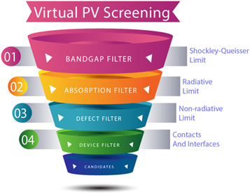
More sophisticated simulation procedures can take into account detailed balance analysis, with consideration of factors including carrier mobility and lifetimes (see figure 2) [71]. Indeed minority carrier lifetime is often the bottleneck for emerging technologies, which manifests as large open-circuit voltage deficits. For this reason, the majority of materials modeling of photovoltaic materials is focused on identifying defects that can give rise to non-radiative recombination [72]. While in the past, only the position of the defect levels in the band gap were accessible, recent progress has made prediction of carrier capture and recombination rates possible from first-principles [73]. In this way the most detrimental defects can be identified, for example SnZn and VS are predicted to act as giant carrier traps in Cu2ZnSnS4 [74]. However, such calculations are challenging in terms of human effort and calculation time so they have been performed for very few systems.
Figure 2. The hierarchy of screening potential solar absorber materials based on materials modeling. Step 1 involves the simplest metric, the Shockley–Queisser limit, that is determined by the band gap alone. More sophisticated filters involve consideration of the frequency-dependant absorption and reflectivity (Step 2) and equilibrium populations of point defects (Step 3). Steps 1–3 are based on properties that can be calculated from first-principles using modern electronic structure theory. Finally in Step 4, by considering interfacial and transport processes, a full device model can be constructed to predict J–V curves and photovoltaic performance. Materials that survive such a multi-step screening procedure, and are predicted to be thermodynamically and dynamically stable, would be viable candidates for new photovoltaic technologies. This screening hierarchy is inspired by [71].
Download figure:
Standard image High-resolution image
Progress in this field is rapid with ongoing explorations of metal oxide, chalcogenide, pnictide and halide semiconductors, as well as their mixtures. Materials modeling is already established as an essential tool in the characterization and optimization of photovoltaic materials and processes; however, with further development it has the potential to deliver greater impact by directing researchers to the promising classes of materials that have yet to emerge.
Acknowledgments
ES thanks H2020 EU Programme under the projects STARCELL (H2020-NMBP-03-2016-720907) and INFINITE-CELL (H2020-MSCA-RISE-2017-777968), the Spanish Ministry of Science, Innovation and Universities for the IGNITE project (ENE2017-87671-C3-1-R), and the European Regional Development Funds (ERDF, FEDER Programa Competitivitat de Catalunya 2007–2013). IREC belong to the SEMS (Solar Energy Materials and Systems) Consolidated Research Group of the 'Generalitat de Catalunya' (Ref 2017 SGR 862). AW is supported by a Royal Society University Research Fellowship. JDM is supported by an EPSRC Early Career Fellowship (EP/N014057/1). LHW thanks Shreyash Hadke for compiling the selected literature for complex chalcogenides and acknowledges funding from CREATE Programme under the Campus for Research Excellence and Technological Enterprise (CREATE), which is supported by the National Research Foundation, Prime Minister's Office, Singapore; and Ministry of Education (MOE) Tier 2 Project (MOE2016-T2-1-030). AZ was supported by the US Department of Energy (DOE) under Contract No. DEAC36-08GO28308 with the Alliance for Sustainable Energy, LLC, the manager and operator of the National Renewable Energy Laboratory (NREL), with the funding provided by the Office of Energy Efficiency and Renewable Energy (EERE), Solar Energy Technologies Program (SETP). AZ would like to thank Dean Levi at NREL for useful discussions. XH thanks Australian Renewable Energy Agency (ARENA) for the projects 1-USO028 and RND004 and Australian Research Council (ARC) for the project LP150100911.
Disclaimer
The information presented in this review was selected in good faith by all the authors. Errors and omissions will be corrected in the subsequent editions of the Table. Corrections and more complete information from the scientific community are most welcome in order to improve the accuracy of the values presented in the Efficiency Tables.
Authors description and contribution
Professor Lydia H Wong, contributed to compile the information about complex chalcogenides (4 atoms or more), and to write section 3.2. Dr Andriy Zakutayev: contributed to compile the information about oxides and pnictides, and to write sections 1.4, 3.1 and 3.3. Dr Jonathan D Major, contributed to compile the information about simple chalcogenides (3 atoms or less), and to write section 3.2. Associate Professor Xiaojing Hao, contributed to compile the information about complex chalcogenides (3 atoms or more), and to write section 3.2. Professor Aron Walsh, contributed to write section 4. Dr Teodor K Todorov, contributed to compile the information about simple chalcogenides (3 atoms or less), and to write section 3.2. Dr Edgardo Saucedo, acted as leader and corresponding author of the paper. He contributed to compile the information about halides and build the complete version of the Efficiency Tables, and to write sections 1.1–1.3, and 3.4.
All the authors contributed equally to define the structure and content of the manuscript, to the general review and final approval of the paper.