

Abstract
Diluted magnetic semiconductor (DMS) nanostructures are promising platform to modulate carriers and spins for new information devices. Here we report that the high quality pure CH3NH3PbBr3 microrods and Mn doped CH3NH3PbBr3 microrods have been prepared by solution method and in which the exciton magnetic polarons (EMP) formed in Mn doped microrods, and a single mode lasing phenomenon from collective EMP in single microrod have been detected when excited by fs pulse laser. This finding helps to understand the exciton and spin interactions and pave ways to the realization of new type of bosonic laser.
Export citation and abstract BibTeX RIS

Original content from this work may be used under the terms of the Creative Commons Attribution 3.0 licence. Any further distribution of this work must maintain attribution to the author(s) and the title of the work, journal citation and DOI.
Introduction
Organometal halide perovskites, as a novel type of semiconductor, have attracted much attention in the world, they have high optical absorption coefficient, suitable optical band gap, longer carrier scattering distance, which could be used as a high quality photoelectric functional material including solar cell [1], photodetector [2], display [3] and lasing [4]. For example, Xing et al succeeded in growing organic–inorganic halide perovskites which have shown tunable lasing behavior [4]. Zhu et al have demonstrated the lead halide perovskites single-crystal nanowires and its broad stoichiometry-dependent tunable lasing emission [5]. Lasing from films [6] or platelets [7] of hybrid organic–inorganic perovskites has also been reported.
In previous publications on semiconductor material [4, 6–8], most of lasing behaviors come from the photoinduced electron–hole recombination, few of them come from the exciton–exciton scattering directly in nanostructure [9] or exciton–photon coupling cavity. Due to the carrier effect, the laser emissions in the electron–hole recombination system usually have broad band and bad coherence, which have limited their further applications in the quantum information technology. So the cavity exciton–photon technique to confine high density excitons by photon has been developed [10]. In a recent publication [11], we proposed a new way to bind multi-excitons by ferromagnetic coupled spins in CdS:Co Diluted magnetic semiconductor (DMS) nanostructure, which can lead to collective exciton magnetic polarons (EMP) to give single mode lasing at pulse laser excitation. In contrast to the scattering lasing by exciton in traditional semiconductor; EMP existence in micrometer structure can enhance the coupling between exciton and EMP within a domain as represented by a new bosonic laser mechanism. Such spin-polarized coherent radiation has important applications in the spin-modulated information technology. So, it is important and challenging to find existence of spin modulation in ferromagnetic semiconductor materials which is applicable in various application.
Here we have synthesized high quality pure CH3NH3PbBr3 microrods and Mn doped CH3NH3PbBr3 microrods by solution method. The temperature related photoluminescence (PL) and stimulated emission of Mn2+ doped microrod have been studied, which prove a clear coupling between exciton and spins by EMP formation and lasing, this laser behavior will find applications in many new information technologies.
Experimental methods
Synthesis of CH3NH3Br
CH3NH3Br were synthesized by reaction of the methylamine and HBr solution. Firstly, methylamine in absolute ethanol (60 ml, 40%) was stirred for 2 h and cooled to 0 °C with the addition of HBr (65 ml, 48%). Then the solution was kept in container without stirring for 1 h. Then rotary evaporation was applied to evaporate the solvent at 50 °C. The precipitate was washed three times with diethyl ether and dried under vacuum (60 °C, 24 h).
Synthesis of CH3NH3PbBr3 microrods
CH3NH3PbBr3 microrods were synthesized by the reaction of Pb(Ac)2 and CH3NH3Br. Firstly, Pb(Ac)2 film was prepared by spin-coating on glass substrate which was cleaned ultrasonically. Then the Pb(Ac)2 glass substrate was immersed in CH3NH3Br solution in isopropanol (1 ml, 5 mg ml−1) for 15 h. The substrate was dried naturally after cleaned several times by methylamine in absolute ethanol. Finally, CH3NH3PbBr3 microrods formed on the glass substrate.
Synthesis of Mn2+ doped CH3NH3PbBr3 microrods
Mn2+ doped CH3NH3PbBr3 microrods were synthesized by the same method. A proper amount of manganese acetate was added into the Pb(Ac)2 solution before preparing the Pb(Ac)2 film. Then the homogeneous solution containing Pb2+ and Mn2+ precursor was dropped on the glass substrate. After spin coating, the glass substrate covered with Mn2+ doped Pb(Ac)2 film was transferred to hot stage with 75 °C for 30 min. Then the glass substrate coated with Mn2+ doped Pb(Ac)2 film was carefully immersed in CH3NH3Br solution in isopropanol more than 15 h. Finally the Mn(II) doped CH3NH3PbBr3 microrods were obtained.
Characterization
The morphology and composition of the samples were characterized via scanning electron microscopy (SEM, Zeiss Supra55) equipped with EDS. The phase purity of the product was examined via XRD by using an x-ray diffractometer (Brucker D8-advance) with Cu Kα radiation (1.5406 Å), therein maintaining the operating voltage and current at 40 kV and 40 mA, respectively. During the measurement 2θ ranged from 20° to 80° with a step of 0.02° and a count time of 1 s is used.
The PL, polarized PL spectra of a single microrod were measured by the same laser confocal optical microscopy (Horiba JY iHR550, Olympus BX51 M) using 405 nm continuous wave (CW) semiconductor laser as excitation source. The low-temperature PL spectra of single microrod, placed in a microscope cryostat, have been obtained on the same confocal optical microscopy. Liquid nitrogen was used to cool the samples down to 77 K. The lasing spectra of a single microrod are obtained by using a femtosecond laser (400 nm, Coherent, 130 fs, 80 MHz) for excitation.
The magnetization (M) of the product as a function of H is obtained by using vibrating magnetometer, its magnetic hysteresis behavior is observed at room temperature, as shown in figure 2(a). The M–T relationship is obtained by using a superconducting quantum interface device (SQUID, MPMS-XL-7, Quantum Design) magnetometer in the range −7 ≤ H ≤ 7 T. The temperature is changed from 2 to 300 K. All magnetization measurements were performed in the presence of an in-plane magnetic field on the massive sample on a pure silicon wafer. The measured magnetization data were corrected by subtracting the diamagnetic contribution from the Si substrate.
Results
The SEM morphology images of as-prepared microrods and Mn doped microrods are shown in figures 1(a) and (b) respectively. The two images show that the surfaces of microrods are clean and smooth. The length of as-grown microrods is about 50–100 μm. The element composition of the microrods in figure 1(a) was C, N, Br and Pb according to the energy dispersive x-ray (EDX) analysis (figure 1(c)). The element ratio of Br to Pb is 2.9, quite close to stoichiometry ratio of 3. Figure 1(d) shows the EDS profile of CH3NH3PbBr3:Mn microrods, in which the Mn concentration is about 0.21%. In the growth process the manganese concentration tuned from 0.21% to 7.35% (atomic%) can be identified by EDX. XRD patterns of pure and Mn doped microrods confirms their crystal phase and lattice quality (figure S1 is available online at stacks.iop.org/JPCO/1/055018/mmedia).

Figure 1. (a) SEM image of as-grown CH3NH3PbBr3 microrods. (b) SEM image of as-grown Mn2+ doped CH3NH3PbBr3 microrods. (c) EDX profile measured from one microrod. (d) EDX profile of Mn2+ doped CH3NH3PbBr3. Inset is the relevant element ratio.
Download figure:
Standard image High-resolution imageFigure 2(a) shows their magnetization hysteresis loop line of CH3NH3PbBr3:Mn at 0.67% Mn doping as a function of the applied magnetic field (H). The inset is the magnified area near zero magnetic fields. A good magnetic hysteresis loops was shown in M–H curves (−1000 ∼ 1000 Oe), indicating the combining ferromagnetic and paramagnetic behavior of these single-crystal. To determine its Curie temperature, we also measured the M–T curve by applying a 7 Tesla magnetic field by SQUID, as shown in figure 2(b). The magnetization slowly decreases with increasing temperature, cross point at Curie temperature has not been seen even up to room temperature.
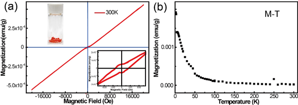
Figure 2. (a) Hysteresis loops (M versus H) of doped CH3NH3PbBr3 single-crystal measured at 300 K. Inset is the CH3NH3PbBr3 single-crystal in the vial. (b) The relationship between Magnetization and Temperature of CH3NH3PbBr3 single-crystal.
Download figure:
Standard image High-resolution imageFigures 3(a) and (b) shows respective room-temperature PL spectra of pure single CH3NH3PbBr3 microrod and Mn-doped CH3NH3PbBr3 microrod excited by 405 nm CW semiconductor laser, its PL image is shown in figure S2. A very strong band-edge emission band centered at 539 nm was observed for CH3NH3PbBr3 microrod (figure 3(a)), while two emission peaks at 543 and 557 nm showed up for Mn-doped CH3NH3PbBr3 microrod. These PL spectral profiles are different from nanodots and nanoplates emission [12], especially they were doped with Mn(II) [13]. The difference of emission peak lies in two reasons: (1) the band-edge emission peak shows red shift from 539 to 543 nm because of manganese doping, the former energy should occur at band-edge containing absolute components due to the exciton–phonon coupling in a normal polar semiconductor. But in Mn-doped CH3NH3PbBr3 microrod, the 543 nm peak should be the free exciton of CH3NH3PbBr3 microrod, its enhanced exciton–phonon coupling component should show up in the longer wavelength range than 539 nm [14]. The shift of band-edge emission also depends on the Mn2+ doping concentration of doped microrods, which can be seen in figure S5. (2) The second emission peak at 557 nm for CH3NH3PbBr3:Mn can be assigned to EMP emission [15], which is formed due to coupling between ferromagnetic coupled transition metal ion aggregate [16] and photo-induced exciton (FX) [15]. Farther from band-edge than FX, EMP contain some component FX coupling with LO phonon and collective spins, which is more stable than FX. The temperature dependent PL spectra for Mn doped CH3NH3PbBr3 single microrod have been shown in figure S4, their band-edge shift with temperature according to the Varshni function, which is identified to be in relation to the clear electron-LO-phonon coupling. The FX and EMP have a same tendency for their couplings with LO phonons, which is in contrast to the no shift of the emission energy of the bound magnetic polaron with temperatures in different DMS [11, 17, 29].

Figure 3. (a) PL emissions from a single pure CH3NH3PbBr3 microrod and (b) Mn-doped CH3NH3PbBr3 microrod at room temperature. (c) The polarized spectra of Mn-doped CH3NH3PbBr3 microrod, inset is optical image of the microrod. (d) PL intensity ratios I2/I1 of the Mn-doped microrod as a function of polarized angles.
Download figure:
Standard image High-resolution imageBecause EMPs contain polarized spin out of multi-Mn ions, their emissions have narrow polarized nature, which is not in agreement with the rod axis direction as shown in figures 3(c) and (d), as that of the Co-doped CdS belt [11]. figure 3(c) shows the polarized PL spectra of Mn-doped CH3NH3PbBr3 microrods. The detection angle was changed stepwise from 0° to 30° through a rotating optical polarizer. As shown in figure 3(d), the Mn doped microrod has linearly polarization emission, which show different polarization profile as compared with those axis-related FX luminescence as in figure S6. This difference indicates that the spin polarization has no direct dependence on the rod axis, while the PL polarization profile of pure CH3NH3PbBr3 nano-platelet is related to its crystal orientation [12] as the FX in this rod.
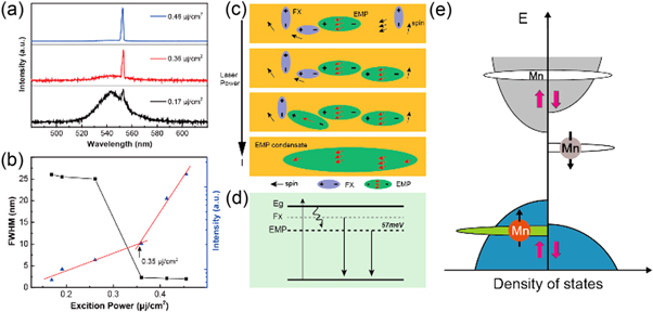
Figure 4(a) shows the PL spectra of CH3NH3PbBr3 with 0.21% Mn(II) doping concentration excited by a fs laser (400 nm), whose optical image at low excitation power is shown in figure S3. PL spectra from spontaneous emission to stimulated emission at 552 nm can be seen clearly. The PL emission intensity and FWHM is extracted and plotted as a function of excitation fluence (figure 4(b)). When the excitation fluence below 0.35 μJ cm−2, broad spontaneous emission band could be observed in PL spectra. However, the emission intensity increases superlinearly when the excitation fluence over 0.35 μJ cm−2. Moreover, their FWHMs become narrower (even to 1.45 nm width) with higher excitation fluence. The most important phenomenon here deserve to be emphasized is the single mode lasing at around the EMP energy, which is much different from that the multi-mode lasing reported early due to the cavity effect in one nanowire [5]. The multi-mode lasing of pure perovskite micro-rod spectra has been shown in figure S7. The EMP energy level of CH3NH3PbBr3:Mn microrod is separated from FX as shown in figure 4(d).
Figure 4. (a) The simulated emission of CH3NH3PbBr3 microrods with 0.21% Mn(II) doping concentrations. (b) The PL emission intensity and FWHM is extracted and plotted as a function of pumping power. (c) The schematic of EMPs formation in perovskite. (d) The luminescence schematic of FX and EMP. (e) Band-structure of Mn doped Perovskite semiconductor.
Download figure:
Standard image High-resolution image
Discussion
The ferromagnetic mechanism of DMS usually comes from the spin-spin coupling and spin-carrier interactions. The former often dominate in the doped wide-gap semiconductor with a high Curie temperature, in which some of the d level is located within the bandgap, while the latter has a determining contribution in the narrow gap semiconductor simultaneously with a low Curie temperature, in which the d levels are buried within the valence band and conduction band, as shown in the figure 4(e) [19]. From such band-structure diagram, we can found that the band-edge can be modified with the spin-spin couplings between carriers. If the ferromagnetic coupling dominates the band-edge of a DMS, it red-shifts, while it blue-shifts if the antiferromagnetic coupling dominates the band-edge. This microscopic interaction character has been identified by our experimental results in Mn [16] or Co doped CdS nanostructures [11], and Mn doped ZnO nanowire [18]. The CH3NH3PbBr3 belongs to the wide-gap semiconductor (>2 eV), so its magnetization as measured in figure 2(a) is mainly come from Mn–Mn ferromagnetic coupling or (MnBr)n cluster as that shown in CdS:Mn belt although there are lots of independent Mn(II) inside the CdS lattice [16]. This type of Mn–Mn ferromagnetic coupling can leads to the formation of EMP at the lower energy side of band-edge if excitonic effect is dominant. If the excess carrier effect is substantial in this doped DMS, the optical and transport behaviors will be different [19, 20]. Li et al have proposed another potential application of photoinduced spin current effect in organic–inorganic lead halide perovskite [21], may influence its photovoltaic effect due to the spin–orbit coupling. Clearly this effect need special light to orientate carriers and/or spins. Though this phenomenon is not related to ours, for we excite magnetic excitons with spontaneous ferromagnetism in semiconductor microstructures, the spin–orbital coupling may relax EMP state to carriers [14]. Here our micro-luminescence results indicate the EMP near band-edge and their lasing profile is a clear verification of photoinduced collective EMP transition before exciton dissociation, indicating a strong spin-polarized exciton (coherent EMP) behavior but not carrier effect in this diluted Mn doped CH3NH3PbBr3 as described in next section. This result indicated that the ferromagnetic spin coupling between Mn ions but not spin–orbit coupling dominated their band-edge excitonic nature at high excitations.
After photoexcitation above bandgap, the produced free exction could couple with ferromagnetic coupled cluster directly to form EMP, both of them can exist in nanostructure [16]. Such EMP shows up at a lower energy, hence has a much larger binding energy than FX. From separation of FX and EMP emission peaks in figure 3(b), the binding energy difference for EMP to FX could be calculated to reach to 57 meV, much stable at room temperature (kT = 26 meV). It is well known that FXs in CH3NH3PbBr3 can dissociate into electrons and holes easily to contribute to conduction, hence to be used for solar cell [1, 22]. The stability of excitons is strongly dependent on their composition, size and microstructure [23]. In contrasting to the reported free excitons, EMPs as formed near the ferromagnetic cluster does not dissociate into electron and hole at room temperature, but couple with each other via exchange interactions if more EMPs are excited. EMP is often found to be the coupling composite of FX, coupled spins and LO phonon in polar semiconductors, all with a bosonic nature [11]. This bosonic composite excitation in DMS nanostructure can produce collective EMP within a critical domain [25], like a nonequilibrium bosonic condensate, to emit light coherently [14]. This type of lasing looks like exciton-polariton laser, the exciton–photon coupling excitation, in a semiconductor microcavity [10], in which the photon by an outer laser is used to confine multi-excitons within a microcavity, then produce bosonic lasing. This is different from F-P mode laser which depends on the micro-structure and morphology of a nanowire [24]. However, the collective EMP lasing do not need a cavity [25], whose confining force comes from the intrinsic ferromagnetic coupling spin cluster inside the DMS nanostructure, whose confining space depends on the ferromagnetic coupled Mn(II) cluster and nearby single Mn ions. High density excitons excited by fs laser will drop into the EMP states to behave with consistently coupled spins. Their coherent radiation happens with the photo-induced spin-polarization character, as described in figure 4(c).
All above optical experimental results were obtained at room temperature. A ferromagnetic spin cluster formation in a DMS nanostructure should be a crucial condition [15, 16] to bind the exciton and spins, and to produce EMP, hence leading to its individual EMP luminescence band, finally produce single mode bosonic lasing during high concentration of EMPs are excited. The CH3NH3PbBr3:Mn QDs have also been synthesized and produce tunable size-dependent band-edge emission, together with a Mn ion d–d transition emission band [13, 26]. This emission behavior of QD show no emission profile from the ferromagnetic-coupled Mn ions, i.e. EMP peak at room temperature as shown in the microrod above. That means the EMP formation need large size to induce multi-Mn ions ferromagnetic coupling and related LO phonon polarization. QD with quantum confinement could not afford the ferromagnetism of Mn ions to exist in nanometer size, but micrometer sized rod can do. Without the formation of EMP, the exciton in QD can easily relax into the in-gap trapped d state of doped Mn ions, which lead to the d–d transition emission. This character also reflected the high stability of EMP, which can bind to FX and reduce inner radiationless relaxation, possibly to form multi-EMP. So the collective EMP lasing effect in micrometer size as above can happen in a critical size much larger than several nanometers, which is an interesting size effect for exciton and EMP in DMS, deserving further study. We also find similar behavior in ZnSe:Mn QDs [27] and nanowires [28], the d–d transition emission can be more easily found in its QDs but not nanowire or belt. Due to the polarization nature of EMP, this DMS nanostructure is clearly a typical platform for the study on the spin-polarized exciton system.
Conclusion
In summary, high quality CH3NH3PbBr3, CH3NH3PbBr3:Mn microrods and their single-crystals have been synthesized. The Mn(II) doped CH3NH3PbBr3 behaves with DMS nature. The PL emission and magnetic behavior of microrods in a range of Mn doping concentration indicate a new excitation formation—EMP with higher stability than FX. This EMP comes from the interactions between exciton and ferromagnetic coupled TM ions. High density EMP can form collective EMP to produce single mode lasing emission with specific polarization profile, which is proved not depend on the formation of optical cavity. Therefore the Mn doped CH3NH3PbBr3 perovskites can be used to study the exciton condensate behavior and find applications in the spin-polarized photonics devices and quantum information processing in future.
Acknowledgments
The authors thank the 973 project (2014CB920903) of MOST and the Special Key Project for the National Strong Magnetic Field Center at Huazhong University of Science and Technology (HUST) (No. 2015KF03) for financial support. The authors declare no conflict of interest.