
Abstract
Within the last decade, novel materials concepts and nanotechnology have resulted in a great increase of the conversion efficiency of thermoelectric materials. Despite this, a mass market for thermoelectric heat-to-electricity conversion is yet to be opened up. One reason for this is that the transfer of the lab records into fabrication techniques which enable thermoelectric generator modules is very challenging. By closing the gap between record lab values and modules, broad industrial applications may become feasible.
In this review, we compare three classes of materials, all designed for medium-high to high temperature applications in the field of waste heat recovery: skutterudites, half-Heusler compounds, and silicon-based materials. Common to all three classes of thermoelectric materials is that they are built from elements which are neither scarce (e.g. tellurium) nor toxic (e.g. lead) and therefore may be the foundation of a sustainable technology. Further, these materials can provide both, n-type and p-type materials with similar performance and thermomechanical properties, such that the fabrication of thermoelectric generator modules has already been successfully demonstrated. The fabrication processes of the presented materials are scalable or have already been scaled up.
The availability of thermoelectric materials is only one important aspect for the development of thermoelectric generator modules and heat conversion systems based on this technology. The design and configuration of the thermoelectric generator modules is similarly important. Hence, basic considerations of module configuration and different fundamental layouts of the thermoelectric heat-to-electricity conversion system are discussed within an additional chapter of this review.
Export citation and abstract BibTeX RIS

Content from this work may be used under the terms of the Creative Commons Attribution 3.0 licence. Any further distribution of this work must maintain attribution to the author(s) and the title of the work, journal citation and DOI.
1. Introduction
Waste heat is necessarily produced by all processes that do work, e.g. by combustion engines that release heat to the environment. Sources of waste heat include vehicles, power stations, industrial plants like oil refineries and steelmaking plants. If it were possible to recycle just a small proportion of this energy into a superior grade of energy, which can either be better stored or better transported than waste heat, a considerable contribution to the reduction of the world's fossil fuel consumption and carbon dioxide production would be the consequence. One technology discussed for the recovery of waste heat from high temperature processes is thermoelectricity.
Thermoelectric generators (TEGs) convert heat flows directly into useable electrical energy and vice versa. In an appealing scenario of application, waste heat, e.g. from the exhaust gas pipe of a vehicle, could be partly recovered by thermoelectric generators. It is typically argued that the heat comes with no additional costs. Hence, every contribution of a thermoelectric generator would result in an increase of the over-all process efficiency—even a small one. In that sense, thermoelectricity could play a role in the energy mixture of our future. Yet, making high-efficiency thermoelectric materials and modules available for the application scenario of waste heat recovery is an enormous challenge for research and development. This article will therefore review some promising materials for the medium-high to high temperature thermoelectric heat-to-electricity conversion as well as important considerations for the device design.
The thermoelectric generator is placed between a heat source at temperature Thot and a heat sink at temperature Tcold. At an average temperature T, the conversion efficiency of a thermoelectric material is defined by the dimensionless thermoelectric material's figure of merit zT

where α, σ, and κ are the Seebeck coefficient, electrical conductivity and thermal conductivity, respectively, and α2σ is called the power factor. Good thermoelectric materials have a high Seebeck coefficient, α, expressing the generated thermovoltage per temperature difference and hence defining the output voltage of the generator. A high electrical conductivity, σ, is necessary for a small internal resistance of the generator. Thermal conduction through the device works continuously against the external temperature difference and is one major loss mechanism of the thermoelectric generator. Consequently the thermal conductivity, κ, has to be low. This combination of properties is rare. For decades, the best materials' figures of merit were measured at around zT  1, and it is often argued that zT
  1.5 is necessary for most technical applications [1]. On the other hand, the intrinsic efficiency of the material is only one issue for a technical application—the availability and costs of the thermoelectric material, the total costs of the system or the long term stability of an installation are concerns which may be even more important.
Material challenges
In a review by Snyder and Toberer from 2008 [2], figure of merit data of state-of-the-art commercial materials and those used or being developed by NASA for thermoelectric power generation are compared for the different temperature regimes. The materials listed there are: Bi2Te3, Sb2Te3, PbTe, CoSb3, CeFe4Sb12, Yb14MnSb11, (GeTe)0.85(AgSbTe2)0.15 (commonly referred to as TAGS) and SiGe. In particular, tellurium (Te) is a relatively scarce and hence expensive element, preventing the use of thermoelectric generators based on this element for large scale applications.
The vision of an application in waste heat recovery has motivated researchers all over the world to accept the challenge of designing novel high zT materials, partly as substitute materials for conventional thermoelectric materials which are not considered sustainable. An improved understanding of the interrelation of the involved transport coefficients has increased zT dramatically over the last decade, and nanotechnology is one important driving force of this development. The idea that single nanoscopic objects have a higher figure of merit than the bulk counterpart by quantum confinement of electrons and phonons, e.g. in nanowires or quantum well structures [3–6], has since pushed the thermoelectric community towards the design of thermoelectric materials on all length scales, from nanoscopic up to mesoscopic and macroscopic architectural elements. Famous examples are quantum well structures [6] and quantum dot superlattice structures with impressive zT values [7, 8]. These low-dimensional structures combine an increase of the power factor with a reduction of the lattice thermal conductivity due to a modified electronic density of states and a freezing of phonon modes. Single nanowires [9, 10] and porous nanomeshes [11] can also be used to boost the figure of merit compared to the bulk counterparts of the material.
Isolated nanowires are difficult to integrate into macroscopic waste heat recovery systems. A more pragmatic way of optimizing the thermoelectric performance is the introduction of nanostructural elements into bulk materials. The fundamental idea of this approach is that electrons and phonons have quite a different mean free path in many materials: the mean free path of phonons in most covalently bonded materials is considerably longer than the typical length scale imposed into the material by the nanostructure, i.e. mean crystallite size. The mean free path of the electrons in thermoelectrically optimized material is, on the other hand, determined by scattering at impurity atoms like the charged cores of the substitutional dopant atoms and thus much smaller than the mean crystallite size. An optimization of the thermoelectric material can therefore be done by a reduction of the grain size of the thermoelectric material down to the length scale of 10–100 nm [12–15], and several reviews address advances in this field [16–20]. Similarly, the implementation of nanoscopic precipitates targets a reduction of the thermal conductivity [21]. Recently it was pointed out that only by addressing both the nano- and microstructure with a hierarchical design of the material on all length scales do record zT values >2 become possible [22]. Within this approach of tuning the nano- and microstructure of a material for increased zT values, the availability of high quality nanopowder fostered the development of novel thermoelectric materials: materials which have per se an insufficient thermoelectric figure of merit can be optimized such that they may become interesting alternatives as sustainable substitute materials like nanocrystalline silicon [23, 24].
Another important trend in the development of novel thermoelectric materials is the use of materials with relatively complex elementary cells and rich alloying of those materials. Materials with complex elementary cells generally favor a low thermal conductivity due to many flat optical modes in the phonon dispersion relation which do not contribute much to the heat transport due to a low group velocity. The implementation of rattling atoms at weakly bound lattice sites further reduces the lattice thermal conductivity by creating additional scattering processes for the phonon transport. Rich alloying with many different elements, on the other hand, creates point defects which intrinsically deteriorate the thermal conductivity but sometimes may also compromise the mobility of carriers. Richly alloyed skutterudites and half-Heusler compounds with a complex nano- and microstructure are promising materials for medium-high to high temperature thermoelectric heat-to-electricity conversion which combine these different concepts.
Device challenges
The efficiency of a thermoelectric generator module is not only a function of the material's figure of merit zT, but to a large degree a function of the thermoelectric generator module (TGM) itself. A conventional TGM is sketched in figure 1. A thermoelectric couple consists of a p-type semiconductor and an n-type semiconductor. Both are electrically connected in series and thermally connected in parallel. The maximum conversion efficiency of the thermoelectric process in near equilibrium conditions is (e.g. [25]):
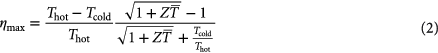

Figure 1. Schematic of a conventional thermoelectric generator showing the parallel thermal connection and series electrical connection of the semiconductor legs as well as the cold side and hot side substrates.
Download figure:
Standard image High-resolution imageHere ZT is the figure of merit of the TGM, which is distinguished from the material's figure of merit zT by a capital Z. ZT includes electrical and thermal losses at the non-ideal contacts of the device.
Typically, applications are distinguished according to the target temperature of the hot side and cold side since different materials and different fabrication technologies are needed for each temperature range. LeBlanc [26] classifies four different temperature scenarios: low temperature (Thot = 100 °C, Tcold = 20 °C), medium-low temperature (Thot = 250 °C, Tcold = 20 °C), medium-high temperature (Thot = 500 °C, Tcold = 50 °C), and high temperature (Thot = 800 °C, Tcold = 50 °C).
Commercially available TGMs typically work in the low temperature regime and are based on telluride materials. A comparison of 21 commercial TGMs from different manufacturers is given in a recent review [27]. Full characterization of conventional thermoelectric generator devices produced from novel materials for the medium-high to high temperature regime is still rare in the literature. Bartholomé [28] and coworkers produced a TGM based on half-Heusler compounds (Zr0.4Hf0.6NiSn0.98Sb0.02) which had a device ZT = 0.44 operated with Thot = 530 °C and Tcold = 30 °C. Kessler and coworkers fabricated TGMs based on nanocrystalline silicon [29]. A device ZT = 0.13 was achieved at 600 °C. TGMs based on oxide thermoelectric materials were recently reviewed in [30]. For instance, a module based on p-Ca3Co4O0.9 and n-Zn0.98Al0.02O was operated at Thot = 630 °C and Tcold = 140 °C, and a thermoelectric unicouple consisting of p-Ca2.7Bi0.3Co4O9 and n-La0.9Bi0.1NiO3 could be operated at Thot = 800 °C and Tcold = 223 °C [31]. Although skutterudite powders (zT ~ 1 after hot pressing for both n- and p-type) are available from large scale production (>500 kg a−1 fromTreibacher Industrie AG), devices are only produced in small scale operations. Guo et al [32] fabricated a skutterudite module with size of 50 mm × 50 mm × 7.6 mm with 8% thermoelectric conversion efficiency and a power output of 32 W working in a temperature gradient from Thot = 600 °C and Tcold = 50 °C. A conversion efficiency of 7% was demonstrated at ΔT = 460 °C for a 32 couple skutterudite module by Salvador et al [33]. A recent comparison [34] of several lab-built devices (based on PbTe, Mg2(Si,Sn), skutterudites and half-Heusler compounds, revealed a power density of 0.75 W cm−2 and the highest TE-efficiency of 8% for the skutterudite module (based on commercial powder; zT ~ 1 after hot pressing for both n- and p-type) in a temperature gradient Thot = 550 °C and Tcold ~ 27 °C.
While commercial TGMs are available for low and medium-low temperatures, medium-high to high temperature TGMs are only very rarely commercially accessible. Thermoelectric generation in this temperature regime is used only for very limited applications in spacecraft, where thermoelectric generators provide electricity for deep space missions, which are too far away from the sun to use photovoltaic cells. For instance, thermocouples made from heavily doped n-type and p-type silicon–germanium alloys were used in nuclear powered thermoelectric generators providing onboard power to the American voyager spacecraft [35]. Such radioisotope thermoelectric generators have been working for decades now. Unlike on Earth, neither oxidation nor thermal cycling is an issue in the case of extraterrestrial use.
TGMs are themselves only an intermediate product, since the application requires an integration of the TGM on the system level. The great challenge of opening new markets for thermoelectricity in the recovery of waste heat thus creates a need, not only for high efficiency thermoelectric materials, but also for generator modules and the complete heat conversion system to be developed, and the gap between modules and applications also has to be bridged. In principle, all modules need to be designed exclusively for the required application, and some fundamental considerations for the module design, for instance with respect to the thermal conductivity, will be addressed in section 3.
Medium-high to high temperature waste heat recovery is the most appealing scenario from the viewpoint of thermodynamics. The operating temperatures together with the figure of merit define the efficiency of the thermoelectric conversion by the Carnot limit, and high temperature applications with large ΔT are generally favored. Figure 2 displays the maximum efficiency from equation (2) for the different materials discussed in this review; half-Heusler compounds, skutterudites and low zT materias (i.e. silicon). In this perspective the cold side is kept constant at room temperature and the hot side is based on a conservative estimation from the material properties.

Figure 2. Plot of the maximum efficiency from equation (2) with Tc = 300 K shows the importance of zT and ΔT.
Download figure:
Standard image High-resolution imageApplications which offer hot side temperatures in the medium-high to high temperature regime are manifold, and the big players are automotive application and industrial waste heat recovery like in heavy industry—cooling down of steel bars, aluminum bars, steel mills, etc. In particular, the latter application requires module solutions which can be powered by radiation heat.
Only very limited work has been dedicated to the estimation of system costs for TGMs used in the different temperature regimes. Table 1, extracted from LeBlanc et al [26], summarizes estimated materials' prices (based on raw material prices of 2013), as well as estimated system costs including system components and manufacturing costs in dollars per Watt for medium-high to high temperature application. For this estimate, it was assumed that the costs of the primary heat could be neglected.
Table 1. Comparison between the three different classes of high-temperature thermoelectric materials according to [26].
| Material type | Chemical formula | Manufacturing type | Estimated material costs ($ kg−1) (2013) | Estimated module ZTm | Estimated system costs ($ W−1 m−2) medium-high T scenario | Estimated system costs ($ W−1 m−2) high T scenario |
|---|---|---|---|---|---|---|
| Skutterudites | CeFe4Sb12 | Bulk | 37 | 0.77 | 7 | 3 |
| Yb0.2In0.2Co4Sb12 | Bulk | 24 | 0.93 | 5 | 3 | |
| Ca0.18Co3.97Ni0.03Sb12.4 | Bulk | 13 | 0.77 | 7 | 3 | |
| Half-Heusler compounds | Zr0.25Hf0.25Ti0.5NiSn0.994Sb0.0006 | Bulk | 9.7 | 1.38 | 4 | 2 |
| Zr0.5Hf0.5Ni0.8Pd0.2Sn0.99Sb0.01 | Bulk | 8.5 | 0.69 | 7 | 3 | |
| Ti0.8Hf0.2NiSn | Bulk | 11 | 0.41 | 10 | 4 | |
| Silicon-based materials | Si | Nanobulk | 3.0 | 0.21 | 22 | 7 |
| Mg2Si0.85Bi0.15 | Nanobulk | 6.7 | 0.67 | 8 | 3 | |
| Mg2Si0.6Sn0.4 | Bulk | 4.0 | 1.05 | 5 | 2 |
Note: Note that cost values are rounded to the nearest dollar. There is a large range in the system costs; a representative value was selected for generating costs presented in [26]
The thermoelectric materials extracted in table 1 are pre-selected for the purpose of this review: the cheapest thermoelectric materials available in the high temperature scenario are nanobulk variants of silicon and silicides. Currently the performance, zT, of nanobulk silicon needs further optimization, but the costs of the raw material are highly competitive. Skutterudites and half-Heusler compounds are a little more costly, but their figure of merit values are already in the desirable range around zT ~ 1 or higher. Following the line of the module and system cost estimate in [26], in the case of a waste heat recovery from industrial furnaces (high temperature scenario) the costs for electricity of a thermoelectric system for some novel classes of materials can compete with electricity costs from other sources (coal, nuclear, geothermal etc) except for natural gas, where the primary energy has to be paid. Values of 2013 are given in [26] and references therein: natural gas: $0.98 W−1, coal: $2.84 W−1, nuclear: $5.34 W−1, geothermal: $4.14 W−1, organic rankine: $4.00 W−1, and thermoelectric system costs in the high-T scenario of lowest: $2 W−1(table 1).
High temperatures of several hundred degrees celsius require special materials and device concepts. On the level of the thermoelectric converter material it is required that the material is stable, i.e. does not show any phase transitions, any degradation of the nano-/microstructure nor its chemical composition, and is resistive against corrosion. On the level of the TGM, the conventional design requires a metallization at the cold and hot side of the generator. In particular, the hot side metallization is a technological challenge since it has to be perfectly electrically conductive, mechanically hold the complete device together, and be stable up to several hundred degrees celsius against inter-diffusion and oxidation. Further, for many applications, a thermal cycling induces additional thermo-mechanical stress at the semiconductor–metal interface. Especially for the desirable high temperature applications, degradation and device failure at the hot side semiconductor–metal interface are potentially problematic. As a consequence, high temperature TEGs working with large temperature differences are hardly commercially available up to now, but novel device architectures may provide a solution for this (see section 3).
Concluding, high temperature waste heat recovery is by far the most interesting potential application of thermoelectric materials from the viewpoint of thermodynamics, but also the most challenging one with respect to thermo-mechanical stress and device degradation. Section 2 of this review will therefore focus on thermoelectric materials which work in the medium-high to high temperature regime and whose development is at the edge of commercialization. Without claiming completeness, the authors have limited this choice to skutterudites, half-Heusler compounds and silicon-based materials. Where available, thermo-mechanical data will be included into the materials' review. Section 3 is dedicated to the thermoelectric generator module. Basic considerations necessary to configure the device for the application are discussed there, as well as novel device architectures which may be better suited to the recovery of radiation heat than the conventional TGM.
2. Novel thermoelectric materials for high temperature waste heat recovery at the edge of commercialization
In the following chapter, three different classes of medium-high to high temperature thermoelectric materials, i.e. skutterudites, half-Heusler compounds and silicon-based thermoelectric materials, will be reviewed with respect to their physical and thermo-physical properties as well as recent advances in materials design. Without claiming completeness, these materials were chosen according to the actual status of their development: manufacturing processes are fully scalable or have already been scaled up to technical plants, and the materials are at the edge of commercialization.
2.1. High zT-skutterudites
Skutterudites form a quite promising class of materials with high thermoelectric efficiency in the high temperature regime. The body centered cubic crystal structure of low Laue symmetry was first described by Oftedal [36] for binary CoAs3: the unit cell reveals a three-dimensional As-metal framework (As in sites 24 g), which encloses Co-atoms at the centers of tilted As-octahedra (sites 8c) and provides ample icosahedral space (in sites 2a) for the incorporation of 'filler' atoms. Hitherto a large variety of compounds and solid solutions are derived from this structure type. The filled skutterudites—like YbFe4Sb12 (LaFe4P12-type [37]) shown in figure 3—have a structural-chemical formula EPyT4X12 where EP is usually an electropositive element species enclosed by the cage structure formed by the pnicogen atoms, X, and transition metals, T, at the octahedral centers.

Figure 3. Distribution over the periodic chart of the various atom constituents forming skutterudite compounds.
Download figure:
Standard image High-resolution imageFigure 3 gives a color code for the various elements in the periodic chart with respect to their function in the stabilization of the skutterudite lattice. CoSb3 can be considered as the parent skutterudite thermoelectric material being a diamagnetic (Co3+, 3d6) narrow band gap (~0.2 eV) semiconductor with high carrier mobility and relatively large effective electron mass reaching a zT < 0.8 [38]. The electronic structure of the host lattice can be tuned by (i) chemical substitution mainly in the T-site [39–50], and (ii) by the nature of the guest atom EP in 2a and the filling level y for this site [43, 51–81]. Skutterudites comprise a wide range of physical properties [82] ranging from (a) metallic systems exhibiting heavy Fermion superconductivity (PrOs4Sb12 [83, 84]), Kondo scattering, intermediate valence (from unstable electronic configuration of rare earth elements; Yb(Fe,Co,Ni)4Sb12 [85]), strongly correlated electrons, or hopping conductivity to (b) semiconductors with metal to insulator transitions (PrRu4P12 [86, 87]), pronounced crystal field splitting, and long range magnetic order (PrFe4Sb12 [88–90]). Depending on the electron concentration tuned by chemical substitution and filling level (in general fillers are effective n-type dopants, except for iodine which acts as an electron acceptor), filled skutterudite solutions may change from an n-type to a p-type semiconductor. Numerous experiments and density functional theory calculations point towards 'rattling' (vibrational) modes of the various filler atoms in the oversized icosahedral cages, thereby helping to scatter heat-carrying phonons for low thermal lattice conductivities. In contrast to unfilled skutterudites (see for instance [91]), low-frequency vibrational modes (Einstein oscillations) have been claimed from heat capacity measurements with energies around 6 meV (~70 K) and 18 meV (200 K), which are confirmed from inelastic neutron diffraction data [60] and are consistent with ab-initio lattice dynamics calculations [92] as well as with the large atom thermal displacement parameters derived from x-ray/neutron diffraction data. Although in an inelastic resonant scattering model acoustic phonons with frequencies comparable to those of the localized modes of independent rattling filler atoms interact strongly [93], high resolution inelastic neutron scattering and time of flight experiments [94] seem to evidence quasi-harmonic filler vibrations coherently coupled with the framework atoms. Nevertheless, multifilling seems to provide lower thermal conductivity via scattering an as broad a spectrum of phonon modes as possible by selecting fillers with respect to different mass, size, coupling to the framework and vibrational frequencies [65]. A simple guide to estimate the fraction y of filler atoms FA in FAyCo4Sb12 was derived by Shi et al [95] from the correlation between the Pauling electronegativities ε of filler atom and antimony: εSb − εFA > 0.8.
Thermoelectric properties of filled skutterudites rely not only on large Seebeck coefficients (>150 μV K−1 at 580 °C) but also on high carrier densities, which rise significantly with the filling level of proper guest atoms. Filler atoms in Co4Sb12 are known to have little effect on the conduction band edge and thus do not seem to significantly alter the transport properties [96]. Singh highlighted the importance of the degeneracy of bands near the band edge at the gamma point [97]. Because the energy bands of the electrons are rather flat, high effective masses are inherent to the charge carriers and support the high Seebeck coefficients. Skutterudites are viewed as examples of the PGEC concept (Phonon Glass–Electron Crystal) proposed by Slack [98, 99]: an open crystallographic structure, where framework atoms provide excellent electronic properties, whereas filling the voids with rattling guest species reduces the lattice thermal conductivity to levels seen in amorphous structures.
Syntheses in the laboratory are generally designed to not miss thermodynamic equilibrium and thus use excessive overtime. Difficulties arise from the rather unbalanced melting points of cobalt, rare earth metals and antimony as well as from the high vapor pressures of certain filler atom species (Sr, Ba, Yb etc). In the latter cases, powders of melted CoSb3-precusor are reacted in evacuated silica vials with the volatile filler species through a long term heat treatment after which the products are ball milled and reaction sintered in graphite dies of a hot press or spark plasma sintering (SPS) device at about 700 °C and ~60 MPa. This procedure generally results in practically single phase and >98% dense bulk specimens. Several research groups claimed rapid synthesis techniques (such as melt spinning [100–102], high pressure and high temperature processes [74, 103–107], and others [108, 109]) but so far hardly approached maximum zT-values or proved scaling up abilities. However, recently a fast and reproducible large-scale production (>50 kg) of homogeneous skutterudite powders has been reported [110], which after hot-pressing reach zT of better than 1.1 and 1.3 at 500 °C for p- and n-type materials, respectively.
Among the manifold of good skutterudite thermoelectrics presented in the literature only a few systems have become known with zT values surpassing 1.2. Figures 4(a) and (b) summarize the hitherto best p- and n-type bulk skutterudites. Besides In-filled grades, triple or multiple filled Co-based solutions currently reveal the best n-type bulk materials with Sr, Ba, Yb or other light RE as filler atom species with zT = 1.4 at 540 °C to 1.7 at 576 °C [68, 70, 79, 115, 116]. In situ precipitates of Yb2O3 from excess Yb can yield zT = 1.6 at 565 °C with an average zTav ~ 1.1 (30 °C–550 °C) [80]. For p-type bulks it proved necessary to shift the Fermi level to the low energy side of the band gap. This is generally achieved by substitution of Co by Fe. The increasing Fe-content concomitantly boosts the guest atom filling level which, dependent on the electronic state of the guest atoms, defines the proper range of substitution [50, 109, 113]. The p-type skutterudites with the hitherto highest zT ~ 1.2 and an average zTav > 0.8 (for 30 °C-550 °C) are found among DDyFe4−xCoxSb12 (x ~ 1; DD stands for didymium, a natural double filler consisting of 4.76% Pr and 95.24% Nd) [43–45]. It could be shown in several studies [112, 119–126] that a substitution of Sb-atoms with non-pnicogen atoms influences the electronic structure and due to enhanced scattering of phonons on electrons and impurities reduces the lattice thermal conductivity, leading to enhanced zT values e.g. zT = 1.3 at 500 °C for DD0.59Fe2.7Co1.3Sb11.8Sn0.2 [111].

Figure 4. (a) p-type skutterudites reaching a temperature dependent figure of merit, zT > 1.0. Data composed from [a] = [44], [b] = [111], [c] = [112], [d] = [113], [e] = [50], [f] = [109], [g] = [114]. (b) n-type skutterudites reaching a temperature dependent figure of merit, zT > 1.4. Data composed from [a] = [80], [b] = [79], [c] = [70], [d] = [68], [e] = [115], [f] = [116].
Download figure:
Standard image High-resolution imageA further increase of the thermoelectric efficiency was obtained from nanostructuring by applying severe plastic deformation processes (for instance high pressure torsion (HPT)) as a tool to further reduce the crystallite size, to increase lattice defects, dislocation density etc. and thereby to increase the scattering of the heat-carrying phonons and approaching zT = 1.9 (n-type) or zT = 1.4 (p-type) at 565 °C; see figure 5 ([117] and references therein).

Figure 5. Temperature dependent figure of merit, zT, of filled p-type (red) and n-type (blue) skutterudites before and after severe plastic deformation. Data composed from [a] = [80], [b] = [117], [c] = [118].
Download figure:
Standard image High-resolution imageA material's response to thermal and mechanical stresses generated by in-service conditions of a thermoelectric module [1, 144] demands a detailed knowledge of mechanical properties such as hardness, thermal expansion (figure 6) and elastic moduli (figure 7) (for details see [118, 127, 143] and references therein), just to name the most important ones. All of these properties are strongly dependent on temperature, composition, porosity and grain size of the material. In addition, in order to avoid stresses during repeated heating and cooling cycles, all of these parameters should be as close as possible for the p- and n-type skutterudite used for a thermoelectric module [47]. The average thermal expansion coefficient  of P-based skutterudites is rather low with
  = 5.2 × 10⁻⁶K−1 in comparison to that of Ge- and As-based skutterudites with
  = 9.3 × 10⁻⁶ K−1 and
  = 9.8 × 10⁻⁶ K−1 respectively. Note that generally n-type Sb-based skutterudites have a lower coefficient of thermal expansion
  than p-type isotypes (see figure 6), however, for Fe/Ni substituted multifilled skutterudites a p- and an n-type skutterudite with practically the same thermal expansion (
 = 11.8 × 10⁻⁶ K−1 and
  = 11.9 × 10⁻⁶ K−1 respectively), identical hardness and elastic moduli with a zT ~ 1 could be produced [47]. Fracture toughness ranges between 1.5–2.8 MPam1/2, flexural strength, dependent on temperature, between 90–160 MPa (for details see [143] and references therein). Microhardness of ball milled skutterudites at room temperature is in the range of HV0.1 = 450–530.

Figure 6. Thermal expansion coefficient, α, of Sb-based skutterudites. Data composed from a = [127], b = [128], c = [129], d = [130], e = [98], f = [47], g = [131], h = [132], i = [133], j = [134], k = [135], l = [136], m = [43], n = [137], o = [46], p = [138], q = [118], r = [112].
Download figure:
Standard image High-resolution image
Figure 7. Elastic moduli of Sb-based skutterudites at room temperature: Young's modulus, E, bulk modulus, B, and shear modulus, G. Data composed from a = [139], b = [79], c = [140], d = [141], e = [142], f = [130], g = [75], h = [138], i = [143], j = [100], k = [47], l = [118], m = [137].
Download figure:
Standard image High-resolution imageIn summary we can say that careful tuning of the band gap and positioning of the Fermi level at the electronic density of states via solid solution combined with nanostructuring (generally by ball milling, melt spinning etc.) has so far yielded attractive zT values reaching thermoelectric conversion efficiencies of about 14% (for a single leg) in the medium-high temperature range (RT to 550 °C) characteristic for automotive applications.
2.2. Thermoelectric half-Heusler compounds
The so-called Heusler compounds were discovered in 1903 by Fritz Heusler [145]. Heusler compounds conform to the elemental formula X2YZ. Certain compounds of this materials class are ferromagnetic, even though they do not contain any ferromagnetic elemental components. These materials have a high impact in spintronics [146–148]. The half-Heusler (HH) compounds are a variant of the Heusler compounds with the elemental formula XYZ. HH materials consist of three interlaced face-centered cubic sub-lattices (see Figure 8). Many of them are characterized by narrow band gaps [149, 150], suitable for thermoelectric properties [151, 152]. Nevertheless, only a few HH compounds have been studied extensively for their thermoelectric properties, suggesting that advanced materials design is an important option to explore and make progress in this area.

Figure 8. Periodic table of the elements. The huge number of HH materials can be formed by combination of the different elements according to the color scheme (left). Crystal structure of a HH compound (right).
Download figure:
Standard image High-resolution imageA great advantage of HH compounds is the possibility to dope each of the three occupied fcc sublattices individually in order to optimize the thermoelectric properties. For example, it is possible to alter the number of charge carriers by doping on the Z position, and simultaneously introduce disorder by doping on the X and Y positions, resulting in mass fluctuations, which can decrease the thermal conductivity κ. The most attractive properties of HH materials for thermoelectrics are their high Seebeck coefficient of up to ≈300 µV K−1 at room temperature and their high electrical conductivity (≈1000–10 000 Scm-1) [153–157]. The only drawback is the relatively high thermal conductivity, which can be as high as 10 Wm−1 K−1.
According to the literature, both n-type compounds with the elemental formula MNiSn (M = Ti, Zr, Hf) and p-type MCoSb display a high potential for exceptional zT values. Research has, therefore, focused mainly on improvement of these ternary intermetallic compounds. A general challenge in improving HH compounds is the comparatively high thermal conductivity of the order of 10 Wm−1 K−1. A common approach to reduce thermal conductivity is to increase phonon scattering. Hohl et al [158] reduced the thermal conductivity by a factor of three for different temperatures by introducing disorder on the X-sites of X0.5X'0.5NiSn (X, X' = Ti, Zr, Hf). Substitution of tin by antimony increases both the thermal and electrical conductivities [149]. Substitution at the Ni position also decreases the thermal conductivity [159]. The composition Zr0.5Hf0.5Ni0.8Pd0.2Sn0.99Sb0.01 possesses a figure of merit zT = 0.7 at 527 °C [160] and the composition Hf0.75Zr0.25NiSn0.975Sb0.025 shows a figure of merit zT = 0.8 at T = 800 °C [161]. Toyota (Japan) measured zT = 0.9 for Hf0.5Zr0.5NiSn at 687 °C [162]. Moreover, Toshiba (Japan) reported a maximum zT of 1.5 for Zr0.25Hf0.25Ti0.5NiSn0.998Sb0.002 at 427 °C [163]. These high zT values have not been reproduced by any other group since the original publication in 2005.
Schwall and Balke showed that these high figure of merit values reported by Shutoh and Sakurada could almost be reproduced (see figure 9 (right)) [164]. The origin of the exceptionally low thermal conductivity is the phase decomposition (see figure 9 (left)), which does not influence the electrical conductivity significantly because of semi-coherent interfaces between the three coexisting Heusler phases. These intrinsic properties of the Ti0.5Zr0.25Hf0.25NiSn(1−x)Yx | Y = Sb, Bi, Te; x = 0–0.006 system show that the Heusler compounds are competitive thermoelectric materials with respect to the transport properties. They exhibit mechanical properties, which exceed the most common thermoelectric materials (Hardness ≈ 900 VH1) [165].

Figure 9. Element-specific EDX mappings of the five constituents of the phase separated Ti0.5Zr0.25Hf0.25NiSn compound with brightness proportional to the concentration (left). Temperature dependence of the figure of merit of Ti0.5Zr0.25Hf0.25NiSn(1−x)Yx compounds (right) [164].
Download figure:
Standard image High-resolution imageJoshi et al showed that, by titanium substitution for hafnium in n-type HH compounds Hf0.75−xTixZr0.25NiSn0.99Sb0.01, an enhancement of the thermoelectric figure of merit zT at low temperatures can be realized [166].
Most of the examined HH materials are n-type semiconductors. However, HH materials can also be p-type semiconductors; XCoSb compounds are the most thoroughly examined p-type systems due to their comparatively high zT values. Wu et al [167] reported an iron-doped TiCoSb with the elemental formula TiFe0.3Co0.7Sb, that reaches a maximum zT of 0.42 at 470 °C. Sekimoto et al [168] presented a tin-doped ZrCoSb with the composition ZrCoSb0.9Sn0.1 possessing a maximal zT = 0.45 at 685 °C. The p-type semiconductors have a thermal conductivity that is 2–3 times higher than the n-type materials and therefore the reduction of the thermal conductivities of the p-type material to the level of the n-type semiconductors, which is in the range of 3 Wm−1 K−1, seems a very attractive research target with a high technical impact. For example, the reduction of the thermal conductivity of ZrCoSb0.9Sn0.1 by a factor of 3 without changing the other properties would give a zT as high as 1.2.
Atomic-scale substitution on the various lattice sites of the HH compounds is not the only means to attain increased phonon scattering. Nanostructures at an appropriate scale can also be generated and fine-tuned by suitable thermal treatments, based on a thorough knowledge of the relevant phase diagrams. Disproportionation reactions, as recently shown in multicomponent chalcogenide compounds, while retaining the initial crystal structure of the components, can give rise to nanostructured composites with a reduced thermal conductivity and hence enhanced zT [169]. Recently, Yan et al were able to enhance the zT of a p-Type HH compound via a nanostructuring approach [170]. They succeeded in achieving grain sizes smaller than 200 nm in p-type HH samples with a composition of Zr0.5Hf0.5CoSb0.8Sn0.2 by ball milling the alloyed ingot into nanopowders and then hot pressing them into dense bulk samples, resulting in a simultaneous increase in Seebeck coefficient and a significant decrease in thermal conductivity, which led to a 60% improvement in peak zT from 0.5 to 0.8 at 700 °C.
Using the approach of introducing stronger phonon scattering by larger differences in atomic mass and size in p-type HH compounds Hf1−xTixCoSb0.8Sn0.2 Yan et al were able to increase the zT to 0.9 at 700 °C [171]. Very recently it has been shown that it is also possible to introduce an intrinsic phase separation in the p-type Heusler system (Ti/Zr/Hf)CoSb0.8Sn0.2 and (Ti/Zr/Hf)CoSb0.85Sn0.15 analogue to the n-type system [172]. The isoelectronic alloying of Ti with Hf on the Y position is mandatory, which results in a microstructuring of the material consisting of at least two Heusler phases—one rich in Ti and Sn and another rich in Hf and Sb. The subsequent reduction of the thermal conductivity leads to a maximum zT larger than 1 at 700 °C [173]. A successful approach to decrease the device cost performance ratio (dollars per Watt) by fabricating Hafnium-free high zT HH materials was recently published [174]. Hf-free composition Nb0.6Ti0.4FeSb0.95Sn0.05 with a peak zT of ~1 at 700 °C was fabricated using the techniques of arc melting, ball milling and hot pressing (see figure 10). For recent reviews about nanocomposite HH materials see references [175–177].

Figure 10. zT values of n- and p-type state-of-the-art half-Heusler materials. Note that the n-type materials show higher zT values than the p-type. Yet, the p-type materials possess a very high potential for a significant increase of zT, as their thermal conductivity is currently high and thus amenable to reduction by the methods discussed here.
Download figure:
Standard image High-resolution imageApart from the processes described above, the preparation of thin films and multilayers represents a further approach to optimize the thermoelectric properties of HH compounds. Jäger et al reported the epitaxial growth of TiNiSn and Hf0.5Zr0.5NiSn thin films [178]. The authors found a distinct dependence of the thermoelectric properties on the epitaxial quality of the films. The successful preparation of multilayers containing both TiNiSn and Hf0.5Zr0.5NiSn is a promising step towards thin film thermoelectric devices since a considerable reduction of the cross-plane thermal conductivity is expected due to interface effects.
Recently, a transition from an n-type to a p-type material was observed for Ti(1−x)MxNiSn (M = Sc, V) which opens the door to produce thermocouples based on the same material which is very favorable, since, for example, differences in thermal expansion can be neglected [179].
Among half-metallic Heusler compounds, the family of TiCo2Z (Z = Al, Si, Ge, Sn) shows unusual transport properties [180, 181]. For instance, the Seebeck coefficient remains constant over a wide temperature range above the respective Curie temperature in these materials making them promising candidates for application in thermocouples due to the linear dependence of the thermovoltage on temperature. Additionally, the working range of these materials can be tuned by changing the valence electron number [182]. The TiCo2Z system exhibits high Seebeck coefficients in a metallic system and thus is regarded as a potential material for the combination of half-metallic ferromagnetism and the thermoelectric effect in the new research field of spincalorics [183, 184].
Bartholomé et al built thermoelectric modules based on HH compounds from material synthesized in kilogram-batches [28]. The material performance is in line with the published values for comparable material compositions and exhibits peak zT-values of 0.7 for the n-type and 0.5 for the p-type samples. The modules built from these materials have a maximum power output of 2.8 W with a total module area of 25 × 25 mm2, resulting in the highest values for the power density of 3.2 W cm−2 and Z-value of 3.7 × 10⁻⁴ K−1 for HH modules published so far. The long-term stability and reproducibility of these modules could be verified by the authors.
As a summary of this very lively research area, which includes a number of different working groups around the world, one can say that the HH compounds already fulfill most of the industrial demands for TE materials, i.e. environmental-friendliness, low cost and availability of raw materials, producibility in industrial quantity and chemical and mechanical resistance at high temperatures. One big issue still to solve before HH materials are able to reach device production is the long-term stability and with it the chemical and mechanical resistance at high temperatures. Several groups are already focusing on this challenge. The results strongly underline the importance of phase separations as a tool in the design of highly efficient thermoelectric materials. For achieving the goal of a greater fundamental understanding and, later on, for the sophisticated design of phase separated HH compounds with thermoelectric properties beyond the state of the art, one clearly has to separate general effects of nanostructuring from material specific influences and work on a very detailed fundamental investigation of the crystallographic, mechanical, and thermoelectric properties of HH compounds.
2.3. Nanocrystalline silicon and silicon-based composites
Crystalline silicon is, per se, not a good thermoelectric material due to a very high thermal conductivity. On the other hand, silicon is maybe the most desirable semiconductor for almost any application: it is the second most abundant element of our Earth's crust after oxygen, such that availability and sustainability are strong enough arguments to accept compromises in its conversion efficiency. Being the most important semiconductor, any new application of silicon will benefit dramatically from demonstrated technological feasibility since fabrication know-how can be borrowed from existing processes.
Alloying silicon with germanium creates statistically distributed point defects which serve as scattering centres for phonons. Consequently, the optimization of silicon for thermoelectricity was historically done by alloying it with germanium, and the thermoelectric figure of merit of SiGe alloys was increased well into the desirable range of zT > 1. Still, the abandonment of germanium would be most appealing with respect to the costs and sustainability of the converter material. The absence of point defect scattering for the phonons as induced by the germanium core atoms in the silicon lattice can partly be balanced by the nano- and microstructure of silicon. The reason why the real structure, even on a length scale of micrometers, has a dramatic impact on the thermal conductivity of silicon and also (but to a much smaller degree) on its alloys has to do with the fact that the characteristic length scales of the phonon mean free path and electron mean free path differ dramatically in the covalently bonded silicon crystal: a considerable proportion of the heat is carried by phonons with a mean free path well in the micrometer range [16, 185–188]. With an optimal doping in the range of 1–2% [189], the mean free path of the electrons, determined by scattering at impurity atoms, is in the range of only a few nanometers [85]. Therefore, nano- and microstructures impose scattering centers for phonons without deteriorating the electronic transport too much. The situation is sketched in figure 11.

Figure 11. High resolution TEM image of a typical grain structure of a nanocrystalline bulk silicon, TEM courtesy of R Theissmann. Dominant scattering of phonons in nanocrystalline silicon is at interfaces and grain boundaries, dominant scattering of electrons is at impurity atoms (e.g. charged cores of the dopant atoms). Due to the different characteristic lengths scales of the phonon mean free path and electron mean free path, the nanostructure results in an optimization of the figure of merit.
Download figure:
Standard image High-resolution imageA compilation of zT data of silicon and silicon-germanium alloys is shown in figure 12. SiGe alloys have been optimized for extraterrestrial use in radioisotope thermoelectric generators, powering missions in outer space far away from sun. The impact of the microstructure on the thermoelectric performance has long been known for these alloys: Rowe and coworkers demonstrated over 30 years ago that the zT of SiGe alloys could be increased considerably by the transition from a single-crystalline material to a material with small micrometer sized grains [35, 190], and zT values well above 1 were shown for heavily doped n-type SiGe alloys. A design of the real structure with grain sizes below 100 nm increases the zT of SiGe even further, or reduces the need for high germanium contents. Peak zT values of zT ~ 1.3 at 900 °C were achieved for heavily doped n-type nanostructured bulk alloys with the composition of Si80Ge20 [14]. Meanwhile, zT ~ 1.5 at 900 °C was reported [191, 192] by another group. Since nanostructuring improves the performance of the SiGe alloys significantly, a compromise between cost and efficiency of the thermoelectric material can be found by reducing the germanium content down to approximately 5%. A thermoelectric figure of merit of zT ~ 0.95 was demonstrated for Si0.95Ge0.05 alloys [15]. While most of these studies use mechanical milling and hot pressing to obtain the nanostructured bulk material, the gas phase synthesis of alloyed nanoparticles combined with spark plasma sintering also shows competitive zT values [193]. Owing to a lower carrier mobility of holes than of electrons in silicon and its alloys, p-type doped material is much more difficult to optimize towards high zT values. The highest zT values of around 1 were shown for nanostructured bulk SiGe alloy [194].

Figure 12. Compilation of zT data of silicon and silicon-germanium alloys and composite samples. (1) p-type nanobulk silicon from an up-scaled gas phase synthesis [201], (2) n-type nanobulk silicon from a microwave assisted gas phase synthesis [24], (3) n-type nanobulk silicon from a ball-milling process [23], (4) n-type RTG Si80Ge20 alloy from [15] (5) n-type Si91Ge09 nanobulk composite from a microwave assisted gas phase synthesis [202], (6) n-type Si95Ge05 [15], (7) p-type Si80Ge20 [194], and (8) n-type Si80Ge20 [14] nanobulk alloys from a ball-milling process.
Download figure:
Standard image High-resolution imageAn additional implementation of nanoinclusions can be used to tailor the thermal conductivity [195]—parameter studies of the fabrication process can be found in [196]. Mechanical properties of nanostructured SiGe alloys are reported in [144, 197].
Silicon nanostructures for thermoelectric devices were recently reviewed in [85], and with a special focus on silicon nanowires in [83]. The highest zT values of nanocrystalline bulk silicon were reported by Bux et al [23]. Combining a ball milling process for nanoparticle fabrication with a hot processing (HP) for sintering the nanocrystalline bulk, zT values of as high as 0.7 at 930 °C were demonstrated for heavily n-type doped material. The lattice thermal conductivity of the best material was hereby only 6.3 W m−1K−1. Similar values of the figure of merit were later achieved by a different fabrication process: a synthesis of the doped Si-nanoparticles by a fully scalable gas phase process [198] and subsequent spark plasma sintering (SPS) [199, 200] led to zT values of 0.6 in the same temperature regime [40]. Albeit the different synthetic approaches result in similar zT values, the differences in the electronic and thermal properties are considerable: both power factor and thermal conductivity of the second approach (gas phase synthesis + SPS) are much higher than of the first approach (ball milling + HP). Further, the incorporation of oxygen impurities seems to be more pronounced for the second approach [24], although the overall thermoelectric performance proved to be moderately tolerant against it. As for SiGe alloys, the optimization of p-type material is more difficult than of n-type material. Using p-type nanopowder from an up-scaled gas phase synthesis, best zT values of 0.32 at 700 °C were reported [201].
Hence, without any alloying, zT values in the desirable range >1 have not yet been obtained experimentally for doped nanocrystalline bulk silicon. Theoretically, there are no objections against figure of merit values around 1 for nanocrystalline bulk silicon [203]. So, room for optimization is to be explored: for instance, it was reported that nanovoids and boron precipitates [204–208] might increase the power factor of silicon. The incorporation of silicide precipitates is another appealing option; for SiGe alloys with silicide precipitates ('nanoparticle-in-alloy' approach), a huge gain in zT was theoretically predicted [209], followed by first attempts to realize such silicide precipitates within a silicon or an alloy matrix experimentally [195, 202]. Further, modulation doping, which was shown to improve the power factors of nanocrystalline bulk SiGe alloys [210], has not yet been transferred to non-alloyed nanocrystalline bulk silicon.
As discussed above, two different synthetic approaches were explored for the fabrication of thermoelectrically optimized nanocrystalline bulk silicon: (i) ball milling followed by hot pressing and (ii) gas phase synthesis followed by SPS. Further, a rapid chemical synthesis (iii) of nanocrystalline silicon [211] was reported. Besides differences in the transport properties of the final product, these synthetic strategies differ with respect to the expected costs of the nanocrystalline bulk material. For the ball milling approach (i), LeBlanc et al estimated material costs of only $3 kg−1 ([26] and table 1). Gas phase synthesis (ii) is a very simple fabrication technology employing the thermal decomposition of silane (SiH4), and the continuous process is scalable. According to [212] and references therein, the energy consumption of the silicon nanoparticle synthesis by the thermal decomposition of silane in the gas phase is reduced by up to 90% compared to the conventional Siemens process of silicon fabrication, and production rates of 0.75 kg h−1 were demonstrated on a pilot plant without a deterioration of the nanopowder quality compared to a lab scale process. Although there are no cost estimates for the gas phase synthesis available in the literature, costs of only $3 kg−1 for nanocrystalline silicon appear to be too low for this processing route.
Among the silicon-based thermoelectric materials, higher manganese silicides (p-type) and magnesium silicides (n-type) have long been known to demonstrate moderate to excellent thermoelectric figures of merit in the medium-high temperature regime, but at impressive low materials costs (compare table 1). Thermal stability, low density and relative abundance are furthermore attractive for large scale applications, but sometimes the synthetic approaches for high density optimized material are discussed as challenging. For reviews see e.g. [39, 213].
In an optimized composition of a magnesium silicide-based solid solution, Khan et al obtained peak zT values of 1.4 around 527 °C for Mg2Si0.55−xSn0.4Ge0.05Bix for x = 0.02 [214] which is the highest value reported for magnesium silicides. Table 2 shows some of the many different compositions and the achieved figure of merit data.
Table 2. Some optimized compositions of magnesium silicide, Mg2Si-based solid solutions and their corresponding figure of merit values.
| Optimized composition of solid solution | Peak zT @ °C | Source |
|---|---|---|
| Mg2Si0.55−xSn0.4Ge0.05Bix for x = 0.02 | 1.4 @ 527 °C | Khan [214] |
| Mg2Si0.55−xSn0.4Ge0.05Sbx for x = 0.0125 | 1.2 @ 527 °C | Khan [214] |
| Mg2Si0.4Sn0.6 | 1.1 @ 527 °C | Zaitsev [216] |
| Mg2Si0.6−xGe0.4Bix for x =0.02 | 1.0 @ 527 °C | Mars [217] |
| Mg2Si1−xBix for x =0.001 | 0.81 @ 600 °C | Fiameni [218] |
| Mg2Si1−xBix for x = 0.0015 | 0.7 @ 502 °C | Bux [219] |
| Mg2Si0.59−xSn0.41Sbx for x = 0.005 | 0.68 @ 420 °C | Du [220] |
| Mg2Si1−xBix for x = 0.03 | 0.68 @ 537 °C | Ioannou [221] |
| Mg2Si1−xAlx for x = 0.02 + 0.25 vol.% glass-frit | 0.6 @ 697 °C | Satyala [222] |
| Mg2Si1−xSbx for x = 0.02 | 0.56 @ 589 °C | Tani [223] |
| Mg2Si1−xAlx for x = 0.01 | 0.50 @ 600 °C | Battiston [224] |
| Mg2Si0.6−xGe0.4Gax for x = 0.008 | 0.36 @ 352 °C | Ihou-Mouko [225] |
Note: Highest reported zT values are 1.4 @ 527 °C by Khan et al [214].
The generic term, 'higher manganese silicides', (HMS) includes four incommensurable phases with slightly different Mn/Si ratio: Mn4Si7, Mn11Si19, Mn15Si26 and Mn27Si47. All of these are tetragonal Nowotny chimney ladder phases where the Mn-sublattice forms a rigid chimney like structure. The Si-atoms are arranged within this chimney structure helically. This helical Si-sublattice is quite flexible and adapts to the different geometries defined by the Mn/Si ratio. While all of these HMS compositions have a quite similar lattice parameter, a, their lattice parameter, c, varies and is relatively large—hence large 'supercells' are formed. A typical nomenclature used in literature to describe the composition of the HMS is MnSix with x ranging from 1.70 to 1.75. Optimized HMS shows optimum zT values around 0.6 at 450 °C [215]. Table 3 summarizes achieved figure of merit data of HMS.
Table 3. Some optimized higher manganese silicides, HMS, and their corresponding figure of merit values.
| Optimized HMS composition | Peak zT @ °C | Source |
|---|---|---|
| MnSi1.75 | 0.63 @ 450 °C | Sadia [215, 226] |
| MnSi1.75 | 0.62 @ 527 °C | Luo [227] |
| MnSi1.73 | 0.47 @ 600 °C | Itoh [228] |
| MnSi1.73 | 0.41 @ 577 °C | An [229] |
| MnSi1.73 | 0.34 @ 600 °C | Famengo [230] |
| MnSi1.73 | 0.28 @ 550 °C | Shin [231] |
| Mn(Si1−xGex)1.733 for x = 0.008 | 0.6 @ 560 °C | Zhou [232] |
| Mn(Si1−xAlx)1.80 for x = 0.0015 | 0.65 @ 577 °C | Luo [233] |
| Mn(Si1−xAlx)1.73 for x = 0.005 | 0.41 @ 550 °C | Shin [234] |
| (Mn0.95Cr0.05)Si1.74 (Mn0.97Cr0.03)Si1.74 | 0.6 @ 577 °C | Ponnambalam [235] |
| (Mn0.99Cr0.01)Si1.73 | 0.36 @ 550 °C | Shin [236] |
Note: Highest zT values are among 0.6 at 450 °C. 5Table of cost values associated with figures 5(c) and (d) in [26].
Concluding, silicon and silicon alloys are most desirable for thermoelectric applications with respect to the availability and sustainability of the raw material, as well as various state-of-the-art fabrication techniques, e.g. scalable gas phase synthesis of the nanopowder. By alloying nanobulk silicon with only a few percent of germanium, the figures of merit of both n-type and p-type SiGe alloy, can be boosted into the desirable range of zT ~ 1. The use of silicon without any alloying would be most appealing with respect to its material cost. In this case, the best zT values demonstrated are around 0.6– 0.7 for nanobulk n-type silicon. Silicides are almost equally attractive with respect to the relative abundance of the elements. Especially for the n-type compositions of magnesium silicide based solid solutions, zT values >1 were demonstrated.
3. Beyond material developments: some considerations of device efficiency and effective costs
While the previous section reviewed three classes of medium-high to high temperature thermoelectric materials, the following section discusses the relevance of figure of merit values for thermoelectric devices in a broader context. The comparison of zT data serves as a first estimate on the suitability of a material for application. But the presented materials differ fundamentally with respect to their electrical and thermal transport properties. The relatively low thermal conductivities of the skutterudites is in line with traditional low-temperature thermoelectric materials like Bi2Te3, whereas HH alloys and nanocrystalline silicon provide high power factors but combine them with comparatively high thermal conductivity. What does this mean for the use of the different materials in waste heat recovery scenarios? How can the optimal material and the optimal geometry of a potential device for a specific application be configured and a limit of costs of such a device be estimated? And how relevant is, in this context, the zT value at a given temperature?
3.1. What is an adequate figure of merit?
To access the potential of commercialization of a thermoelectric material zT values are often compared. In this context, the question to be asked (provocatively) is: can a 10-times lower price for a material and its processing compensate for a 10-times lower zT-value?
Usually, the dimensionless parameter zT is considered as an appropriate figure of merit for thermoelectric materials. This term determines the efficiency of a thermoelectric generator with ideal thermal connection to the heat source and drain, as already shown by Ioffe [237]. However, if one considers thermoelectricity not just as an 'academic playground' but as part of the energy business, it becomes necessary to ask for a cost–efficiency trade-off. This question becomes even more pronounced if one takes into account that efficiencies in common thermoelectric modules reach values at maximum around a few percentages (compare figure 2). However, the efficiency is only an important parameter if the primary energy has already a price, which is transformed by the efficiency into a price of the secondary energy. But, if the primary energy is available as energy flux without costs, for example solar radiation, wind power or waste heat, efficiency is not necessarily the essential parameter any more. Instead of cost per energy ($ kJ−1), the cost per provided power ($ W−1) becomes a measure for the economic evaluation [26].
Giving an absolute number for costs is complex and becomes nearly impossible if the technology that has to be evaluated is still under development. A first step in this direction is a parameter that allows comparisons between different materials. In other words, can a 10-times lower price for material and processing compensate for a 10-times lower zT-value? A serious starting point for the discussion is the physics of the energy transformation, which allows a guess of the required amount of material in order to generate a specific amount of power. Then the question of cost per unit power is shifted to the question of cost for the required material, which contains not only its pure price but also all the costs for its processing.
Figure 13(a) represents schematically the energy fluxes within a thermoelectric conversion process. Primarily, there is a thermal flux from a thermal source. While a part of this thermal flux is converted into an electric energy flux within the thermoelectric material, the remaining thermal energy is absorbed by a thermal drain. Figure 13(b) sketches the thermal and electrical part separately in a lumped element model, where the spatially distributed material properties, like thermal and electrical conductivity are expressed by lumped elements. The thermal circuit implies conservation of heat flux, which is correct only for low conversion efficiencies, but is still an acceptable approximation for most thermoelectric materials. The thermoelectric element itself has a thermal conductance  which consists of two parts: one part describes the Fourier-heat propagation without current in the thermoelectric element, which is proportional to the temperature difference across the thermoelectric element. The second part is caused by Peltier heat. The Peltier heat is proportional to the current which in turn is proportional to the temperature difference again. The total thermal flux through the thermoelectric element includes further Joule heat, which was omitted for clarity in figure 13(b). If no electric current flows, only Fourier heat transport occurs. In the electric part, the thermoelectric element has an internal electrical resistance,
  .
.

Figure 13. (a) Schematic energy fluxes within a thermoelectric element, (b) lumped element model of the thermal and electric circuit under the assumption of heat flux conservation. Joule heat is omitted for clarity.
Download figure:
Standard image High-resolution imageHowever, the thermoelectrically active material will be never connected directly to the (ideal) heat source. There are always some thermal resistances between the active material and the thermal reservoirs. These are internal resistances in the heat source and drain itself, limiting the maximal possible heat flux from the source or into the drain, but also all technologically required components in order to guide the heat flux into the thermoelectric material. The effect of this non-ideal thermal connection to the conversion process has been investigated in the past quite intensively [238–244]. In most of these considerations the constant property model is utilized, which assumes the Seebeck coefficient and the thermal as well as electrical conductivity to be independent from the temperature. As a first consequence, the Thomson effect is neglected, because it is proportional to  and further it restricts the consideration to small temperature differences
  between the hot and cold side. Despite the fact that this condition will rarely be given under a realistic situation in a thermoelectric generator, this approximation allows analytical solutions for an otherwise very complex problem. Here these analytical expressions will be utilized in order to obtain a first idea of how much material would be required in order to generate a specific power and how this ratio is related to the common material's figure of merit, zT.
In order to obtain a maximum power output, both electric and thermal matching are required. Under the assumption of heat flux conservation, the matching conditions become simple. The electric matching condition is [244]:

where  describes the electrical load resistance and
  the mean temperature on the thermoelectric element. It is assumed that
  can be always adapted in order to fulfill this matching condition. The thermal matching condition reads [244]:

where  summarizes all thermal conductances
  in the thermal circuit outside the thermoelectric material and
  describes the internal thermal conductance of the thermoelectric element if no electric current flows through the device. If the thermoelectric element is assumed to be cylindrical or prismatic, the thermal matching condition leads to a requirement for the length of a thermoelectric element, if the total external thermal conductance
  is fixed. The volume of the thermoelectric material is then

where  describes the cross section area of the thermoelectric element,
  its optimal length and
  the thermal conductivity. The maximum power that can be generated under optimal matching conditions is [244]:
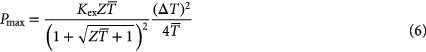
Combining equation (5) with equation (6) yields the required volume of thermoelectric material per generated power
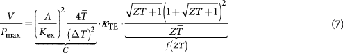
Equation (7) consists of a pre-factor  determined by the operational conditions as these are the external thermal conductance per cross section area of the thermoelectric element
  , the available temperature difference
  and the mean temperature
  , multiplied by a dimensionless function of
  , and also the thermal conductivity of the thermoelectric material
  . This equation allows for a discussion of how changes of
  under an otherwise constant boundary condition affect the volume of the required thermoelectric material per generated power. The explicit occurrence of
  in this equation originates from the thermal matching condition and emphasizes the special role of
  on this ratio. Even for constant
  , the ratio is directly proportional to
  . However,
  is also related to zT. For reasons of simplicity we assume zT =
  by
by

Consequently, one has to distinguish whether a change in  is caused by a change of the power factor
  with constant
  or by a change of
  with constant power factor.
Figure 14(a) presents a contour plot of  normalized to C as function of
  and
and  , while figure 14(b) presents the normalized
  as function of
  either for constant
  or for constant power factor.

Figure 14. (a) 2D-contour plot of the volume per power normalized to pre-factor C of equation (9) as function of  and the thermal conductivity. (b) Double-logarithmic plot of the normalized volume per power as function of
  , either for constant power factor or constant thermal conductivity.
Download figure:
Standard image High-resolution imageIn the range  , there is a strong dependence on
  . For constant
  it scales like

For constant power factor it behaves like

Thus, for  the required volume of material decreases strongly with increasing
  . A lower
  only makes economic sense if the costs for the material and its processing are strongly reduced.
For  the picture is no longer so clear. If the larger
  is obtained by improving the power factor (constant
  ), there is no longer a significant reduction of the ratio
  . Analytically, the curve undergoes a minimum for

At first glance it might seem strange that an increasing  , related with an increasing efficiency, does not require less material per generated power. The reason is that the higher the efficiency, the more the thermoelectric coupling affects the thermal matching condition. In order to fulfill this thermal matching condition, any additional power requires additional volume of thermoelectric material.
An improvement of  in the range
  only makes sense if this is done by lowering of
  . In that case it approximately holds:

Hence, for  , the thermal conductivity is a more crucial parameter than
  itself.
In order to get an impression of the importance of this new measure, power per volume, figure 15(a) summarizes a few thermoelectric materials ordered by their mean zT values compared to the expected power per volume, normalized to the same boundary conditions.

Figure 15. Selected materials ordered by their mean zT value and compared to (a) the power per volume, (b) power per weight and (c) power per cost, all given in relative units under equal boundary conditions.
Download figure:
Standard image High-resolution imageFor this comparison, a cold-side temperature of 100 °C and a hot-side temperature of 600 °C is assumed for all materials, except for Bi2Te3, which is limited to 250 °C. Material data are taken from [26], with the exception of the skutterudites and half-Heusler materials, for which the zT data presented in section 2 was used, i.e. zTav = 1.1 for the skutterudites and zTav = 0.8 for the half-Heusler materials. For the material costs we also refer to [26]. However, since the costs include processing, we have estimated $50 kg−1 as the lower limit for a fully processed thermoelectric material and have accordingly used this value for the silicon-based materials and the half- Heusler materials instead of the lower prices given in [26]. Note that this only corresponds to a very rough estimate since decent cost estimates are difficult to obtain for materials which are still being developed.
Taking the power per volume as a measure for a thermoelectric material, the clathrate becomes much more pronounced compared to its moderate zT value, due to its extremely low thermal conductivity, while the common Bi2Te3 loses due to its limited temperature range.
If one considers the power per weight in figure 15(b), the mass density affects the result further, which now emphasizes the light elements, especially silicon-based materials, while the heavy Bi2Te3 loses again. However, the strongest effect on the 'zT-hit-list' has the material costs—leading to the power per cost parameter, presented in figure 15(c). The very cheap nano-silicon and silicides now become competitive with skutterrudites and half-Heusler compounds, while the clatherate, SiGe-alloy and Bi2Te3 are out of any economically reasonable range for most applications.
While for the comparison between materials the boundary conditions the thermal coupling in particular is assumed to be the same, the absolute costs are also strongly affected by the thermal coupling, expressed by the external thermal conductance per cross section area of the thermoelectric element  . A high external thermal conductance per cross section area is therefore highly appreciated. While it appears in the first instance that
  would be limited by the given heat source and drain, it can be controlled by thermal flux concentration/spreading. This aspect has recently been emphasized by Yazawa and Shakouri [243] by introducing a so called 'fill factor', which is the part of a thermally conducting plate which is covered with thermoelectric material. The thermally conducting plate acts as thermal heat flux concentrator for the heat flux from the source to the thermoelectric material and helps on the cold site to spread the remaining heat flux into the drain. Mostly based on this aspect, they made a first attempt to estimate the cost–efficiency trade-off for thermoelectric modules. Their work indicates further that the thermoelectric material cost is in most cases only a minor part of the total system costs.
3.2. Effective ZT, high operational temperatures and large ΔT
The previous section highlighted the relevance of discussing not only the material's figure of merit but instead the complete thermoelectric generator module (TGM). The importance of tuning the thermal conductivity was pointed out, especially for a material performance that is already in the desirable range of zT > 1.
In the case that the primary energy of the hot side comes for free, as expected for scenarios of waste heat recovery in the medium-high to high temperature regime, thermoelectricity can compete well with other primary energy sources of electricity like nuclear, coal and oil [26]. But this most promising scenario of application requires quite extreme conditions for the operation of TGMs. The high temperature scenario used e.g. by LeBlanc et al [26] for a cost-efficiency analysis of thermoelectric materials operates with a heat source temperature Thot = 800 °C and a sink temperature Tcold = 50 °C. Consequently, ΔT = 750 °C.
Due to the thermal matching conditions needed in order to optimize the dollars per Watt output of the thermoelectric generator, different leg lengths lopt of different materials have to be considered, for instance lopt = 95 mm for nanocrystalline bulk silicon or lopt = 10 mm for skutterudites [26]. The thermomechanical stress the device has to sustain for ΔT = 750 °C can be engineered accordingly only after leg length optimization. Hence, the specific details of the application need to be known before choosing the best possible material.
A quite fundamental aspect of the use of thermoelectricity under large ΔT and high temperature conditions calls into question the conventional thermoelectric device itself. The conventional thermoelectric device as sketched in figure 1 connects n-type legs and p-type legs electrically in series and thermally in parallel. The metallization for the electrical series connection typically consists of several metallic layers, which act as an adhesion layer, inter-diffusion barrier and contact area for the soldering/brazing. The latter connects the semiconductor legs to the two ceramic plates, which serve as a thermal contact to the heat source and sink. Owing to different thermal expansion coefficients of the metal and semiconductor, the hot side metallization is a severe source of device degradation, especially if thermal cycling is applied [245]. High-temperature stable radioisotope TGMs have a different architecture of the couple, optimized for extraterrestrial application. These generators are typically neither cycled nor exposed to oxidizing atmospheric conditions. Hence, the applicability of TGMs for terrestrial use under these extreme conditions needs to be evaluated carefully.
Span et al [246–248] proposed some years ago a thermoelectric generator concept, which eliminates the need for high temperature metallization completely. Instead, this device concept uses a large area pn junction, which is aligned in parallel to the temperature gradient (figure 16). This device concept is especially designed for high hot side temperatures and large ΔT of at least a few hundred degrees celsius—hence applications in the field of industrial waste heat recovery. The fundamental working idea is that at the hot side of the generator, the pn junction is flooded with thermally generated charge carriers and hence does not impose a barrier for the electrical transport across the interface. At the cold side, however, the pn junction blocks effectively and separates the p-type from the n-type region. Besides the fundamental technological advantage of eliminating the metallization, soldering/brazing and also ceramic substrates at the hot end, simulations show that the thermal generation of charge carriers within the pn junction may even help to improve the performance of such a device, finally outperforming the conventional device concepts for large ΔT operation conditions. While experimental data on this device concept are still rare, first proof-of-principle experiments [249, 250] suggest that this device concept might actually open a novel path towards a high temperature design of thermoelectric waste heat recovery systems, especially for the use of radiation heat.

Figure 16. Schematic of the pn-TEG architecture shows that only the cold side substrate and metallization are required.
Download figure:
Standard image High-resolution imageExperimentally, it is common that the transport coefficients σ, κ, α, are measured with ΔT = 0 or a small ΔT, which are not the operating conditions of the thermoelectric materials or modules. The large ΔT condition opens another, maybe more academic question because the figure of merit is derived in context of a constant property model. However when ΔT goes above a few hundred degrees celsius it is clear that the transport coefficients along the material cannot be treated as constants, hence, what is the effective zTeff under large ΔT? Although there does not seem to be a robust consensus about how to handle this issue, one natural approach is to average the transport coefficients over ΔT, as Borrego has done, and write an effective figure of merit as [251]
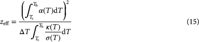
It seems that Borrego's approach points in the right direction. However, he did not consider the Thomson effect. More recently, Min and Rowe considered the Thomson effect and developed a method to measure zT under large ΔT arriving at the following expression [252–254]
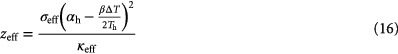
Here  is the effective electrical conductivity,
  the local Seebeck coefficient at the hot side interface, β the Thomson coefficient and
  the effective thermal conductivity. Similar to the Harman technique, the method developed by Min and Rowe provides an elegant way to measure the figure of merit based on electrical currents and voltages, however their method fails to explain experimental data [252–254].
Another approach to attack the issue of temperature dependent coefficients is the 'compatibility approach' introduced by Snyder and Ursell [255], and later developed by Seifert et al [256, 257]. In this approach the starting point for the efficiency consideration takes a general form that does not require assumptions of near equilibrium conditions [255]:
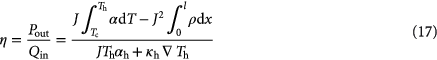
Here J is the electric current density, ρ the resistivity and the subscript h indicates the hot side boundary. The compatibility approach was developed for segmented thermoelectrics where the materials are locally optimized for the temperature in which they operate. However, a homogeneous material under a large temperature gradient can be considered as a type of a segmented material. The compatibility approach is oriented to find the optimal segmentation of the thermoelectric leg and it would be interesting to find the optimal temperature difference for a homogeneous material.
3.3. Novel directions for thermoelectric research
A novel device concept like the pn junction TEG (figure 16) can, thermodynamically speaking, be interpreted as a change of the thermodynamic engine: a thermodynamic analogy between the thermoelectric engine and traditional steam engines was first proposed by Vining [258] and followed up by Goupil et al [25] and Shakouri [259]. In the analogy, entropy is transported by a gas in both systems; in the thermoelectrics domain the gas is a 'Fermi Gas', i.e. a gas of electrons, where a temperature T describes the system and an electrochemical potential μ. While in the gas cycle domain, the gas is an ideal molecular gas described by a temperature T and a pressure P. Vining showed that the maximum conversion efficiency of the thermoelectric process can be written as:
and has a conjugate in the gas cycle domain.  and
and  is the open circuit thermal conductivity and
  is the closed circuit thermal conductivity. In a gas cycle consisting of two constant pressure steps and two constant volume steps (dPdV), a similar expression for the maximum efficiency can be obtained:
where  and CP is the constant pressure specific heat and CV the constant volume specific heat. The analogy between the thermoelectric process and a gas cycle described above is evident in the similarities between equations (18) and (19), and from the units of
  and
and  which are in terms of energy transfer or energy absorption per Kelvin.
In the gas cycle domain, there are three main strategies to improve the conversion efficiency: (i) search for the gas with the highest  ratio, (ii) search for a gas that exhibits a phase transition such as Freon 12 as shown in figure 17, or (iii) change the gas cycle or engine. Each of these strategies translates to the following in the thermoelectrics domain: (i) changing the working gas is equivalent to searching for materials with high zT value; (ii) searching for a gas that exhibits a phase transition is equivalent to searching for materials with a purely electronic phase transition, and (iii) changing the gas cycle or engine is equivalent to searching to modify the thermoelectric process.

Figure 17. Specific heat ratio  for a PV system (Freon 12) and thermal conductivity ratios
  for selected n-type alloys. Redrawn after Vining [258] with permission from Cambridge University Press.
Download figure:
Standard image High-resolution image
Possible indications for the last strategy have been discussed above [249, 250] where pn junctions have been demonstrated to work as thermoelectric engines which cannot be described by the traditional figure of merit zT, hence, providing evidence that different thermoelectric 'engines' are possible.
Of course, looking at figure 17, the chance of finding a material which offers a purely electronic (but not structural) phase transition seems to be even more inspiring than optimizing the thermoelectric figure of merit or redesigning the thermoelectric engine.
4. Conclusion
Medium-high to high temperature waste heat recovery is an interesting potential application of thermoelectric materials. We reviewed the thermoelectric properties of three families of thermoelectric materials which target this temperature regime and whose development is close to the requirements of commercialization, namely skutterudites, half-Heusler compounds and silicon-based materials. They already fulfill most of the industrial demands for TE materials, i.e. environmental-friendliness, low cost and availability of raw materials, long-term stability, producibility in industrial quantity and chemical and mechanical resistance at high temperatures.
Skutterudites allow for a wide tuning of the electronic properties such as the band gap and position of the Fermi level at the electronic density of states by designing the composition of the solid solution combined with nanostructuring. Attractive zT values (zT ~ 1.2 for p- and zT ~ 1.7 for n-type skutterudites) reaching thermoelectric conversion efficiencies of about 14% (for a single leg) in the medium-high temperature range (RT to 550 °C) characteristic for automotive applications were shown. The half-Heusler compounds employ phase separations as an important tool in the design of highly efficient thermoelectric materials. Their attractive properties for thermoelectric applications are high Seebeck coefficients up to ≈300 µVK−1 at room temperature and high electrical conductivity (≈1000–10 000 Scm−1), but combined with a relatively high thermal conductivity. zT values of >1 are reproducibly possible. Silicon and silicon-based alloys and composites are highly desirable for thermoelectric applications with respect to costs and sustainability of the raw material, as well as fabrication techniques, e.g. scalable gas phase synthesis of the nanopowder. By alloying nanobulk silicon with only a few percent of germanium, the figure of merit of both n-type and p-type SiGe alloys is in the desirable range of zT ~ 1. Highest zT values of 0.7 for nanobulk n-type silicon (without any alloying) were shown. For n-type compositions of magnesium silicide based solid solutions, zT values >1 were demonstrated.
In principle, all modules need to be designed exclusively for the required application. It was discussed that the efficiency (and with it the figure of merit, zT) is only an important parameter if the primary energy has already a price, which is transformed by the efficiency into a price of the secondary energy. But, if the primary energy is available as energy flux without costs, for example solar radiation, wind power or waste heat, the cost per provided power ($ per Watt) becomes a measure for the economic evaluation. Accordingly, the physics of the energy transformation process was analyzed, to allow for an estimation of the required amount of material in order to generate a specific amount of power. Consequently, the question of cost per power is shifted to the question of costs for the required material. Applying this analysis to different thermoelectric materials puts the zT data into perspective, since expected power per volume, per weight or per cost of the material are extracted as even more relevant parameters for an application in the waste heat recovery scenario. Hence, while for instance the zT data of nanobulk silicon cannot compete with those of the skutterudites and half-Heusler compounds presented here, the expected power per cost lets it become a competitive player.
We further discussed novel device architecture, which may be better suited to the recovery of radiation heat than the conventional thermoelectric generator module. TEGs which use a large area pn junction, which is aligned in parallel to the temperature gradient, are especially suitable for high hot side temperatures and large ΔT of at least a few hundred degrees Celsuis—hence applications in the field of industrial waste heat recovery. This new kind of 'thermoelectric engine' offers the fundamental technological advantage of eliminating the hot side metallization, soldering and also ceramic substrates. Simulations give rise to the hope that the efficiency of such devices reaches (or under certain conditions outperforms) the efficiency of standard TEGs, and first proof-of-principle experiments indicate that this device concept might actually open a novel path towards a high temperature design of thermoelectric waste heat recovery systems.
Acknowledgment
GS acknowledges a young investigator grant co-financed by the University of Duisburg-Essen and the State of North-Rhine Westphalia, Ministry for innovation, science and research.
Footnotes
- 5
Table of cost values associated with Figure 5(c,d) in S LeBlanc, S K Yee, M L Scullin, C Dames, K E Goodson, "Material and Manufacturing Cost Considerations for Thermoelectrics," Renewable & Sustainable Energy Reviews, February 2014. Compiled by Dr Saniya LeBlanc, The George Washington University for Dr Gabi Schierning, Universität Duisburg – Essen, July 2014.
Biographies

Gabi Schierning studied Materials Science and Engineering at the University of Erlangen-Nuremberg, Germany, where she received her diploma degree in 2002. She obtained her PhD degree from the same University in 2005 under the supervision of Albrecht Winnacker. After Post-Doc positions at the Technical University of Darmstadt and the Karlsruhe Institute of Technology, she joined Roland Schmechel's group at University of Duisburg-Essen in 2007. Since 2009, she has been group leader of an independent young researcher group working on nanostructured thermoelectric materials at University of Duisburg-Essen. In 2014, she was awarded the Innovationspreis of the State of North-Rhine Westphalia in the category 'young scientist' for her work on nanostructured bulk silicon for thermoelectric application.

Benjamin Balke finished his PhD under the supervision of Prof Claudia Felser at the Johannes Gutenberg-University Mainz in 2008. Thereafter, he worked as a Feodor Lynen Research Fellow in the group of Prof Fadley (Lawrence Berkeley National Laboratory) and in the group of Prof Ramesh (UC Berkeley) in Berkeley, CA, USA. Since April 2009 he is the group leader of Thermoelectrics and Solid State Chemistry at the JGU in Mainz. His present research is focused on the design of Heusler compounds with large spin–orbit coupling for spintronic applications and the design of Heusler compounds for thermoelectric applications, in particular the design of intrinsic phase separations to enhance the thermoelectric figure of merit.

Gerda Rogl (MSc in Mathematics and Physics 1969, University of Vienna) worked as high school teacher for more than 30 years, editing 2 schoolbooks during this time. She started PhD work in January 2008, obtained her PhD degree in Physics (University Vienna), focusing on skutterudites, nanocrystallization, mechanical properties, severe plastic deformation. G Rogl has authored/coauthored 35 articles in peer reviewed journals and 1 chapter in a book.

Peter Franz Rogl (degree in physics from the University of Vienna, 1971); postdoctoral research associate at the Oregon Graduate Center for Study and Research (1974–1976); venia docendi in Physical Chemistry (1980) and aO Prof 1986, both at the Institute of Physical Chemistry, University of Vienna. Since 2004 he is a full professor at the chair of Physical Chemistry of Materials (University of Vienna). In 2000 P F Rogl became an honorary professor at the Northeastern University of Shenyang. P R was awarded the Sandoz research award 1985 of the Sandoz Research Center and the Felix Kuschenitz Price 1992 of the Austrian Academy of Sciences for outstanding research. P F Rogl has authored/co-authored more than 600 articles in peer reviewed journals and 22 books or chapters in books.