
Abstract
Based on first-principles calculations, the electronic properties of a black AsP monolayer were investigated by applying an external strain. It was found that the electronic property and effective mass of black AsP monolayer exhibits strong anisotropy. Comparing with the armchair direction, the zigzag direction was more resistant to elastic deformation. When the strain was applied along the zigzag direction, a direct-indirect-direct transition of the band gap occurred with increasing tensile strain and compressive strain. The direct to indirect transition occurred at a −2% compressive strain when the strain was applied along the armchair direction. The direct-indirect transition occurred at biaxial compressive and tensile stains of −3% and 3%, respectively. In addition, the effective mass of electrons and holes along the armchair direction is an order of magnitude smaller than that associated with the zigzag direction, suggesting that electron and hole transport will occur preferentially along the armchair direction. Moreover, we found that the effective mass of the black AsP monolayer can be significantly tuned by strain.
Export citation and abstract BibTeX RIS

Original content from this work may be used under the terms of the Creative Commons Attribution 4.0 licence. Any further distribution of this work must maintain attribution to the author(s) and the title of the work, journal citation and DOI.
1. Introduction
In recent years, two-dimensional (2D) materials [1] have garnered widespread attention due to their excellent properties. Graphene [2–4], a typical example of such materials, exhibits high electrical conductivity and high carrier mobility, and is therefore a potential candidate for use in nanoelectronic applications. However, the zero band gap of graphene has limited its applications. Therefore, several studies have focused on developing other 2D layer materials (e.g., transition metal dichalcogenides [5, 6] MXenes [7, 8] phosphorene [9, 10] and indium selenide [11, 12]), which exhibit novel electronic and optical properties required for next-generation optoelectronic devices.
Phosphorene, a puckered structure black phosphorus monolayer that is characterized by a moderate direct band gap, exhibits high in-plain anisotropy, quite high carrier mobility, and promise for unique application prospects in optoelectronic devices. For example, Zhang et al [13] developed black phosphorus field-effect transistors. After the successful synthesis of phosphorene [14], monoelemental compounds of group VA, involving arsenene, antimonene, and bismuthene [15–18] and group IV−VI monochalcogenide monolayers [19–22] with similar structure to that of phosphorene, have attracted considerable attention. Previous research has revealed the high carrier mobility [23] and excellent thermoelectric performance [24] of α-arsenene, indicating the potentially broad application prospects of this material in optoelectronic devices and thermoelectric devices. Previous study found that 2D GeSe exhibits significant promise for use in high performance thin-film solar cells [25]. The work in our group predicted that 2D GeSe/SnSe heterostructures has high photoelectric conversion efficiency, which is a potential candidate for solar cells [26]. Furthermore, 2D V-V binary compounds [27–29] have attracted considerable attention, owing to the unique properties of group VA monoelements. Qu et al [30–32] found that the strong anisotropic electronic structure including effective mass and density of state in 2D group VA-VA monolayers is helpful for designing high performance 2D field effect transistors. This is especially true for black arsenic phosphorus monolayers, which are considered a potential donor material for 2D solar cells [33]. Black arsenic phosphorus can be used to detect mid-infrared spectra at room temperature and exhibits high performance detection efficiency [34] suggesting that this material is suitable for nanoelectronic applications.
Several studies have focused on modifying the electronic and optical properties of 2D materials by appling strain, external fields, doping, defects, chemical functionalization, and heterostructures [35–40]. Among them, applying an external strain is one of practical approaches. In this work, the effect of strain on the mechanical and electronic properties of monolayer black arsenic phosphide (AsP) is explored systematically based on first-principles calculations. The Poisson's ratio, change in the total energy, band gap, and effective mass under strain are discussed. The results revealed that the band gap value and type can be tuned by in-plain strain. More importantly, the effective mass of carriers in a black AsP monolayer can be tuned significantly by strain, thereby allowing tuning of the carrier mobility.
2. Computational details
The Vienna ab initio simulation package [41, 42] (VASP) was used to perform first-principles calculations under the framework of density functional theory [43] (DFT). The generalized gradient approximation [44, 45] (GGA) of the Perdew, Burke, and Ernzerhof (PBE) functional [46] was used to describe the exchange correlation interaction. A cutoff energy of 500 eV was adopted for the plane wave basis vector. A 14 × 11 k point mesh was adopted for 2D Brillouin zone sampling. To eliminate the periodic interaction between neighboring cells, a thickness larger than 20Å was adopted for the vacuum layer along the z direction. The lattice constants and the ionic positions were fully optimized until accuracy levels of 10–6 eV and 0.01 eV A−1 were realized for the energy and force, respectively. To avoid underestimation of the band gap by the PBE functional, a more accurate HSE06 hybrid functional (than the conventional functional) was used in our calculations. The exerting strain was defined as εx ax-ax0/ax0, εy = ay-ay0/ay0; εxy corresponded to a strain that was simultaneously applied in the x direction and y direction. In addition, εx:εy = 1:1 was adopted, where ax(ay) and ax0(ay0) are the lattice constants strained and unstrained along the x(y) direction, respectively. We considered both uniaxial and biaxial strains ranging from −10% to 10%. The positive values of strain corresponded to expansion, while the negative values denoted compression. For energy minimization during uniaxial straining, we fixed the lattice along the strain direction and optimized the lattice along the lateral direction.
3. Results and discussion
3.1. Geometric configuration and electronic properties of black AsP monolayer
The black AsP monolayer has an orthorhombic lattice with a space group of Pmna2, which is similar to that of phosphorene, a unit cell containing four atoms with alternating P atoms and As atoms (see figure 1).
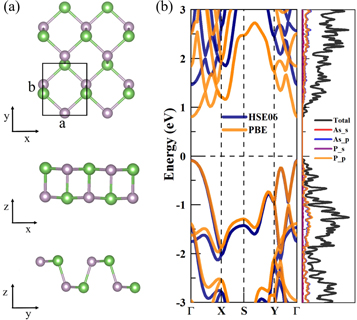
Figure 1. Atomic configuration view along (a) x-y axis (b) y-z axis (c) x-z axis (d) the band structure (PBE method and HSE06 method) and project density of state (PBE method) of black AsP monolayer.
Download figure:
Standard image High-resolution imageFurthermore, the optimized lattice constants of the monolayer are a = 3.50 Å, b = 4.69 Å, which are consistent with previous DFT calculations [33]. The band structure and projected density of states (PDOS) are presented in figure 1(d). The band structure calculations are performed using the PBE method and HSE06 method, which yield band gap values of 0.90 eV and 1.55 eV, respectively. These results are consistent with previous reported findings [33]. From the PDOS image, we observe that the contributions of the valence band maximum (VBM) and the conduction band minimum (CBM) arise mainly from the 3p state of the P atom and the 4p state of the As atom. This similarity results from the similar electronegativities of the P atom and As atom as well as the strong hybridization of the 3p orbital comprising the P atom and the 4p orbital comprising the As atom.
3.2. Poisson's ratio and changes in the total energy of monolayer AsP under strain
Generally, for 2D materials stretched in the axial direction, shrinkage deformation occurs along the direction perpendicular to the material. Poisson's ratio, which is given as  reflects the elastic constant of transverse deformation in the material. The relationship between the transverse strain and the axial strain is plotted in figure 2(a) (Poisson's ratio values for the zigzag and armchair directions are 0.23 and 1.01, respectively). The significant difference between the ratios indicates the anisotropy of the black AsP monolayer. The Poisson's ratio of the monolayer is slightly lower than that of phosphorene along the zigzag direction, and slightly greater than that of phosphorene along the armchair direction [47]. The axial-strain-induced changes in the total energy of the monolayer are plotted in figure 2(b). As shown in the figure, the applied axial strain along the zigzag direction results in greater changes than the strain applied along the armchair direction, indicating that the zigzag direction is more resistant to elastic deformation. That is, the strain applied along the zigzag direction has the least effect on the structural stability of the material.
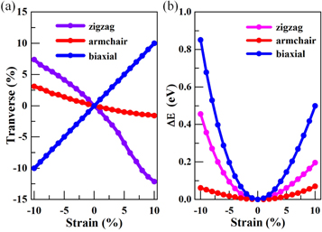
Figure 2. (a) The applied axial strains along the x and y axis and their transverse strain response along the y and x directions, respectively. (b) The change of the total energy as a function of the applied strain.
Download figure:
Standard image High-resolution image3.3. Band gap of black AsP monolayer under strain
To obtain more accurate band gap results (than those previously reported), a hybrid functional HSE06 method is used in our calculations. The relationship between the band gap and strain is revealed in figure 3. For strain applied along the zigzag direction, the band gap decreases linearly with increasing compressive strain until a strain value of −9% is reached. The gap value decreases sharply when a strain of −10% is reached. However, for increasing tensile strain, the value increases slightly at first, and then occurs either under compressive strain or tensile strain. For strain (−10% to 10%) applied along the armchair direction, the value of band gap increases monotonically. Furthermore, the band gap of black AsP monolayer exhibits a decreases linearly with increasing compressive strain. In contrast, the band gap is monotonous increasing along with the increasing tensile strain. A direct-indirect conversion in band gap is occur for strain values less than −2%. For the applied biaxial strain, the band gap value decreases substantially with increasing compressive strain. The value increases linearly, however, with increasing tensile strain until a strain value of 3% is reached, and decreases rapidly thereafter. The maximum gap value of 1.85 eV is obtained at a strain value of 3%. The direct band gap is maintained for compressive and tensile strain values of ≤2%, and the indirect band gap occurs for strains of >2%. In order to reveal the variation trend of CBM and VBM of black AsP monolayer in black AsP monolayer along with the applied tensile or compressive strain, in figure S1 (available online at stacks.iop.org/MRX/9/025009/mmedia) of the supplementary material, we show the CBM and VBM of black AsP monolayer under the applied strain. It implies that the band gap of black AsP monolayer exhibits anisotropy character under the applied uniaxial strain, which is decided by the relative energy level of CBM and VBM. This is induced by the different structural deformation of the AsP monolayer induced by the applied strain along different directions or by applying biaxial strain.
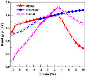
Figure 3. Band gap variations of black AsP monolayer under uniaxial (zigzag direction and armchair direction) and biaxial strain. The solid and hollow icons represent direct and indirect band gap, respectively.
Download figure:
Standard image High-resolution image3.4. Band structure of black AsP monolayer under strain
The influence of strain on the electronic properties of monolayer black AsP is further explored by plotting the band structure at some specific strain (see figure 4). For intrinsic monolayer black AsP, we observe a direct band gap resulting from the CBM and VBM located on the Γ point. Consider a strain applied along the zigzag direction. When the applied compressive strain increases to −3%, we found that the CBM and VBM are still located on this point but the band gap decreases to 1.47 eV. Moreover, the CBM moves slowly toward the Fermi level. The band gap decreases to 1.09 eV when the material is subjected to a compressive strain of −10%, and the CBM moves further toward the Fermi level. When a tensile strain of 3% is applied, the VBM moves from the Γ point to a k point on the Γ-Y path, and the distance between the CBM and the Fermi level changes only slightly. Considering an applied tensile strain of up to 10%, owing to this strain, the CBM moves from the Γ point to the Γ-Y path, a direct band gap of 0.57 eV is formed, and the energy between the CBM and the Fermi level decreases further. These results indicate that the CBM is more sensitive to tensile strain than to compressive strain. Furthermore, monolayer black AsP exhibits semiconductor characteristics over the strain range (−10% to 10%) considered (for strain applied along the y axis and xy axis, see figure S2 for more details). To better understand the change of VBM and CBM in the band structure under different applied strain, we give a more detailed analysis on the variation of VBM and CBM tuned by in-plane strain along x, y and biaxial directions, which can be found in figures S3 and S4 in supplementay material.
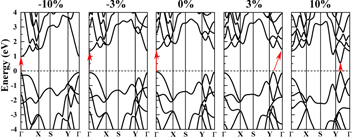
Figure 4. Electronic band structure of black AsP monolayer subjected to strain of −10%, −3%, 0%, 3%, and 10% along the x axis.
Download figure:
Standard image High-resolution image3.5. Effective mass of black AsP monolayer under strain
Previous studies have demonstrated that strain has a significant impact on the transport properties of 2D materials. The carrier mobility plays a critical role in the performance of measurement devices, and the carrier mobility is inversely proportional to the effective mass of electrons and holes. Therefore, we explore the effective mass of electrons and holes under both axial strain and biaxial strain. The effective mass is calculated as follows:  For intrinsic monolayer black AsP, along the zigzag (Γ-X) direction, effective mass values of 1.226 m0 and 2.040 m0 are obtained for the electrons and holes, respectively. However, in the armchair (Γ-Y) direction, mass values of 0.179 m0 and 0.157 m0 are obtained for the electrons and holes, respectively. These results are consistent with those of a previous study [30]. In figure 5, the relationship between the effective mass of electrons and holes and the strain is illustrated for strain applied along the x direction.
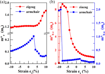
Figure 5. Effective masses of (a) electron and (b) hole as a function of uniaxial strain εx.
Download figure:
Standard image High-resolution imageWe observe from figure 5(a) that the effective mass of electrons along the zigzag direction changes only slightly under compressive strains, indicating that the mass insensitive to strain in this case. However, along the armchair direction, the effective mass increases initially and then decreases with increasing tensile strain, with a sudden drop resulting from the CBM jumping from the Γ point to the Γ-Y path. A detailed band structure showing all the effective mass sharp jump/drop points is presented in figure S5. In figure 5(b), the effective mass of the holes along the zigzag direction changes significantly under compressive strain, demonstrating that this mass is sensitive to strain. Moreover, the jump occurs at −10% compressive strain and −9% compressive strain along the zigzag direction and the armchair direction, respectively. This considerable change results from the fact that the band dispersion is weak along the Γ-Y direction around VBM. For strains of up to −9%, the dispersion is enhanced along the Γ-X direction around VBM when the strain reaches −10%.
For strain applied along the y direction, with increasing compressive strain, the effective mass of electrons exhibits the same trend along the zigzag direction and the armchair direction (figure 6(a)). However, the mass is insensitive to the tensile strain along these directions. Due to the strain-dependent sensitivity of the VBM, the effective mass of the holes exhibits irregular variation
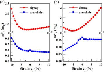
Figure 6. Effective masses of (a) electrons and (b) holes as a function of uniaxial strain εy.
Download figure:
Standard image High-resolution imagealong the zigzag direction (figure 6(b)). The effective mass of electrons along the armchair direction is an order of magnitude smaller than that along the zigzag direction, for strain ranging from −10% to 10%. This indicates that electron transport will occur preferentially along the armchair direction.
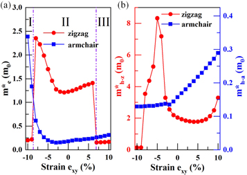
Considering the application of strain in biaxial directions, at a compressive strain of −9% and a tensile strain of 7%, the effective mass of electrons decreases sharply along the zigzag direction (see figure 7(a)). This results from the jump of CBM from the Γ point to the Γ-X path and enhanced band dispersion in the Γ-X direction around CBM. In addition, the effective mass of electrons along the armchair direction is more sensitive to larger compressive strains than to smaller compressive strains. These results indicate that the electrons in region I and region II are mainly transported along the zigzag direction and the armchair direction, respectively. The effective mass of holes is sensitive to compressive strain along the zigzag direction and a sudden drop occurs at a compressive strain of −9% (see figure 7(b)). This drop results from enhancement of the band dispersion in the Γ-X direction around VBM (the corresponding band structure is presented in the supplementary material (figure S2)). This change leads to a competition between the hole transport along the armchair and that along the zigzag direction. However, for strains ranging from −9% to 10%, this transport occurs preferentially along the zigzag direction. In the literature, carrier effective mass in many other 2D materials were reported. For example, in black phosphorene, it was reported that its carrier effective mass is anisotropic with an hole/electron mass of 11.16m0/1.24m0 close to the Γ point (VBM) and a hole/electron mass of 0.14m0/0.15m0 along the Γ-Y direction [48]. Similar anisotropic behavior was also found in 2D semiconductor GeP by first-principles prediction [49]. Some of them were also sensitive to the applied external strain. For example, in MSb (M = C, Si, Ge and Sn) monolayers, it was found that the effective mass can be tuned by applying strain [50]. In our recent study of 2D PbSe [51], we also found that the effective mass of both electron and hole can be tuned by biaxial strain. In table S1 in supplementary material, we list some values of effective mass of electron and hole under some particular applied strains. It implies that the external in-plane strain is an efficient way to tune the effective mass of electron and hole in 2D AsP.
Figure 7. Effective masses of (a) electrons and (b) holes as a function of biaxial strain εxy.
Download figure:
Standard image High-resolution image
4. Conclusions
Using first-principles calculations, we systematically investigated the effect of strain on the electronic properties of a black AsP monolayer. This monolayer is characterized by a direct band gap, which is quite desirable for optical applications. We found that AsP monolayer exhibits strong anisotropy and the ability to resist elastic deformation along the zigzag direction than that along the armchair direction. The transition of the band gap from direct to indirect occurs for both axial and biaxial strain within the applied strain range. Our predicted results indicate that the effective mass can be significantly tuned by strain, thereby allowing tuning of the carrier mobility. Our results can serve as a reference for the use of black AsP monolayers in electronics applications.
Acknowledgments
This research is funded by Natural Science Foundation of Hunan Province, China (Grant No. 2021JJ30650) and National Natural Science Foundation of China (Grant Nos. 11374251, 11471280).
Data availability statement
The data generated and/or analysed during the current study are not publicly available for legal/ethical reasons but are available from the corresponding author on reasonable request.