

Abstract
Reactive magnetron sputtering deposition of nickel oxide (NiO) films were done on p-type silicon substrate and glass substrate under Ar+O2 gas environment at substrate temperature of 26 °C, 100 °C, 200 °C and 300 °C. The phase, crystallinity and grain size were analysed by x-ray diffraction in grazing incidence mode (GIXRD). The average grain size varied in the range of 12 nm to 28 nm for NiO films. The microstructural analysis was carried out under a field emission scanning electron microscopy (FESEM) as well as transmission electron microscopy (TEM). Uniform distribution of grains and lower surface roughness were observed for the NiO films processed at relatively higher temperature. Direct band gap of investigated NiO films were measured with the help of absorption data obtained from UV-visible photospectrometer. The direct band gap was found to vary from ≈2.92 eV to ≈3.96 eV with change in substrate temperature.
Export citation and abstract BibTeX RIS
1. Introduction
Recently nanocrystalline NiO thin films have gain significant importance due to its potential applications in the area of semiconductor solar cells, sensors, supercapacitor, spintronics, automobile industry and aerospace because of its very good electrical, optical and magnetic properties as well as outstanding chemical stability [1–5]. In addition to that NiO thin films are also recognized as a p-type semiconductor with direct band gap varying in the range of 3.6 eV to 4.0 eV [6, 7] which makes these films more important for the potential application as an oxide for metal-oxide-semiconductor (MOS) devices.
In past NiO films were processed by various chemical and physical vapour deposition techniques such as spray pyrolysis, electrochemical deposition, thermal evaporation, chemical solution deposition and magnetron sputtering [8–19]. Among the mentioned techniques, magnetron sputtering is the most versatile technique for nanocrytalline nickel oxide thin film deposition. In this technique purity of the processed films can be easily controlled by controlling the purity of the gases, vacuum level of sputtering chamber, quality of substrates and target materials used for deposition. Further surface morphology and grain size distribution can be regulated by monitoring magnetron sputter related parameters like substrate bias, substrate temperature, target power etc [20–23].
Results of literature survey show that metal oxide films have been mainly studied for application in bio/chemical sensors, semiconductor devices, photo catalytic activities etc because of its excellent electrical properties, very good optical properties and its chemical stability [24–27]. Hotovy et al [28] have studied the electrical properties of reactively dc magnetron sputtered NiO thin films. In this study, it has been observed that electrical resistivity increases with increase in oxygen content in the NiO films. Chen et al [29] have observed the change in crystallographic orientation of sputtered NiO films with variation in Argon to oxygen gas ratio at different substrate temperature. Further Chen et al [16] have reported the effect of magnetron sputtering related parameters on the electrical and optical properties of NiO thin films. Raut et al [30] have prepared the NiO films using sol-gel spin coating method. They have reported that the dc electrical resistivity decreases with increase in the annealing temperature of the deposited NiO films. In another study, the gas sensing ability of NiO films has been observed [31]. Recently, Zhao et al [32] have investigated the effect of oxygen partial pressure on the structural, optical and electrical properties of NiO films grown by radio frequency magnetron sputtering. Most recently, Zhao et al [33] have reported the effect of growth temperature on the electrical and optical properties of rf magnetron sputtered nickel oxide films. From literature survey it is intuitive that properties of the NiO films depend upon the processing parameters like substrate temperature, substrate bias, oxygen partial pressure etc Therefore, in the present investigation NiO films have been processed by reactive dc magnetron sputtering at different substrate temperatures in order to tailor the desired surface morphology and direct band gap.
2. Experimental
2.1. Processing
A DC magnetron sputtering system (model KVS-T 4065, Korea Vacuum Tech.) consists with Nias a target material was used to grow on p-type Si (100) substrates as well as on glass substrate NiO films under 99.99% pure Ar + O2 gas environment. Before deposition a base pressure of order 2 × 10⁻⁶ Torr were achieved by a rotary and turbo-molecular pump. The flow rate of Ar and O2 gas were controlled using mass flow controllers, whereas the chamber pressure was measured using an MKS Baraton gauge. During deposition substrate was heated at various temperatures such as room temperature (26 °C), 100 °C, 200 °C and 300 °C with the help of winded SiC heating element fitted just below the substrate holder. Other relevant processing parameters used for deposition of the NiO films are shown in table 1.
Table 1. Processing parameters used for magnetron sputter deposition of NiO films.
| Processing parameters | Values |
|---|---|
| Base pressure | 2.0 × 10⁻⁶ Torr |
| Working pressure | 30 mTorr |
| Ar:O2 | 1:1 |
| Ar and O2 flow rate | 50 sccm |
| Ni DC Power | 50 W |
| Substrate temperature | 26 °C, 100 °C, 200 °C and 300 °C |
| Substrate bias | 0 V |
| Substrate Rotation Speed | 25 rpm |
| Substrate to Target distance | 150 mm |
| Duration for deposition | 1 hour |
2.2. Characterization
The NiO films thichkness were measured by surface profilometer (Dektak 150 surface profiler, USA). The phase and crystallinity of the NiO films deposited at different substrate temperature were analysed x-ray diffraction in grazing incidence mode (GIXRD) (Philips X'Pert PRO Diffractometer) which was operated at 30 mA current and 40 kV of accelerating voltage. The GIXRD scans were done in the range of 32° to 72° with scan rate 0.05 °/s using Cu Kα radiation (wavelength = 0.154 nm). The GIXRD peaks were also used to measure the value of average grain sizes using the Williamson-Hall relationship [34]. A field emission scanning electron microscope (FESEM) (Model: Zeiss SUPRA 40) were used for the microstructural analysis of the investigated NiO thin films. During microstructural studies, chemical compositions were also measured by an energy dispersive x-ray (EDX) microanalyzer attached with the same FESEM. Further detail analysis of microstructure was done using a transmission electron microscopy (JEOL-JEM 2100). For this purpose cross-sectional samples were prepared by mechanical thinner using a dimpler (Model 656 Gatan Inc.) followed by Ar+ ion-milling (model 691, Gatan Inc.) with ion beam energy of 4.8 keV. During microstructural analysis on TEM, micrographs were captured in both bright and dark field imaging modes. At the same time selected area diffraction pattern (SEAD) was captured for the analysis of phases present in the investigated sample. Absorbance spectra of the investigated NiO films were obtained by UV-visible double beam photospectrometer in the wavelength range of 300 nm to 1000 nm. Uncoated glass slide was taken as reference sample for UV-photospectrometer data analysis.
3. Results and discussion
3.1. Effect of substrate temperature on deposition rate
The average thickness for the NiO films deposited at different substrate temperature has been measured by surface profilometer varies from 480 nm to 400 nm. The variation of average deposition rate of NiO films with substrate temperature is shown in figure 1, which shows marginal decrease in deposition rate with increase in substrate temperature. It may be due to both decrease in formation of island land per unit substrate area and desorption of adatoms from the growing surfaces [22, 35]. As substrate temperature increases the nucleation density or number of formation of islands decreases due to increase in adatom mobility and the desorption rate of the sputtered atoms received at depositing substrate increases which leads to lower sticking efficiency of adatoms on growing islands. Moreover, desorption rate of physio-absorbed nickel and oxygen adatoms increases with increase in substrate temperature but at the same time this phenomenon restricted by formation of nickel oxide by chemical reaction between nickel and oxygen atoms.
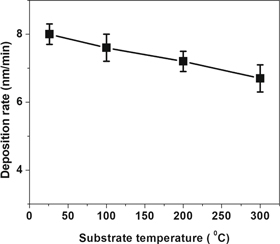
Figure 1. Variation of deposition rates of NiO films deposited at different substrate temperature.
Download figure:
Standard image High-resolution image3.2. XRD analysis
The XRD results analysis of the NiO films deposited at different substrate temperature such as room temperature (26 °C), 100 °C, 200 °C and 300 °C are shown in figure 2. This shows the presence of nanocrystalline NiO phase having face centred cubic (FCC) structure matches with the ICDD data base (PDF # 47-1049) with 〈111〉 direction as preferred orientation for the reactively sputter deposited thin films. The preferred orientation 〈111〉 becomes stronger with increase in substrate temperature because this orientation leads to minimum surface energy which may also enhance the growth rate of NiO thin films. In another study, It has been reported that 〈111〉 orientation as a preferred orientation for NiO films deposited under low ratio of oxygen (<50%) at relatively lower temperature (<200 °C) because this orientation accommodate maximum number of NiO molecules in (111) planes which helps in minimizing surface energy. However, 〈111〉 orientation as preferred orientation has been observed for the NiO films processed under pure oxygen atmosphere (100%) and higher substrate temperature (>400 °C) [29]. The average grain sizes and RMS value of the microstrain developed in the NiO films were measured using Williamson-Hall relationship [34] are given in table 2. It shows the increase in grain size of NiO with increase in substrate temperature which may be attributed due to decrease in rate of nucleation site formation because of increase in adatoms mobility. Further microstrain developed in the NiO films is found to decrease with increase in substrate temperature because of more uniform deposition at relatively higher temperature.
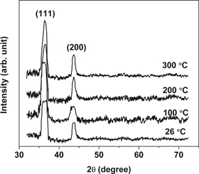
Figure 2. GIXRD patterns of the NiO films deposited at different substrate temperature.
Download figure:
Standard image High-resolution imageTable 2. Grain size and RMS strain obtained for nanocrystallineNiO films deposited at different substrate temperature.
| Substrate temperature (°C) | RMS strain (X 10−3) | Grain size (nm) |
|---|---|---|
| 26 | 3.5 ± 0.5 | 12.6 ± 0.6 |
| 100 | 2.9 ± 0.6 | 15.4 ± 0.4 |
| 200 | 2.5 ± 0.4 | 22.5 ± 0.5 |
| 300 | 2.1 ± 0.4 | 28.4 ± 0.3 |
3.3. Microstructural and elemental analysis
The FESEM micrographs of the NiO films deposited at room temperature, 100 °C, 200 °C and 300 °C are shown in the figures 3(a)–(d), respectively. NiO films deposited at room temperature possess agglomerated surface morphology with smaller grain size (figure 3(a)) while the NiO films deposited at higher substrate temperature consists of comparatively smoother surfaces and larger grains (figures 3(b)–(d)). Agglomeration in microstructures takes place because of the limited adatoms mobility on the depositing surface at lower temperature. As substrate temperature increases adatoms mobility also get increases which leads to decrease in rate of formation of nucleation sites causes increase in grain size with uniform distribution over the substrate surface. During FESEM micrographs analysis, energy dispersive spectroscopy (EDS) analysis has also been done to locate the position enrichment of Ni and O elements in the NiO thin films. Bright and dark field images along with a representative SAED pattern captured on TEM for the NiO films deposited at 100 °C are shown in the figures 4(a)–(c), respectively. TEM bright field image (figure 4(a)) shows the more or less equiaxed microstructure separated by grain boundaries. The dark field image shown in figure 4(b) has been used to measure the average grain size of the NiO films which matches with the results obtained from the XRD peak analysis. The SAED pattern (figure 4(c)) shows the presence of continuous rings indexed with NiO (111), NiO(200) and NiO(220) planes indicates the polycrystalline nature of the films which also supported by XRD results.
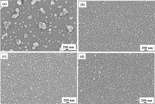
Figure 3. FESEM micrographs of the nanocrystalline NiO films deposited at substrate temperature of: (a) 26 °C, (b) 100 °C, (c) 200 °C and (d) 300 °C.
Download figure:
Standard image High-resolution image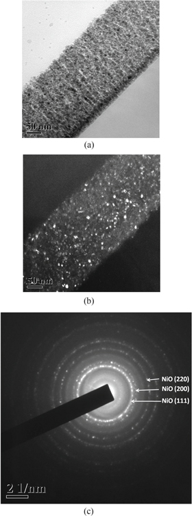
Figure 4. Shows the bright field image (a), dark field image (b) and corresponding SAED pattern (c) for the NiO films deposited at 100 °C.
Download figure:
Standard image High-resolution image3.4. Band gap analysis
The Direct band gap of NiO films deposited on glass substrate at substrate temperature of 26 °C, 100 °C, 200 °C and 300 °C has been measured using absorbance data obtained by UV-visible double photospectrometer in the scan range of 300 nm to 1000 nm. The spectral absorbance data obtained for the investigated NiO films has been plotted against wavelength of incident photon, as shown in figure 5. It shows absorbance is high in ultra-violate (UV) and visible region, and low in infra-red (IR) region. From figure 5 it is also clear that absorbance of NiO films increases towards UV region and decreases towards IR regions and after certain point it becomes constant in IR regions. The absorbance peak shifted towards lower wavelength side in UV region for the NiO films deposited at higher temperatures like 200 °C and 300 °C.
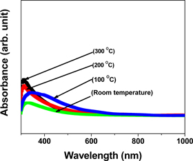
Figure 5. Variation of absorbance with wavelength of incident photon for the nanocrystallineNiO films deposited at different substrate temperature.
Download figure:
Standard image High-resolution imageIn high absorption region, the coefficient of absorption (α) and incident photon energy (hν) is related to the formula written in equation one for the direct transition [36, 37].

Where α = d−1log (1/T), d = film thickness, T = transmittance, h = plank's constant, ν = frequency, Eg = band gap, A = constant
The variation of (αhν)2 with respect to energy of photon for the nanocrystalline NiO films deposited at substrate temperature of room temperature, 100 °C, 200 °C and 300 °C are shown in figure 6. The tangent drawn on the straight portion of the (αhν)2 versus energy of incident photon intercepts the x-axis for the zero absorption which gives the value of direct band gaps. Further obtained value of band gaps have been plotted against grain size of the nanocrystalline NiO films deposited at different substrate temperature is shown in figure 7. It shows decrease in band gap with increase in grain size. The higher value of band gap in the NiO thin films at relatively lower grain size is mainly because of quantum size effect [38]. NiO films with smaller grain sizes have larger grain bounder area which leads to high amount of imperfections causes' larger free charge carrier concentration and high potential barriers which are responsible for the increase in band gap with decrease in grain size. Furthermore decrease in direct band gap for the higher grain size NiO films may be due todecrease in the fraction of grain bounder imperfections and also be involvement of the internal stress developed during the growth of the NiO films.
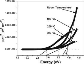
Figure 6. Shows the variation of (αhν)2 with respect to energy of photon for the nanocrystalline NiO films deposited at different substrate temperature.
Download figure:
Standard image High-resolution image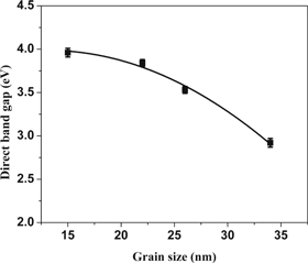
Figure 7. Shows the variation of band gap with grain size of nanocrystalline NiO thin films.
Download figure:
Standard image High-resolution image
4. Conclusions
The NiO thin films have been processed by reactive magnetron sputtering in argon and oxygen gas environment. The GIXRD results show the presence of naocrystalline NiO phases with 〈111〉 orientation as preferred orientation. The GIXRD results also confirm the increase in grain size from 12 nm to 28 nm with increase in deposition temperature from room temperature to 300 °C. FESEM micrographs of NiO thin films reveal the agglomerated surface morphology at room temperature and more uniform distribution of grains over substrate at higher temperature like 200 °C and 300 °C. The analysis of absorption spectra obtained by UV-visible photo spectroscopy show the variation of direct band gap from ≈2.92 eV to ≈3.96 eV. Further direct band gap is correlated with grain size and it is found to decrease with increase in the grain size.
Acknowledgments
Author is thankful to Indian Institute of Technology Kharagpur and Shree Guru Gobind Singh Tricentenary University Gurgaon, Delhi-NCR for their supports.