Abstract
In this paper we demonstrate the ability to fabricate fishnets by nanoimprinting directly into a pre-deposited three layer metal–dielectric–metal stack, enabling us to pattern large areas in two minutes. We have designed and fabricated two different fishnet structures of varying dimensions using this method and measured their resonant wavelengths in the near-infrared at 1.45 μm and 1.88 μm. An important by-product of directly imprinting into the metal–dielectric stack, without separation from the substrate, is the formation of rectangular nanopillars that sit within the rectangular apertures between the fishnet slabs. Simulations complement our measurements and suggest a negative refractive index real part with a magnitude of 1.6. Further simulations suggest that if the fishnet were to be detached from the supporting substrate a refractive index real part of 5 and FOM of 2.74 could be obtained.
Export citation and abstract BibTeX RIS

Content from this work may be used under the terms of the Creative Commons Attribution 3.0 licence. Any further distribution of this work must maintain attribution to the author(s) and the title of the work, journal citation and DOI.
1. Introduction
Since its inception and experimental demonstration [1–3] the fishnet structure has been a staple of metamaterial research, particularly with regard to negative-index metamaterials (NIMs) [4–6]. The capability of the fishnet structure for producing negative (real part) values of permittivity ( ) and permeability (μ) that can be separately tuned by altering the physical dimensions of the structure [7, 8] allows for a negative refractive index at frequencies where both and μ are simultaneously less than zero. The fishnet structure can be physically described as an array of perpendicularly interlocking thin metal wires stacked on top of a dielectric layer that separates the wires from another set of parallel metal wires, as shown in figure 1. This configuration allows the fishnet to be regarded as an effective LC circuit array for theoretical and modelling purposes. Wide metal slabs that partly make up the grid lattice enable the creation of anti-symmetric currents when they are aligned parallel to the direction of the magnetic field of the incident light. These currents in turn create a magnetic response that, near-resonance, can produce negative values for μ. The values produced for are dependent on having metal wires that are narrower than the slabs used to induce a magnetic response and are orientated perpendicularly, on the same plane as the electric field of the incident light. By acting as a diluted metal with a lower plasma frequency, the wires can therefore produce a negative permittivity. This ability to exhibit negative values of and μ allows fishnets to operate as a NIM, a characteristic that has been well reported at near infrared (NIR) and visible wavelengths [9–11].
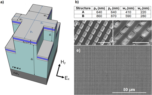
Figure 1. (a) Model of an ideal single unit cell of the fishnet with pillars, detailing dimensions and material thicknesses (not to scale). The depth of the PMMA layer at its thickest, dt, is 1000 nm. This is the thickness of the PMMA when it is spun onto the SiO2 substrate. The fishnet sits on the top of the sample with the pillars pressed down into the PMMA layer. The imprinted depth of the pillars in the PMMA is denoted by di, which equals 300 nm for both designs. The metal–dielectric–metal tri-layer of silver–magnesium fluoride–silver (Ag–MgF2–Ag) is denoted by tm–d–m and has a total thickness of 110 nm (30 nm Ag, 50 nm MgF2, 30 nm Ag). Light incident normally on the top face of the fishnet is polarized as shown inset. (b) Table listing the measured dimensions of the two fabricated structures. (c) An angled micrograph of a silicon carbide (SiC) stamp used for imprinting, showing etched rectangular pillars 1 μm in height. (d) A fabricated fishnet and metal–dielectric–metal pillars, as observed at an angle of 25° with respect to the normal. The dark region that separates the fishnet from the pushed-down pillars is made of PMMA. The scale bar for both (c) and (d) is 3 μm long. (e) A micrograph of the fishnet and pillar structure showing an enlarged area of structure B.
Download figure:
Standard image High-resolution imageCommon fabrication techniques for fishnets involve focused ion beam milling of a pre-deposited material stack [9] or electron beam patterning followed by the deposition of subsequent metal and dielectric layers [11], i.e. a 'lift-off' process. While these methods can undoubtedly produce high quality structures with resolution in the sub-100 nm scale, there are associated disadvantages that stem from them—primarily a limited pattern area, large patterning time and high costs. Furthermore, these techniques can result in structural asymmetry in the form of tapered sidewalls, introducing bianisotropic effects that reduce the effectiveness of the medium as a negative index material. A number of studies have investigated the use of nano-imprint lithography (NIL) as a technique in fabricating fishnet [12–15] and nano-hole arrays [16–19], as well as a variety of metamaterial structures [20, 21]. In addition to this, a range of different nano-imprint processes have been studied [22–24], including direct imprinting [25–28]. In this paper we report our work in fabricating two designs with differing dimensions of three layer (single active layer) fishnet with nanopillars by imprinting directly into a metal–dielectric–metal stack. These designs, detailed in figure 1, are referred to as structure A and structure B throughout this paper. Analysis of the imprint technique and the quality of the fabricated structures is also given.
Additionally we find distinct optical responses at NIR wavelengths for each fishnet design and calculate values for the refractive index and figure of merit (FOM) using finite difference time domain (FDTD) simulations that complement our experimental measurements. Field plots showing the electric and magnetic field strengths in both reflectance and transmission modes have also been obtained from the simulations. We believe that this NIL technique can be adopted to create, easily and rapidly, low-cost, large-area, 3D metamaterial structures.
2. Experiments and simulations
A SiC nanoimprint stamp is fabricated by electron-beam lithography using hydrogen silesquioxane (HSQ) as the resist and, post development, as a mask for inductively coupled plasma etching. The cleaved SiC substrate used was 500 μm thick and measured 1 cm2 in area, with a square patterned area of 3 mm2. After etching to a depth of 1 μm the HSQ is removed by hydrofluoric acid (HF)—after which the sample is treated in a solution of heptane and silane F13-OTCS ((tridecafluoro-1,1,2,2-tetrahydrooctyl)-trichlorosilane), a common hydrophobic non-stick coating for silicon substrates. This treatment prevents the stamp adhering to the target sample during imprinting and eases separation after patterning. It is important to achieve vertical sidewalls following the etch process, in order to avoid distortion of the pattern dimensions in the fabricated structure during the imprinting process. The target sample consists of a polished fused silica substrate that is spin-coated with a 1 μm thick layer of polymethyl methacrylate (PMMA). A metal–dielectric–metal tri-layer of Ag (30 nm), MgF2 (50 nm) and Ag (30 nm) is then electron-beam evaporated on to the PMMA. Silver has been selected in preference to gold because of the lower associated optical losses [3]. The SiC stamp is imprinted directly into the tri-layer using a modified Specac hydraulic press—applying a half tonne force (4.9 kPa pressure) at room temperature. The etched SiC pillars define the structure when imprinted and displace part of the metal–dielectric–metal tri-layer into the PMMA beneath, forming rectangular pillars in the apertures of the fishnet. The PMMA beneath the metal–dielectric stack is compressed when the nanopillars are displaced from the fishnet. The compression of PMMA has been shown to change the associated refractive index [29]. The behaviour of PMMA during the imprinting process has also been reported [30]. From [29] we estimate that with the imprint force used the refractive index real part of the compressed PMMA may increase by approximately 0.05, although it should be noted that the values stated in [29] are given for shorter wavelengths than measured here. This change is noted but the variation of index with pressure is not modelled. The imprinting process itself typically takes only two minutes and the stamp can be cleaned in acetone afterwards for re-use. It was found in our experiments that the stamps can be used at least ten times without damage occurring. While the etched pillars remained intact throughout, continued use of a stamp for more than ten imprints resulted in the gradual formation of small cracks in the SiC. These cracks eventually resulted in fragments breaking from the substrate, usually near the cleaved edges. The depth of the pillars can be varied with the imprint force used, but we have found that a half-tonne force (4.9 kPa pressure) results in a depth in the PMMA of approximately 300 nm from the fishnet on top. The NIL process is often enhanced by reducing the viscosity of the polymer that is to be patterned by heating the substrate [31]. However, we have observed that heating the PMMA to improve its flow causes the metal and dielectric layers on top of the PMMA to crack and break up, making lithography at room temperature desirable. The fabricated fishnet and nano-pillar structure exhibits good uniformity across the patterned 3 mm2 area, with only small, localized regions at the four corners of the imprinted area showing breaks in the metal–dielectric–metal tracks. Close inspection of the imprinted pattern, shown in figure 2, shows uniform, continuous silver wires. The apertures defined by the imprint are consistent in dimension and show rounding at the corners. The edges of the wires exhibit roughness resulting from the cutting of the metal and dielectric by the SiC pillars. Nano-sized cracks are also visible on the imprinted nano-pillars, the regions that are in direct contact with the nanoimprint stamp. Unlike other techniques that utilize NIL to pattern a resist or polymer mask, imprinting directly into the metal–dielectric–metal stack removes the need for etching [12, 13].
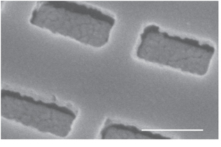
Figure 2. Angled SEM micrograph of structure B showing, in detail, the interlocking Ag–MgF2–Ag wires, and imprinted nano-pillars pushed into PMMA. The dark region located between the fishnet and imprinted nano-pillars is PMMA. The scale bar is 500 nm.
Download figure:
Standard image High-resolution imageReflectance and transmission measurements were obtained using a Bruker Hyperion microscope attached to a vertex Fourier transform infrared spectrometer, configured for NIR wavelengths and using a CaF2 beamsplitter. Reflectance measurements were taken by illuminating the top of the fishnet and measuring the reflected light, while transmission was measured by passing light through the silica substrate and measuring from above the fishnet. The light incident on the sample was polarized as indicated in figure 1 using a ZnSe crystal polarizer. The reflection measurements were normalized using an unpatterned 30 nm thick sheet of silver on a fused silica substrate as a background—and transmission measurements were normalized against a fused silica substrate with 1 μm of PMMA spun on top.
Using the dimensions and constituent material properties of the two different fabricated structures, we have simulated reflection and transmission spectra using the FDTD method to complement the experimental results. The electromagnetic properties of the imprinted fishnet structure were studied by computer simulation using Lumerical FDTD solutions software. The transmission and reflection characteristics were calculated from a single unit-cell and a polarized plane wave source with its polarization defining electric field component, Ex, perpendicular to the long axis of the fishnet slab. The imprinted fishnet stack was illuminated by a plane wave source over the wavelength range from 1000 nm to 4000 nm. The simulation area was a rectangular parallelepiped shape. The calculation region is 660 × 660 × 2000 nm3, with a conformal mesh region self-adapted to the structure. The very fine mesh size of 3 nm was used within the metal layers and was adequate for simulation convergence. For simulations of just the fishnet portion of the structure, the calculation region is set with a background index of air (n = 1). Depending upon the polarization of the source, the periodic boundaries in the x- and y-directions are replaced by imposing an anti-symmetric/symmetric condition. A perfectly matched layer was imposed on the edge planes of the simulation area, perpendicular to the direction of source propagation. The refractive index of the dielectric spacer material, MgF2, was set to 1.38. A Drude model was used for the dielectric function of Ag, with a plasma frequency of 9.0 eV and damping frequency of 0.054 eV [32]. The damping frequency was increased by a factor of three compared with that of bulk silver to account for the additional surface scattering losses in real films [33]. The silica substrate was considered to be semi-infinite in the simulations.
3. Results and discussion
There is close agreement between the experimental and simulated reflection and transmission spectra, shown in figure 3. Resonances are observed experimentally at 1.45 μm and 1.88 μm respectively, as the critical dimensions of the structure are increased in scale. The experimental transmission spectra show a trough at approximately 2.7 μm with near-zero transmission for all three structural dimensions. This trough can reasonably be attributed to the excitation of the O–H ion stretch vibration at 2.7 μm in the fused silica substrate, not the fishnet and pillar structures or the PMMA that supports them. The magnitude of the experimental transmission at negative index wavelengths is, at maximum, approximately 40% and 65%, for structures A and B respectively. Both the experimental and simulated transmission and reflection spectra are absolute and not arbitrary units. It should be noted that the metal–dielectric–metal pillars that are depressed into the PMMA fill the areas beneath the apertures of the fishnet, meaning that transmitted light must pass through the sidewall of the rectangular PMMA holes, as well as by extraordinary transmission through the sub-wavelength hole array [34, 35]. The divergence between experimental and simulated results below 1.5 μm can be attributed to Fabry–Perot resonances between the fishnet, nanopillars and substrate which are accentuated in the simulations due to impedance mismatch and seen in other reported work concerning fishnets [9].

Figure 3. Measured and simulated transmission and reflectance spectra of fishnets and nanopillars of varying dimensions, with a micrograph of each structure inset. The scale bar is 2 μm in both instances. The spectra are obtained from structures patterned to the specifications detailed in figure 1: (a) structure A, (b) structure B. The shaded regions on both plots indicate the wavelengths at which n is negative.
Download figure:
Standard image High-resolution imageFrom the simulated spectra we can retrieve the wavelength-dependent refractive index and FOM values [36] of the fabricated structure, shown in figure 4. The FOM is defined by the ratio of Re(n)/Im(n), where Re(n) is the refractive index real part and Im(n) is the imaginary part.
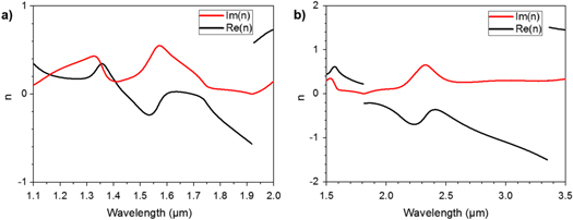
Figure 4. Real and imaginary values of n obtained from simulations modelling the fishnet and pillars structure supported on PMMA for the dimensions of (a) structure A and (b) structure B. The discontinuities observed are, taking scaling of dimensions into consideration, consistent with those previously reported by Koschny et al [40] and Zhou et al [44].
Download figure:
Standard image High-resolution imageThe modified retrieval method for asymmetric structures has been used to retrieve the complex effective index of the structure [37–40]. It should be noted that the retrieval process is not, in general, trivial—especially when the metamaterials of interest are anisotropic or bianisotropic [41, 42]. If the optical path length across the unit cell of a structure is not small, then the effective medium limit even for a symmetric structure is not applicable. If the unit cell is not symmetric in the direction of propagation then the standard retrieval procedure fails to provide a unique answer for n [40]. To calculate the generalized scattering parameters; we consider the two values of the reflection coefficient when illuminating from free space (S11) or through the substrate (S22). The differences between the magnitudes of S11 and S22 are modest. However there is a large contrast in the phases of S11 and S22, implying very different properties for the structure and depending on which side of the unit cell is first impacted by the incoming wave (both the phases and magnitudes of S12 and S21 are identical) [36].
The fishnet and nanopillars of structures A and B on a 1 μm thick layer of PMMA and silica substrate were simulated to show the real and imaginary part of the refractive index near the respective resonant wavelength and are shown in figure 4. For structure A, a refractive index real part of −0.24 was found at 1.53 μm. This decreased to a maximum magnitude of −0.57 at 1.9 μm. With structure B a refractive index of −0.7 was observed at 2.35 μm and was shown to decrease to −1.5 at 3.35 μm. The PMMA and suppressed pillars are here responsible for the increasing material losses and for limiting the magnitude of n. The broad response of Re(n) in figure 4 is consistent with previously reported periodicity effects in metamaterials with reduced symmetry [40]. The FOM for the as fabricated structure is not presented because discontinuities due to multiple refractive changes in the material make the calculation unreliable. It should be remembered that any optimization of the pillar dimensions [43] using the NIL technique that we have described will also alter the dimensions of the fishnet, since both are defined by the same nanoimprint stamp.
The calculation of such a negative refractive index and FOM, coupled to the ease with which the structures can be fabricated by NIL, increases the desirability of detaching the fishnet for transfer to an alternative substrate or, indeed, for suspension in air. While we have not detached the fishnet from the PMMA, depositing a sacrificial soluble layer or imprinting onto PDMS remain plausible methods for achieving pattern transfer. Simulated field plots, displayed in figure 5, show the electric field distribution through a single unit cell of the fishnet as well as interaction between the fishnet and the pillars imprinted in PMMA beneath. All the plots are calculated at the wavelength of magnetic resonance, 1.45 μm or 1.88 μm for structures A and B respectively.

Figure 5. Field plots showing the electric field across two different planes of the structures, with incident light polarized as indicated in figure 1. An outline of the structure has been added for clarity. Axis values are in microns and indicate the dimensions of each structure. (a) Electric field distribution of a single unit cell of structure B at resonant wavelength 1.88 μm, showing the top silver layer of the fishnet and aperture on the x-y plane. (b) A cross section of structure A (y-z plane) showing the electric field distribution of the Ag–MgF2–Ag in the fishnet, pillars and supporting PMMA at a wavelength of 1.44 μm. (c) The y-z plane cross section field plot of structure B at a wavelength of 1.88 μm.
Download figure:
Standard image High-resolution imageFigure 5(a) shows a unit cell of the fishnet and nanopillar on the x-y plane from normal incidence. The wide metal tracks exhibit a strong electric field induced by the magnetic field of the incident wave. This field distribution does not correspond to Bragg scattered surface waves. The field plots in figures 5(b) and (c) show electromagnetic coupling between the fishnets and pillars, through the PMMA. As a means to gauge the effect of the PMMA, nanopillars and silica substrate, simulations modelling only the fishnet portion of structure A and B were also performed and are shown in figure 6. The simulation that modelled solely the fishnet for structure A (and not the nanopillars on PMMA) shows a refractive index of −4 and a FOM of 2.49, while the equivalent values for structure B are −5 and 2.74 respectively. These values are comparable with those quoted for single active layer fishnets that have been reported previously [9, 10, 15].

Figure 6. Simulated n and FOM values plotted against wavelength for the fishnets only, without the PMMA, metal–dielectric–metal pillars or quartz substrate. Values are obtained using dimensions measured from the fabricated fishnets and with the structure suspended in air. (a) Real and imaginary parts of the refractive index obtained for structure A, (b) the FOM calculated for the same structure, (c) refractive index values obtained for structure B and (d) the FOM for structure B. The fishnet from structure A has a negative refractive index of magnitude 4 at 1.48 μm. The structure B fishnet exhibits an n value of −5 at 2.09 μm. The maximum FOM is calculated as 2.49 and 2.74 for the fishnets of structure A and structure B respectively.
Download figure:
Standard image High-resolution image
The results shown in figure 6 suggest that if the fishnet were to be detached from the supporting PMMA and substrate, the negative real part of the refractive index would increase in magnitude, making a more effective metamaterial.
4. Conclusions
We have demonstrated a rapid and effective method for fabricating negative index fishnets. Unlike conventional fishnet fabrication techniques based on direct-write electron-beam lithography, imprinting directly into a metal–dielectric–metal film stack does not require an etch process and enables large-area patterns to be produced. The structural quality and uniformity of the fishnets is good, with some roughness noted at the edges of the apertures. We also note that damage, in the form of cracking, is inflicted on the regions of metal directly in contact with the nanoimprint stamp. Simulations have shown that the refractive index and FOM values of our fishnets are comparable with those previously reported from single active layer fishnets. We believe that the NIL technique presented in this paper can be adapted for use in pattern transfer, by lifting the imprinted fishnet from a sacrificial layer and moving it to a new substrate, such as PDMS. Imprinting into a greater number of metal–dielectric multi-layers, so as to increase the magnitude of the negative refractive index, also remains feasible.
Acknowledgments
The authors would like to acknowledge the facilities and staff of the James Watt Nanofabrication Centre at the University of Glasgow where the structures reported in this paper were fabricated. We also acknowledge support from the EPSRC in the form of a scholarship for Graham J Sharp (grant number EP/J500434/1).