
Abstract
Graphene is hailed as an ideal material for spintronics due to weak intrinsic spin–orbit interaction that facilitates lateral spin transport and tunability of its electronic properties, including a possibility to induce magnetism in graphene. Another promising application of graphene is related to its use as a spacer separating ferromagnetic metals (FMs) in vertical magnetoresistive devices, the most prominent class of spintronic devices widely used as magnetic sensors. In particular, few-layer graphene was predicted to act as a perfect spin filter. Here we show that the role of graphene in such devices (at least in the absence of epitaxial alignment between graphene and the FMs) is different and determined by proximity-induced spin splitting and charge transfer with adjacent ferromagnetic metals, making graphene a weak FM electrode rather than a spin filter. To this end, we report observations of magnetoresistance (MR) in vertical Co-graphene-NiFe junctions with 1–4 graphene layers separating the ferromagnets, and demonstrate that the dependence of the MR sign on the number of layers and its inversion at relatively small bias voltages is consistent with spin transport between weakly doped and differently spin-polarized layers of graphene. The proposed interpretation is supported by the observation of an MR sign reversal in biased Co-graphene-hBN-NiFe devices and by comprehensive structural characterization. Our results suggest a new architecture for vertical devices with electrically controlled MR.
Export citation and abstract BibTeX RIS

Original content from this work may be used under the terms of the Creative Commons Attribution 3.0 licence. Any further distribution of this work must maintain attribution to the author(s) and the title of the work, journal citation and DOI.
Following the successful development of graphene-based lateral spintronic devices [1–3] and the demonstration of intrinsic [4] and proximity-induced [5–9] magnetism in graphene, the implementation of graphene as a spacer in vertical magnetic tunnel junctions (MTJ) has become a subject of intense interest [10–20]. Up to now, theoretical proposals [10–12] for graphene's role in MTJs focused on the so-called 'K-point spin filtering' expected in ideally lattice-matched single-crystalline ferromagnet–graphene–ferromagnet (FM–G–FM) structures and attributed to matching spin-polarized bands in the ferromagnet and the electronic states in the graphene treated as a tunnelling barrier. This mechanism was also used to interpret the MR sign inversion observed in conventional Ni–Al2O3–Co [13] and Ni–MgO–Co [14] tunnel junctions where the Ni electrode was passivated by CVD grown (epitaxial) mono- [13] or few-layer [14] graphene. However, despite several attempts, no significant spin filtering could so far be achieved in vertical magnetoresistive devices where graphene was used as a spacer between two FM electrodes without an additional insulating barrier [15–20], in contrast to theory predictions [10–12]. The most likely reason for this is that the reported FM–G–FM sandwiches (especially those fabricated by a combination of graphene transfer and deposition of FM films) were in fact van der Waals heterostructures [21, 22] rather than truly lattice-matched crystals. In this case, as we show below, graphene plays a different role, itself becoming a source of spin-polarized electrons due to the interplay of (i) its doping by charge transfer from the FM metal and (ii) proximity-induced spin splitting in graphene.
To explore such a possibility, one needs to create contamination- and oxidation-free G–FM interfaces, but without the requirement of lattice matching between G and the FMs. To this end, we have fabricated vertical FM–G–FM' devices where ultimately clean G–FM interfaces were obtained by depositing the ferromagnetic metals on the two sides of a suspended graphene membrane, thereby preventing oxidation, minimizing the number of fabrication steps and limiting the exposure of the devices to solvents during preparation (here FM = Co and FM' = Ni0.8Fe0.2 alloy). Details of sample fabrication and characterization are given in methods and supplementary figures S1–S3 and S8 (stacks.iop.org/TDM/4/031004/mmedia). Briefly, an exfoliated graphene (or hBN) flake was suspended over a 3–4 µm diameter circular aperture in a 100 nm-thick SiNx membrane using a dry transfer method [23]. The FM electrodes were then evaporated onto the suspended flake from the top and bottom side as shown schematically in figure 1(a) and supplementary figure S1 (a similar approach was used in [15], but our method is different in several important aspects, as described in methods and supplementary note 1). After the first (top) deposition, the metal at the interface was protected from oxidation by graphene, as the latter is known to act as an impermeable barrier for all gases and liquids [13, 24], which also implies that pinholes are virtually non-existent.
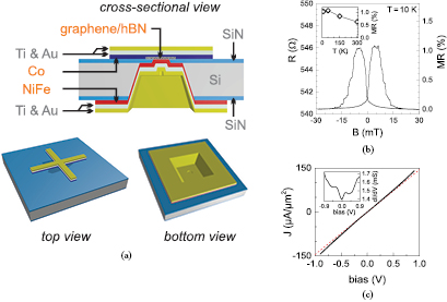
Figure 1. Sample design and magnetoresistance of the reference Co-hBN-Py device. (a) Design of the samples. Ferromagnetic Co and Ni0.8Fe0.2 films (each 20 nm thick) were deposited on the top and bottom side, respectively, of graphene (or hBN) suspended over a 3.5 µm diameter aperture in a 100 nm thick SiNx window. On the top side, a Greek cross geometry was used. On the bottom side, a larger square area was covered by the NiFe–Ti–Au film. (b) Resistance R of the hBN-based device versus the applied in-plane magnetic field B (T = 10 K); MR ≈ 1%. Shown behavior is typical for all T up to 300 K. Inset: temperature dependence of the MR (◊). The line is a guide to the eye. (c) Main panel: current–voltage characteristic of the hBN-based device at T = 10 K (black solid line). Its tangent line at zero bias (red dashed line) is shown to illustrate a slight bending of the curve for higher bias, indicative of tunneling behavior. The inset shows the corresponding dI/dV curve.
Download figure:
Standard image High-resolution imageTo test our fabrication procedure, we first made a device where Co and Ni0.8Fe0.2 (Py) electrodes were separated by bilayer hexagonal boron nitride (hBN) instead of graphene. Atomically thin hBN has been shown to act as a high-quality insulating barrier in vertical transistors [25], lateral spin valves [26] and, most recently, in magnetic tunnel junctions (MTJs) [27]. Figures 1(b) and (c) show magneto-transport characteristics of our FM–hBN–FM' device. These are consistent with classical MTJ behavior: The two electrodes are magnetically separated and switch independently, with a TMR value of ≈1% at a temperature T = 10 K. Using Jullière's formula [28]  and a simplifying assumption
  (equal spin polarization for both FM electrodes) we obtain an average spin polarization of the ferromagnets P ~ 7%. These characteristics compare very favorably with P ~ 0.05–0.25% and TMR ~ 0.3–0.5% reported for Co-hBN-NiFe MTJs based on hBN grown by chemical vapor deposition (CVD) and transferred onto the FM [29] and are of the same order as the more recent work [27] where the hBN barrier in Fe/hBN/Co MTJs was grown directly on Fe. The temperature-dependent MR shown in the inset of figure 1(b) is also in agreement with the usual TMR behavior [28–31]: the MR decreases by 40% as the temperature is increased from 5 K to 300 K, which is commonly attributed to magnon excitations [30, 31]. Furthermore, the non-linear I(V) characteristics (figure 1(c)) and the resistance × area (RA) product of 6.2 kΩ · µm2 at 10 K agree with previous measurements on a 2-layer hBN tunnel barrier [32] and the corresponding dI/dV (inset in figure 1(c)) is in agreement with earlier studies of Co-based MTJs with AlOx barriers [33]. Finally, we have checked that our fabrication method does not lead to unintentional contacts between the top and bottom FM films by preparing several test samples without the graphene-covered aperture and found resistances >10 MΩ, confirming that the current flows through the junction area only.
Having proven the technology, we fabricated a set of ten Co-G-Py structures, where FM electrodes are separated by mono-, bi-, tri- or four-layer graphene, and studied their vertical magnetoresistance. The sample design is shown in figure 1(a). Typical variations of the magnetoresistance as a function of in-plane magnetic field, B, at different temperatures, T, are shown in the top row of figure 2(a) and supplementary figure S5. Similar to the hBN-based MTJ device, all graphene-based junctions showed positive MR, with plateau regions in the R(B) traces, as expected in a regular MTJ device, indicating that already a monolayer of graphene is sufficient to decouple the switching of the two FMs. This is consistent with earlier reports, where a similar decoupling of the ferromagnetic electrodes has been observed for a monolayer graphene spacer [15, 16]. At the same time, the resistance of all devices was quite low (between 2 and 20 Ω) and I(V) characteristics were linear (supplementary figure S4), corresponding to metallic behavior. This is in stark contrast to some previous reports [15–17] where graphene-based structures showed tunneling behavior; e.g. [17] reported junction RA products in excess of 35 kΩ · µm2, probably due to partial oxidation or residual contamination of the ferromagnetic films during the transfer of graphene in ambient conditions. Concerning the origin of MR in our devices, we used angle-dependent measurements to verify that it was not due to anisotropic magnetoresistance (see supplementary note 3 for details).

Figure 2. Magnetoresistance of graphene-based vertical junctions (Co-G-Py) as a function of the number of layers. (a) Low-temperature MR traces for mono-, bi- and trilayer graphene devices before and after annealing (top and bottom panels, respectively). For N = 2 and 3, MR changes sign, which is accompanied by an increase in coercivity of the Co electrode. (b) Temperature-dependent MR of mono-, bi- and trilayer graphene devices before (□,  ,
,  ) and after (
 ,
,  ,
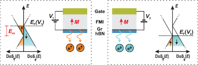
,  ) annealing. Arrows indicate the change in MR after annealing. (c) Schematic spin-dependent density of states, DoS↑/↓(E), for the constituent layers of a device with N ⩾ 2 (see text). The Fermi levels of graphene layers adjacent to the FMs are shifted due to n-doping and p-doping from Co and Py, respectively. Proximity-induced exchange splitting results in different DoSs for graphene's spin-up and spin-down carriers at EF. The thick dashed line in the middle indicates decoupling of the van der Waals bonded graphene layers as they conform to the FM films (see text).
Download figure:
Standard image High-resolution imageIn terms of RA and MR values, there was no correlation between the number of graphene layers, N, separating the FM electrodes and the device behavior (top row of figure 2(a), figure 3(a) and supplementary figure S5), despite the identical fabrication conditions. For example, for three N = 2 devices the measured RA products were 17, 29 and 309 Ω · µm2, with MR = 1.03%, 0.66% and 0.10%; for two N = 4 devices these were 38 and 136 Ω · µm2, or 0.42% and 0.12%, respectively. A similarly large spread of characteristics was found for N = 3 (RA = 23, 170, 193 Ω · µm2 with MR = 0.9%, 0.30%, 0.12%) and N = 1 (RA = 110, 175 Ω · µm2 with MR = 0.09%, 0.2%) junctions. The contribution from the resistance of gold leads, ~1 Ω, could only play a role for two devices with the smallest R (see above). Furthermore, the large average value of RA across all samples, 120 Ω · µm2 (much higher than for a typical metal) and the almost temperature-independent RA for most devices, including an increasing RA at low T for N = 3 and 4 in figure 3(a), are strong indications that the measured R of the devices is determined by the resistance of G–FM interfaces and not the metallic leads [34].
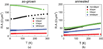
Figure 3. Temperature dependence of the RA product before and after annealing for Co-G-Py junctions. (a) Temperature dependences of the RA product for N = 1 ( ), N = 2 (
 ), N = 3 (
 ) and N = 4 (
 ) graphene devices before annealing. No correlation can be discerned between N and the device resistance and neither of the samples shows a metal-like RA(T) dependence. (b) Temperature dependences of the RA product for the same devices after annealing. All devices show metal-like behavior, with a significant reduction in RA values compared to their as-grown state. The rather large statistical spread of data narrows down after annealing (we attribute the RA distribution before annealing to the presence of numerous voids at the interface, see text).
Download figure:
Standard image High-resolution imageThe surprisingly wide spread of (magneto) transport characteristics of our devices and the apparent lack of dependence on N can be understood if we recall that the deposition of relatively thick, ~150 nm, metallic films on suspended, atomically thin graphene membranes is likely to result in significant strains in the devices, evident from their topography at different stages of preparation, e.g. the 'Mexican hat' shape shown in supplementary figure S2. Strains will inevitably affect, locally, the atomic-scale separation between the FM and the adjacent graphene layer. To relieve such strains and further improve the interface quality, we annealed several representative devices with different N at 300 °C in Ar/H2 atmosphere for up to 10 h. Annealing under such conditions is known to significantly improve the interfaces in van der Waals heterostructures [23, 35], and for our devices was confirmed by cross-sectional transmission electron microscopy (see below). This resulted in a strong change in both RA and MR, leading to a consistent behavior of all devices—see figures 3(a) and (b). The RA of all samples dropped significantly after annealing, from 17–196 Ω · µm2 to 8–51 Ω · µm2 at 10 K, and its temperature dependence became metal-like for all devices, unlike the almost flat or slightly increasing RA at low T for the as-prepared samples. The change in magnetoresistance was even more dramatic: For devices with N = 2 and 3 MR changed sign and in some cases increased in absolute value (e.g. for N = 3 at T = 10 K from +0.30% before annealing to −0.6% after), see figures 2(a) and (b). For N = 4 it dropped from MR = 0.4% to almost zero (supplementary figure S6). Only for the monolayer device, N = 1, MR remained small and positive, slightly increasing from 0.1% to 0.14%.
Another change in device behavior becomes clear from comparison of the coercivities of the FM layers before and after annealing (figure 2(a)): these increased significantly, especially for N = 2 and N = 3, indicating more uniform magnetization in our polycrystalline FM films. It is therefore natural to attribute the increase in coercivity to relaxation of stresses both in the FMs and at the interface between a FM and the adjacent graphene layer. We note that the annealing temperature was too low to expect any significant recrystallization [36] and, indeed, no noticeable changes in grain sizes could be seen when the FM films were observed through transparent graphene in a scanning electron microscope (SEM), see supplementary figure S3. Nevertheless, SEM observations of test samples (only one FM deposited on graphene, before and after annealing) did show signs of rearrangements of the individual crystallites in our polycrystalline FM films after annealing (supplementary figure S3), which can be attributed to strain relaxation [36]. Relaxation of strains was also evident from atomic force microscopy (AFM) imaging of the junctions' topography after annealing (typical example is shown in supplementary figure S2): The 'Mexican hat' shape is no longer present (unsurprisingly, some sagging of the suspended area remains).
To confirm that the implied structural changes at the graphene-FM interfaces indeed take place in our Co-G-Py junctions, two representative devices before and after annealing were examined using cross-sectional transmission electron microscopy (TEM)—see supplementary figure S8 and the associated discussion. This revealed the presence of significant, several nm-wide, voids between graphene and the ferromagnetic films before annealing, consistent with the observed large variations in resistance (a few voids are indicated by arrows in supplementary figure S8). The voids effectively determine the MR before annealing, leading to a situation where the interface acts more like a 'bad' tunnel barrier (even though the details of the interface are device specific in this case). After annealing the voids disappeared, resulting in much smoother interfaces and uniform contact between graphene and the FMs, again consistent with the changes in junction resistance. Importantly, the annealing did not affect the chemical composition of the devices, that is, all constituent layers (Au, Ti, Co, Py) remained well defined, with no signs of interdiffusion (supplementary figure 8).
Just an improved contact between graphene and FMs cannot account for the main feature in the behavior of our devices: the sign change of MR after annealing. The widely discussed 'K-point spin filtering', suggested by theory for both graphene-FM and hBN-FM epitaxial interfaces [10–12] and used to interpret a number of experimental findings [13, 14, 16, 20], cannot explain the sign change of MR in our case and, more importantly, is not applicable to our devices. Firstly, the polycrystalline nature of our FM films and the corresponding lack of epitaxy with graphene (or hBN) are contrary to the theory assumptions. Secondly, the RA product in our experiments is 5 orders of magnitude greater than the theoretical value, <0.003 Ω µm2, obtained for 'K-point spin filtering' and attributed to hybridization and covalent bonding [11]. Therefore, we draw attention to two features specific to the FM/graphene interface which have not been considered previously in the context of MTJs: doping due to contact with a metal [37, 38] and exchange splitting due to proximity to a ferromagnet that gives rise to a difference in the density of states (DoS) between spin-up and spin-down carriers in graphene [5–9]. Triggered by annealing, the conformation and improved contact between a FM electrode and the adjacent graphene layer result in effective decoupling of graphene layers within a van der Waals-bonded few-layer crystal, as was seen e.g. for twisted graphene bilayers under annealing [39, 40], producing two electronically decoupled thinner 'graphenes'. Subsequently, these two separately doped and exchange proximitised graphene layers become spin-polarised electrodes defining the device behavior, with a relatively small value of MR but qualitatively new features.
Here, we emphasize an important difference between the studied van der Waals structures and epitaxial G–FM or FM–G–FM' heterostructures. In vdW structures, the absence of lattice matching between the FMs and the adjacent graphene layers prohibits hybridization of the electronic bands of graphene and Co/Py (hybridization would effectively extinguish the Dirac spectrum of graphene). There is consensus between theoretical studies [10, 12, 38] that whether or not hybridization occurs depends strongly on two related factors, lattice matching and the distance, dFM/G, between the metal and carbon atoms. Hybridization is likely to occur for dFM/G ~ 2 Å in lattice-matched structures, such as epitaxial G–Co films [41], or epitaxial G–Ir intercalated by Co [42]). For example, a recent STM and ARPES study of graphene in direct contact with Ni [43] emphasized that precise lattice matching is needed for a shorter dFM/G and hybridization. In contrast, for typical vdW spacings (dFM/G ⩾ 3 Å) graphene's linear spectrum is preserved and proximity-induced spin splitting is expected in the same way as when graphene is in contact with a ferromagnetic insulator [5–9]. In our devices, we were able to measure the graphene/metal distance, dFM/G, directly using cross-sectional TEM (supplementary figure S8). This showed that for the Co-graphene interface (after annealing) dFM/G = 0.39 ± 0.06 nm and for Py-graphene dFM/G = 0.34 nm ± 0.09 nm, see supplementary note 4. The absence of hybridization also prevents direct RKKY coupling of the ferromagnetic electrodes via graphene considered in [41, 42]. In our vdW structures, the distance between two ferromagnetic layers, ~7.4 Å is almost twice longer than in epitaxial structures [41, 42], therefore, the interlayer RKKY interaction in our devices can be neglected, in agreement with the observed independent switching of the polarization of the two ferromagnetic films in our Co-G-Py devices.
In this situation, unique to graphene, the sign of the spin polarization (majority/minority carriers) should depend on the sign and level of doping (even for the same exchange splitting). This is because for spin-split bands in gapless graphene the type (p- or n-) of doping would determine which spin components (up- or down-) would have larger DoS at the Fermi level, as illustrated schematically in figure 2(c). To evaluate the doping in our devices, we prepared test samples as described in supplementary note 5 and measured gate-dependent charge transport in the vicinity of Co and Py contacts. This showed that graphene in contact with Co is n-doped and graphene in contact with Py is p-doped, with corresponding shifts of the Fermi energy, EF, from the charge neutrality point ≈ +100 meV and -190 meV, respectively (supplementary note 5). A scenario corresponding to such doping is illustrated in figure 2(c) for the charge transfer and proximitised exchange splitting generated by the spin-dependent DoS of Co, Py (drawn schematically with partly occupied 3d and 4s states) and the few-layer graphene spacer. In this simple picture, at EF spin-up electrons represent the majority in n-doped graphene and spin-down electrons are the majority in p-doped graphene. It follows directly that the sign of MR will be negative.
Note that the proposed interpretation also explains why, upon annealing, MR increases (slightly) for N = 1 but decreases and changes sign for N ⩾ 2. A monolayer graphene can conform only to one of the FM layers and the small increase in MR can be explained by an improved contact on one side, while few-layer graphene crystals 'split' and electronically decouple, as described above, and become differently polarized, resulting in a negative MR. The sign change for devices with N = 2 and 3 is very clear and occurred in all studied devices. As for the devices with N = 4, they showed a drop in resistance after annealing, consistent with the behavior for N = 1–3, but the sign reversal of MR was not observed (supplementary figure S6). There are at least two likely reasons for the observed difference between devices with N = 2, 3 and N = 4, as explained in detail in supplementary note 3. Briefly, N = 4 graphene is stiffer and one can expect a less effective conformation at the interfaces with the FM films [45]. Also, in the likely event that a tetralayer 'separates' into two bilayers, a smaller metal-induced shift of the Fermi level, EF, compared to the bi- or trilayer devices should result in smaller spin polarizations, very small MR and the absence of (or an incomplete) MR sign reversal, in agreement with our observations.
To further verify the proposed model, we performed additional experiments on Co-G-NiFe and Co-G-hBN-NiFe devices using bias spectroscopy. First, we investigated the bias dependence of MR in Co-G-NiFe devices (with N = 2 and 3) both before and after annealing (figure 4). In contrast to standard MTJs, the role of increasing bias, Vb, in our devices is not only to shift the chemical potentials on the two sides of the barrier but also to change graphene doping (as shown schematically in figure 4), like in a graphene-based vertical transistor [25]. Due to low carrier density in graphene, it is possible to change its doping substantially using bias voltage [25, 46], and even reverse its sign (e.g. from n-doping to p-doping), leading to a change of sign of MR. This is exactly what we observe in our devices, exemplified by the measurements shown in figure 4 for a Co-G-Py junction with a trilayer graphene spacer. We observed a change of MR sign from negative to positive for Vb > +120 mV (electrons flow from Py to Co), and a notable asymmetry in the rate of MR decrease for positive and negative Vb. For negative Vb we only observe a monotonic decrease of MR with increasing bias, as is common in standard MTJs [31, 49]. For positive Vb this usual behavior is outweighed by the changing spin polarization and the reversal of MR sign. Note that, in contrast, a change of the Fermi level in the Co electrode itself which could lead to an MR sign reversal, would require Vb ~ 800 meV, as shown for Co/SrTiO3/La0.7Sr0.3MnO3 MTJs [47]. In our case we were able to tune the MR using much smaller bias voltages: from MR = −0.6% at Vb = 0 to +0.2% at Vb = +230 mV, with the sign change at Vb ≈ +120 mV.
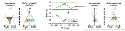
Figure 4. Bias dependence of the magnetoresistance before and after annealing for Co-G-Py devices. Central panel: experimental dependence of MR on the bias voltage, Vb, for a trilayer graphene device before ( ) and after (•) annealing. For the annealed device, MR changes sign from negative to positive at Vb ≈ +120 mV (corresponding to carriers flowing from Py to Co). Right panel: schematic DoS in the two doped and proximitised graphene 'electrodes' at maximum positive Vb (see text). As EF of graphene adjacent to Co shifts into the valence band at Vb > +120 mV, spin-down carriers have a higher DoS in both graphene 'electrodes' and MR becomes positive (see figure 2(c)). Left panel: Schematic DoS in the two graphene 'electrodes' at maximum negative Vb. No sign change of MR is expected, in agreement with experiment, as negative Vb does not change the prevalent spin type at EF for the two graphene electrodes.
Download figure:
Standard image High-resolution imageThe bias dependence of Co-G-hBN-Py junctions (figure 5 and supplementary figure S7) is even more straightforward to understand and is in full agreement with MR(Vb) for our few-layer graphene devices. The MR at zero bias is positive and remains positive after annealing. This implies that the spin polarization in Co-proximitized, n-doped graphene is the same as at the Co-hBN interface [49] (see the positive MR in figure 1 for the Co-hBN-Py device). As the bias is increased to positive values (driving spin-polarized electrons from Py to Co) the Fermi level in graphene is first shifted towards the neutrality point and then into the valence band. Accordingly, the MR decreases and becomes negative (changes sign), on average, at Vb ≈ 80 mV (for the device shown in figure 5 the sign change occurs at Vb ≈ +60 mV while for the other two Co-G-hBN-Py devices, see supplementary figure S7, the MR changes sign at Vb ≈ +80 and +105 mV). We note that a qualitatively similar result (but negative MR) was recently reported for NiFe-G-hBN-Co MTJs [48], although the reason for the suggested negative spin polarization at the NiFe-graphene interface was not identified. An explanation follows directly from our experiments as being due to p-doping of graphene by NiFe.
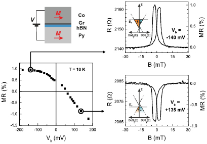
Figure 5. Sign reversal of MR under bias voltage for Co-G-hBN-Py devices. Bottom-left panel: MR as a function of bias voltage, Vb, for a Co-G-hBN-Py device with the spacer between Co and Py made of a monolayer graphene and a bilayer hBN (sketch of the device is shown on the top-left). The panels on the right show magnetoresistance traces for maximum positive and negative Vb, as indicated. The MR sign reversal occurs at Vb ≈ +60 meV, corresponding to a shift in graphene's Fermi energy from the conduction to valence band for increasing Vb (supplementary note 6). The MR was acquired using DC electrical characterization.
Download figure:
Standard image High-resolution imageThe bias values corresponding to the change of MR sign in figures 4 and 5 are remarkably similar to the doping-induced shift of EF in the graphene layer adjacent to Co, ≈ +100 meV, as measured in our separate experiment (supplementary note 5). At first sight this is surprising, as one can expect a certain electrostatic 'back-screening' due to the presence of the second metal layer (Py) close by. To clarify whether such 'back-screening' indeed plays a role, we performed detailed analysis of charge transfer in metal-graphene multilayers (supplementary note 6). This showed that, while the shifts of EF in graphene layers adjacent to Co and Py were smaller than measured in our gate-dependent charge transport experiments (supplementary note 5), for the parameters corresponding to our devices, the bias-induced change of doping polarity in graphene adjacent to Co (from n- to p-doping) occurred at Vb ~ +50 to +100 mV, in excellent agreement with experiment.
Note that the larger value of MR for Co-G-hBN-Py devices compared to Co-G(N = 1)-Py (figures 5 and 2(b), respectively) can be explained by two factors. Firstly, a significant contribution in this case comes from spin polarization at the hBN/NiFe interface, which from our experiments on Co-hBN-Py devices is estimated as ~7%. Secondly, and likely more importantly, the doping level of monolayer graphene in this case is well defined (n-doping) and an appreciable spin polarization can be expected. In contrast, in Co-(N = 1)G-Py devices, doping of graphene is likely to be weak and poorly defined as graphene is in proximity to both Co and Py that dope in opposite sense. This explains that the maximum MR in the latter case is just 0.14%.
Our simple model allows us to estimate the value of the exchange splitting, Eex, in graphene under the simplifying assumption that Eex is the same for Co- and NiFe-proximitised graphene. The MR and the spin polarizations are related through Jullière's formula [28]  , where
  is the spin polarization in Co- or NiFe-proximitised graphene. The spin polarization in graphene, P, is related to Eex by
Here the DoS for spin-up and spin-down electrons are  [44] and the corresponding Fermi energies
  , where
  is the Fermi energy of the (non-exchange split) doped graphene. This means that as the Fermi energy,
  , is shifted further away from the Dirac point by doping or gating, the magnitude of P decreases. In our case, for a doping-induced EF ≈ −150 meV for Py and EF ≈ +30 meV for Co (taking into account finite 'back screening' in FM–G–G–FM sandwiches, as determined in our electrostatics modelling, supplementary note 6), we can assume |PCo| ≈ |5PPy|. With the experimentally obtained |MR| ≈ 0.5% at zero bias (after annealing), we then obtain PCo ≈ 10% and an estimated exchange splitting
  meV. This is a similar order of magnitude as the experimentally measured value of 2 meV for graphene on EuS [8], although larger than 25 µeV found for graphene on YIG in [6] (here we refer to the exchange energy g · µB × |Bexch| [6] resulting from the reported exchange fields Bexch ~ 0.2 T and 14 T for graphene on YIG [6] and EuS [8], respectively).
In conclusion, our results reveal a new role played by graphene in MTJs. In place of the earlier discussed 'K-point spin filtering' suggested for both FM–graphene–FM and FM-hBN-FM epitaxial-quality interfaces [10–12], we find that the major role is played by a combined effect of metal-induced doping and exchange-proximity induced spin polarization in graphene, making it a tunable source of spin-polarised electrons rather than a tunneling barrier. This conclusion opens up a new way to create devices where magnetoresistance can be controlled by the size and polarity of charge transfer in proximitised graphene. More ambitiously, one may achieve electrostatic control over MR by implementing G-hBN-G in van der Waals heterostructures with ferromagnetic insulators, if a larger exchange splitting in graphene is obtained as predicted by theory [7]. At optimal electrostatically controlled doping, this can drive proximitised graphene into the half-metallic state as illustrated in figure 6, offering exciting prospects for graphene applications in MR devices.
Figure 6. Interplay between proximity-induced exchange splitting and charge transfer in MTJs. Shown is a sketch of the optimal conditions for creating fully spin-polarised injectors controlled by electrostatic doping of graphene in proximity to a ferromagnetic insulator. Gate voltages V1 and V2 provide the condition EF± =  µB × |Bexch| for the half-metallic regime in graphene.
Download figure:
Standard image High-resolution image
Methods
All devices were made using a 4-step fabrication process shown schematically in supplementary figure S1. To produce an aperture in the double-sided SiNx(100 nm)/Si(200 µm)/SiNx(100 nm) wafer used as support for FM-G(hBN)-FM' structures, we first used plasma etching (Oxford PlasmaLab System 100 ICP) with a Shipley 1813 photoresist etch mask to remove a ~300 × 300 µm area of SiNx. This was followed by wet etching of the exposed Si in a KOH solution (30 wt.% in H2O at 90 °C) until a 100 nm thick SiNx window was produced, with a typical area ~25 µm × 25 µm. After that a 3.5 µm diameter circular aperture was drilled in the SiNx window using a dual-beam FEI Nova NanoLab 600 focused ion beam (FIB) with 30 kV Ga+ ions at a current of 0.1 nA (prior alignment was done with the SEM column to minimize damage). By approaching the SiNx membrane from the bottom side (supplementary figure S1) FIB etching produced a concave profile of the aperture walls, ensuring that the thin metal film deposited in the next step was continuous, minimizing any complications due to e.g. fracture. In the second step, a few-layer graphene (or hBN) flake was mechanically exfoliated onto a PMMA membrane. The number of layers, N, was estimated from optical contrast and later confirmed using Raman spectroscopy. The flake was then transferred onto the aperture using a dry transfer method [23, 35]. To ensure good adhesion between graphene (or hBN) and SiNx, we selected flakes much larger than the aperture (minimum area of ~100 µm2). In addition, the wafer was heated to 60 °C during the transfer, which was followed by a 45 s annealing at 130 °C. The PMMA was then detached from the flakes by gently dipping the sample in acetone (10 min) and the residual solvent was removed in isopropyl alcohol and hexane baths. The suspended flake was characterized by differential interference contrast (DIC) microscopy, AFM and Raman spectroscopy—information about the number of atomic layers was extracted from Raman spectra (for graphene) or AFM data (for hBN). For devices containing both hBN and graphene, we used a transfer procedure as described in [23]. In the third step, Co(20 nm)/Ti(6 nm)/Au(50 nm) were deposited onto graphene(hBN)/SiNx through an Al shadow mask in an e-beam evaporator (Leybold L560 Universal Coating System) at a base vacuum of 10−6 mbar and a low deposition rate (0.03 nm s−1) to reduce stresses. In the final fourth step, we evaporated Ni0.8Fe0.2(20 nm)/Ti(6 nm)/Au(120 nm) on the bottom side using the same conditions as for the top side deposition.
To image and characterize the samples at various fabrication steps we used optical, atomic force (AFM), scanning electron (SEM) and Raman microscopies. AFM imaging was done in air using a Bruker Dimension FastScan in PeakForce Tapping mode and ScanAsyst-Fluid+ tips at a 0.3 µm · s−1 scan rate and 1 nN peak tapping force. For SEM imaging and Raman spectroscopy, a Zeiss Ultra Plus SEM and a Renishaw inVia Raman Microscope (laser excitation at 532 nm, laser spot power at sample area 0.17 mW) were used. SEM imaging was done only for test samples and never the devices, as the electron beam is known to introduce surface contamination. Device characterization is discussed in detail in supplementary notes 2 and 4.
Acknowledgments
We acknowledge support from the EC-FET Graphene Flagship, grant agreement no. 604391, FET-Open grant 618083 (CNTQC) and from the FP7 Marie Curie Initial Training Network 'Spintronics in Graphene' (SPINOGRAPH), grant 607904.