
Abstract
We have investigated the electron energy band structure of MgO thin film with and without a sprayed functional layer (FL), based on the Auger neutralization theory by a gamma-focused ion beam (γ-FIB) system. We have measured the secondary electron emission characteristics of MgO thin film with and without the sprayed FL, and from which their respective energy band structure fe(α) functions have also been investigated by using an He ion beam with ionization energy 24.58 eV through Fast Fourier Transform (FFT) and inverse-Fast Fourier Transform (IFFT).
Export citation and abstract BibTeX RIS

Content from this work may be used under the terms of the Creative Commons Attribution-NonCommercial-ShareAlike 3.0 licence. Any further distribution of this work must maintain attribution to the author(s) and the title of the work, journal citation and DOI.
1. Introduction
Nowadays, the trend in the display industry is towards a field of three-dimensional (3D) devices, in which alternating current plasma display panels (AC-PDPs) and liquid crystal displays (LCDs) play an important role. It is noted that the AC-PDP has a better response time and color impression than the LCD because the color visible light is considerably more comfortable as well as reducing eyestrain. The measurement of electron energy band structure of an MgO single crystal is one of the essential factors to improve the efficiency of AC-PDPs, in which the work function (φ(w)), energy band width χ, center energy of the valence band ε0 and other important information about MgO thin film can be analyzed accordingly. Previous studies [1, 2] have indicated that the work function of MgO thin film could be successfully investigated by the secondary electron emission characteristics based on the Auger neutralization mechanism. The work function φ(w)=E i0/2 of a specified MgO thin film has been experimentally obtained from the direct measurement of the ion-induced secondary electron emission co-efficient γ versus the various ionization energies E i for slow ions, where E i0 is the ionization energy satisfying the zero emission of ion-induced secondary electrons [2]. During the measurement of the work function φ(w) of MgO thin film from the corresponding ion-induced secondary electron emission coefficient γ, the slow ions of He +, Ne +, Ar +, N 2 + and Xe +, whose energy is less than 100 eV, have been used throughout the experiment [2]. It is of great importance to investigate the electron energy band structure of MgO thin film with and without the sprayed functional layer (FL) for enhancement of brightness and luminous efficiency in present AC-PDPs and 3D-PDPs. Here we have investigated the electron energy band structure of MgO thin film with and without the sprayed FL consisting of MgO nano-sized powders, from the results of secondary electron emission characteristics (γ) by a γ-FIB system.
2. Experimental
Figure 1 shows a schematic of the γ-FIB system, consisting of a thermal electron source, an ionization region due to thermal electron's bombardment with neutral molecules, an electrostatic Einzel lens that focuses the ion beam, a collector, and a copper pad onto the MgO layer, which is used to measure electric current. When the collector potential in the γ-FIB system is strongly negatively biased, the electric field is polarized towards the collector from the grounded copper pad. The electrons emitted from the surface by the ion then come back, and only the ion current (I i ) coming to the MgO is measured. On the other hand, the positively biased collector orients the electric field towards the grounded copper pad. Due to this electric field, the electrons emitted from the MgO surface by the ion beam move to the collector, registering the total current (I t ) in the ampere meter shown in figure 3, which includes both emitted electron current and ion beam current. The secondary electron emission γ is obtained from [1].
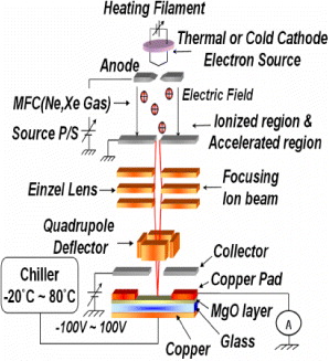
Figure 1 Schematic of the γ-FIB system.
Figure 2 is a schematic diagram showing the Auger neutralization of an approaching He ion with ionization energy E i =24.58 eV towards the MgO surface. When an ion approaches the surface of the MgO single crystal, an electron of the valence band is combined with the ion by a quantum mechanical tunneling effect and an approaching ion is neutralized to become an atom because of the Auger neutralization mechanism. During the neutralization process, the energy for the tunneling electron is transferred to the nearby electrons in the valence band. If the transferred energy to the nearby electrons is either higher or lower than the work function, then the secondary electrons can be emitted from the surface [1].
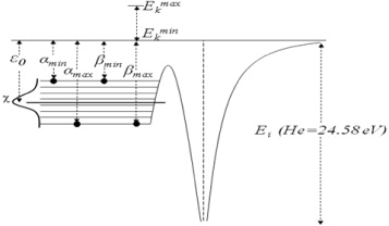
Figure 2 Schematic diagram illustrating the Auger neutralization of an ion at the MgO surface.
We define the characteristic energy spread of electrons in the valence band as χ and ε0 is the band gap energy level located in the center of the valence band in figure 2. The symbol α min in figure 3 is the work function of MgO and we defined α min =ε 0−(χ /2), α max =ε 0+(χ /2) and β is the same as α. If the minimum kinetic energy Ek min from the electrons located at α max and β max is almost close to zero, we can guess that Ek min =E i −(α max +β max )=0 and ε 0=(E i −χ )/2 [1].
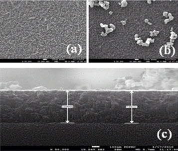
Figure 3 Scanning electron microscopy (SEM) image of MgO thin film with (111) orientation (a), sprayed functional layer on the MgO thin film (b), side view of MgO thin film deposited by 7500 Å (c).
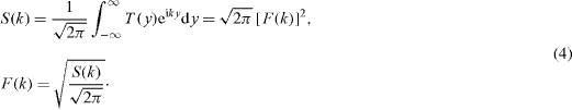
The Auger transform T(Ek ) is defined by

T(Ek ) function is expressed in terms of y=(E i −2ε 0−Ek )/χ as follows:

Substituting the inverse Fast Fourier Transform (IFFT) of f e (x) defined as

we derive the formula for the Fast Fourier Transform (FFT) of T(y),
It is noted that the f
e
(x) in equation (
3. Results and discussion
Figure 3 shows the scanning electron microscope (SEM) images of the MgO thin film surface with (111) orientation (a), sprayed functional layer deposited on the MgO thin film surface (b) and the cutting view of the MgO thin film (c). The thickness of the MgO thin film is about 7500 Å, and the deposition speed is 20 Å s −1 by the electron beam evaporator under the working pressure of 10−5 Torr and the substrate temperature of 300 °C, with (111) crystal orientation. The nano powder for the functional layer (FL) consists of MgO particles whose sizes are around 200 nm. The FL has been sprayed over a 10% area of the MgO thin film by a spray coater.
The total current signals comprising the incident ion and the secondary electron emission currents, detected on the copper pad, versus the collecting voltage in the γ-FIB system are shown in figure 4. The He + ion approaches the MgO thin film, from which the secondary electrons are emitted outside the MgO thin film by Auger neutralization. The secondary electron emission γ is obtained from γ=(I t −I i )/I i [1], where I t is the total current corresponding to the end point of the saturated current signal and I i is the incident ion current corresponding to the starting point of the rapidly increased current signal in figure 4. It is noted that the total current for the sprayed FL on the MgO thin film has a higher saturated current than that for a pure MgO thin film without a FL. The energy spread for the secondary electrons for the MgO thin film is shown to be from 1.45 V to 12.5 V, while it is from 1.45 V to 14.15 V for the sprayed FL. Since the energy spread for the sprayed FL on the MgO thin film is wider by 1.65 V than that for MgO thin film, the sprayed FL on the MgO thin film has larger χ, smaller ε0 and work function (φ(w)) than those for the MgO thin film.
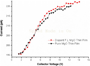
Figure 4 The secondary electron emission current of the MgO thin film (111) surface with and without the sprayed functional layer (FL) with respect to the collector voltage in the γ-FIB system (I/V curve).
Figure 5 shows the Auger transform T(Ek
), which is obtained by differentiating the current signals of figure 4 with respect to the collector voltage, followed by the inversion of the x-axis, since the leftmost collector voltage is the maximum kinetic energy and rightmost saturated collector voltage is the zero kinetic energy of the secondary electrons. We denote the state density function in the valence band by f
e
(x). The Auger transform T(Ek
) is defined as in equation (
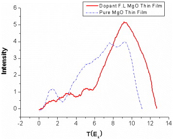
Figure 5 Auger transform T(Ek ) in the MgO thin film and sprayed FL on the MgO thin film.
Figure 6 shows the electron energy band structure in the valence band for an MgO thin film with (a) and without (b) the FL. We can measure the work function φ w , the band gap energy ε0, and the energy band structure f e (x) in the MgO layer with (111) orientation by taking the IFFT to Auger transform function T(Ek ).
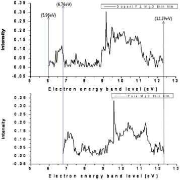
Figure 6 Electron energy band structures of the MgO thin film with (a) and without (b) the sprayed FL.
The electron energy band structure has been measured through the differentiated secondary electron emission current signal and Fast Fourier Transform (FFT) by the γ-FIB system. We discovered that the electron energy band structure includes φ(w), α max , ε0, χ and the distribution of the state density for electrons in the valence band in the MgO surface by the He ion source. We measured the data of the electron energy band structure of the pure MgO thin film and sprayed the FL on the MgO thin film in the valence band. Figure 6 shows that the work function (φ(w)) is 6.09 eV, (ε0) is 9.21 eV, (χ) is 5.9 eV of the sprayed FL on the MgO thin film, and the work function is 6.59 eV (φ(w)), (ε0) is 9.45 eV and (χ) is 5.5 eV in the pure MgO thin film.
Figure 7 shows the result of the secondary electron emission characteristics of the pure MgO thin film and sprayed FL on the MgO thin film by the γ-FIB system. The γ is measured between 130 V and 200 V in a collector per 10 V division. The measured secondary electron emission coefficient of the sprayed FL MgO thin film has a higher value than pure MgO thin film. These observations explain why the sprayed FL on the MgO protective layer plays an important part in ac plasma display panels compared to the films with pure MgO thin film.
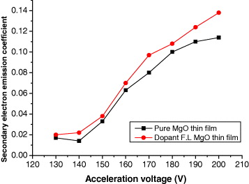
Figure 7 The secondary electron emission coefficient (γ) of the pure MgO thin film and sprayed FL on the MgO thin film by γ-FIB system.
We measured the cathodoluminescence (CL) spectrum intensity of the sprayed 10% nano powder on MgO thin film, pure MgO thin film and 10% nano powder on soda-lime glass. We disregarded the CL spectrum intensity of the glass because the top of that intensity is only 400 between 300 and 400 nm. The sprayed FL on the MgO thin film has a higher CL spectrum intensity than pure MgO thin film (see figure 8). Although the peak of the CL spectrum intensity of sprayed FL MgO thin film consists of pure MgO CL intensity as well as the CL spectrum intensity of the nano powder, the spectrum line is reassemble to the peak of pure MgO thin film. The CL intensity of the nano powder is different from others. However, the sprayed FL on the MgO thin film has only 10% nano powder, so the remainder of the FL area of 90% is the pure MgO thin film. Therefore the nano powder CL spectrum intensity is just added to the pure MgO thin film to yield that for the sprayed FL on the MgO film in figure 8.
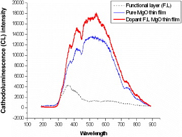
Figure 8 Cathodoluminescence (CL) spectrum intensity of a Functional Layer, pure MgO thin film surface and the MgO thin film with a Functional Layer.
4. Conclusions
We have investigated the electron energy band structure of the sprayed functional layer on MgO thin film by the gamma focused ion beam (γ-FIB) system with a He ion source. The ion-induced secondary electron emission coefficient γ as well as the electron energy band structure depend on the nano powder of the MgO thin film. According to the sprayed FL on the MgO thin film or the non-FL MgO thin film, the secondary electron emission coefficient, electron energy band structure, work function and cathodoluminescence (CL) spectrum intensity are changed. The FL MgO thin film has a low work function (φ(w)) and (ε0) on the other hand has a higher secondary electron emission co-efficient than pure MgO thin film. Therefore these experimental results show that high secondary electron emission co-efficient and low work function FL MgO thin film is more efficient because a low work function and high gamma co-efficient make a low discharge voltage as well as high brightness in a plasma display panel (AC-PDP). The first measurement method to find the start and end point in a secondary electron emission current by a γ-FIB system for the results of T(Ek ), work function, ε0, χ and electron energy band structure is a very important factor in achieving the correct result of this measurement. This system to measure the electron energy band structure of MgO thin film is going to be useful for other insulator thin films, especially applied to CIGS in thin film solar cells.
Acknowledgments
This work was supported by the IT R&D program of MKE/KEIT, KI002179, Development of Eco-friendly 50" Quadro Full HD PDP Technology. It was also partially supported by Kwangwoon University, 2010, and by the Science Research Center program of 20100029418, MEST.