
Abstract
A hybrid plasmonic waveguide consisting of a thin high-index dielectric stripe embedded inside the gap between a metallic substrate and a semiconductor ridge is presented for the purpose of enhanced optical confinement in the gap. By engineering the key geometrical parameters of the stripe, both of the power ratios resided inside the whole gap and the silicon ridge can be enhanced greatly. A power confinement ratio as large as 0.54 in the overall gap region is achievable, for a structure with a 200 nm-wide, 90 nm-thick silicon-stripe embedded in the center of a 100 nm-thick silica gap, which is nearly 50% improvement over that of the corresponding conventional hybrid waveguide. Meanwhile, with the introduction of the 90 nm-thick silicon stripe, the effective mode area of the waveguide exhibits a reduction of 50%–60% with a reasonable propagation length around 25–65 μm for different stripe widths. A study on the influence of possible fabrication imperfections reveals that the modal property is quite robust and highly tolerant to these errors. Such a hybrid plasmonic waveguide with enhanced optical confinement and moderate modal loss may enable the realization of ultra-compact passive components, nanolasers with low pumping thresholds, and other potential applications.
Export citation and abstract BibTeX RIS
1. Introduction
Surface plasmons (SPs) have been regarded as the key to break down the fundamental diffraction limit in conventional photonics systems, as they offer the unique potential to guide and route light at the truly nanometer scale [1]. Along with other attractive properties, such as simultaneously supporting the transmission of light and delivering electric signals through the same chip [2], strong local field enhancement that induces high sensitivity against an index change near metallic surfaces [3], they offer unprecedented opportunities for a number of interesting applications and hold great promise for the realization of on-chip integrations of electronic and photonic components in the foreseeable future [4]. The fascinating goal of guiding and manipulating light at the sub-wavelength scale beyond the diffraction limit has motivated research into the demonstration of various types of SP waveguides capable of achieving diverse functionalities [5–16]. Since these SP-based waveguiding structures play essential roles in determining the performance of integrated photonic components, the simultaneous realization of strong field confinement and low propagation loss has become the hottest pursuit in many of the current studies. One of the most distinguished works among them is the recent demonstration of hybrid plasmonic structures that naturally integrate high-index semiconductor materials and metal waveguides, hence successfully overcoming the conventional constraints imposed by traditional guiding mechanisms in previously studied SPP waveguides, i.e. the fundamental tradeoff between mode confinement and propagation loss [17]. By squeezing the mode field inside the nanometer-size low-index-dielectric-filled gap between the semiconductor and the metal structures, these hybrid devices are able to allow efficient light transmission with simultaneously ultra-low propagation loss and strong optical confinement far beyond the diffraction limit [18, 19]. Their superior optical properties have enabled highly efficient laser action with mode sizes reaching the deep-sub-wavelength scale [20–23], and also facilitated the operation of ultra-compact passive plasmonic devices with complex functionalities [24–34], as well as a number of other useful applications [35–37]. These studies related to hybrid plasmonic structures and components will lay important groundwork for the development of next-generation integrated photonic devices and circuits.
Along with the proposal and demonstration of the above-mentioned hybrid plasmonic components, a number of modified hybrid waveguides with enhanced or unique modal features have also been studied intensively [38–60], including metal-dielectric-slabs [38–43, 51, 60], dielectric-loaded structures [44] coaxial and core-shell [45, 46], wedge or rib type [47–49, 54], nanowire-based waveguides [52, 56, 59] as well as many other forms [50, 53, 55, 57, 58]. In contrast to the prospect of achieving improved optical performance over the conventional hybrid waveguides in a certain aspect, many of these novel structures still face great challenges when leveraged for practical applications. Additional fabrication complexities will render some of the structures rather challenging to realize, which also hinders the migration of these structures from theoretical predictions to practical implementations.
Here, in this work, aiming to enhance field confinement in the gap without introducing much additional fabrication complexity or compromising other important advantages in the modal properties of hybrid SPP structures, we present the design of a novel hybrid plasmonic waveguide by incorporating an additional semiconductor stripe into the center of the gap region. Such a multilayer structure could be realized using planar fabrication techniques and shows the potential to enhance power confinement ratios in both the gap region and the silicon ridge, while still maintaining a low propagation loss and sub-wavelength mode size.
2. Geometries of the hybrid plasmonic waveguide and field distributions
The three-dimensional (3D) geometry of the studied hybrid waveguide is schematically shown in figure 1, where a thin silicon stripe is incorporated at the center of the silica gap between the silver substrate and the silicon ridge. The width and thickness of the silicon ridge are w and h, respectively. The thickness of the silica gap is defined as t and its width as w. The thin silicon stripe has a width of w1 and a thickness of h1, and is assumed to be located at the center of the gap, with an equal distance (gap thickness: g) to either the upper silicon ridge or the lower silver surface. While our simulations also reveal that for the non-equal-gap case, enhanced optical confinement can be achievable as well, for simplicity, in the following investigations we only consider the structure with equal gap thicknesses. The permittivities of silicon, silica, air and silver at the working wavelength of 1550 nm are εd = 12.25, εg = 2.25, εc = 1, and εm =− 129 + 3.3i [61], respectively. The finite element method (FEM) based software COMSOL™ is used to investigate the properties of the fundamental mode supported by the proposed hybrid waveguide. This software has been widely applied to simulate and analyze modal properties of waveguides at telecom wavelengths [18]. In the simulations, scattering boundary conditions with an extremely fine mesh near the gap and the silicon ridge as well as the metal surface are applied to ensure accurate solutions.
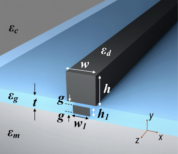
Figure 1. 3D schematic of the studied hybrid waveguide, where an additional silicon stripe with a width of w1 and height of h1 is incorporated at the center of the silica gap (thickness: t), with equal distance (g) to the upper silicon ridge (width: w, height: h) or the metal substrate.
Download figure:
Standard imageThe conventional hybrid plasmonic waveguide is shown to support single quasi-TM mode propagation when the dielectric is not large [18]. Our investigations show that the introduction of the silicon stripe does not influence such a single-mode condition if the silicon stripe is narrow. Figure 2 shows the electric field distributions of the fundamental plasmonic modes supported by hybrid waveguides with and without the silicon stripe, respectively. For both cases, field enhancement occurs in the x and y directions, as shown clearly in the 2D field panels and the cross-sectional plots. A more significantly enhanced electric field is observable in the low-index slot and the gap region of the proposed hybrid waveguide incorporating the silicon stripe. The upper enhancement is mainly caused by the dielectric slot mechanism [62] while the lower enhancement is primarily due to the hybrid effect [18]. Owing to the greatly reduced gap thicknesses, both of the enhancements are seen to be stronger than that achieved without the silicon stripe. It is notable that although enhanced field strength can also be achieved by decreasing the gap thickness of the conventional hybrid structure, the total power confined in the gap would be significantly reduced in that case, as we will discuss in the following part.
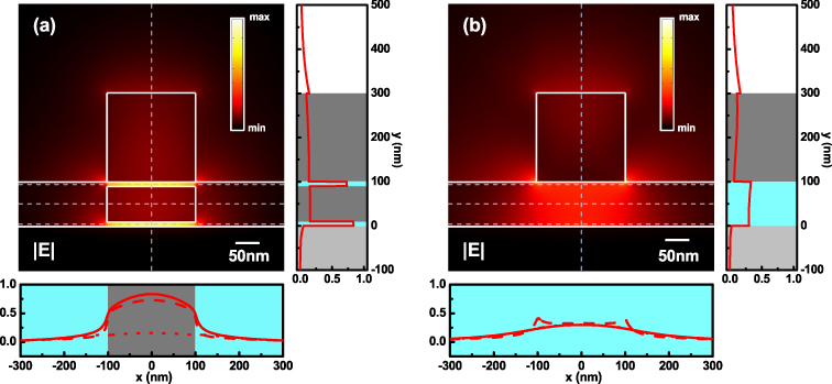
Figure 2. Electric field plots of the hybrid waveguides (a) with the silicon stripe (w1 = 200,h1 = 80 nm) and (b) without the silicon stripe (w = h = 200,t = 100 nm). Fields along the dashed lines in the 2D panel are also depicted to better illustrate the field enhancements. The solid, dotted and dashed lines along the x direction are taken at 5 nm, 50 nm, 95 nm above the silver/silica interface, respectively. Note that, for better comparison, the field distributions of the two waveguides are normalized so that the surface integrals of the power flow in the cross sections are equal. In other words, the same input powers have been assumed for the two modes.
Download figure:
Standard image3. Modal properties of the hybrid plasmonic waveguide
To further illustrate the enhanced field confinement, we quantitatively show the normalized optical power (NOP) and normalized average optical intensity (NAOI) in different regions of the structure. The geometric parameters of the two waveguides are chosen as w = h = 200 nm and t = 100 nm to ensure strong hybridization between the silicon square and the metal surface, while also guaranteeing a near-optimized optical power ratio residing in the gap region for the conventional hybrid waveguide [18]. Here, NOP is defined as the ratio of the power inside the considered region to the total power of the overall waveguide, whereas NAOI is calculated using NOP divided by the area of the corresponding region [44]. The calculated NOPs in the silicon ridge (NOPSi), inside the silica region within the gap (NOPSiO2) as well as in the overall gap domain (NOPgap) are shown in figures 3(a)–(c) for different stripe sizes, where the definitions of the silica and gap regions are also illustrated schematically in the insets. Here, NAOI in the silicon ridge or the silicon stripe is not shown directly in the figures, due to its relatively small value [62]. When w1 is small (e.g. w1 ≤ 200 nm), NOPSi experiences a monotonic increase when h1 gets larger, indicating improved confinement is achieved in the silicon ridge incorporating a thicker silicon stripe. On the other hand, as the silicon stripe width exceeds that of the gap region, the increasing trend of NOPSi slows down and finally turns into a reverse one, i.e., exhibiting reduced confinement in the ridge when the stripe is relatively wide (e.g. when w1 > 400 nm). The power ratio confined in the silica region within the gap (see the inset in figure 3(a)) shares a similar trend for different w1. As seen in figure 3(b), NOPSiO2 increases first, before decreasing when h1 becomes larger. It is also illustrated that the critical thickness (where the trend changes) is different for various stripe widths. When w1 is small (e.g. w1 = 50 nm), the size of the silica region remains almost unchanged even if h1 gets close to the thickness of the whole gap (t). This is the reason why NOPSiO2 maintains a relatively large value during the variation of h1, with the reversing of the increasing trend occurring at a large h1. On the other hand, for the large w1 case (e.g. w1 ≥ 200 nm), the silica area shrinks dramatically with an increased h1, which leads to a significantly weakened confinement in the silica region and hence a rapid reduction of NOPSiO2. Corresponding to the result of NOPSiO2, the trend of different NAOISiO2 for different stripe widths may also be explained, which can be simply attributed to the difference between the decreasing speed of the power ratio and the reducing speed of the silica size. On the one hand, for narrow silicon stripes (w1 < 200 nm), the field enhancements in silica gaps between the stripe and its adjacent surfaces could be significant when h1 is relatively large (e.g. see figure 3(g)). However, strong enhancements only occur perpendicularly near the surfaces of the stripe and weaken rapidly in both directions along the x axis inside the gap, due to the discrepancy between the stripe width and the ridge width. Therefore, in the overall silica region inside the whole gap (including the subdomains on both sides of the stripe besides the upper and lower silica gaps), the calculated NAOISiO2 is greatly compromised by the low intensities in other areas of the gap and hence could not experience a dramatic increase as h1 gets larger. On the other hand, when w1 exceeds 200 nm, the field enhancements are observable in all the silica regions inside the gap (see figures 3(h) and (i)), which results in dramatically increased optical intensity at thicker stripes and consequently leads to the extremely high NAOISiO2 when h1 are very large.
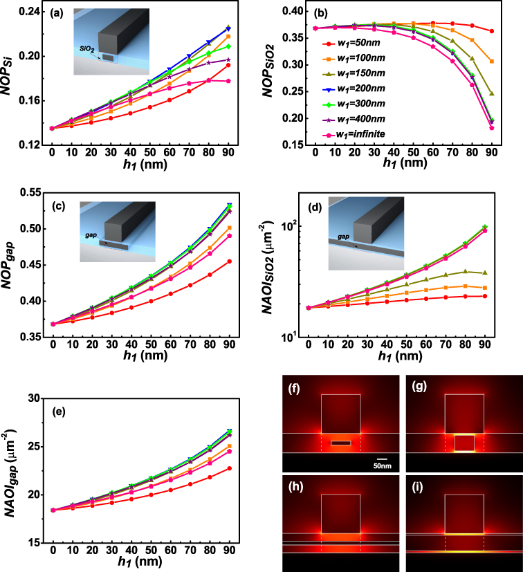
Figure 3. (a)–(e) Normalized optical power (NOP) and normalized average optical intensity (NAOI) in different regions of the studied hybrid waveguide with various silicon stripe sizes: (a) NOP in the silicon ridge (NOPSi); (b) NOP in the silica region within the gap (NOPSiO2); (c) NOP inside the gap (NOPgap); (d) NAOI in the silica region (NAOISiO2); (e) NAOI inside the gap (NAOIgap); (f)–(i) electric field distributions of the hybrid modes supported by waveguides with different stripe widths: (f) w1 = 100 nm,h1 = 20 nm; (g) w1 = 100 nm,h1 = 80 nm; (h) w1: infinite, h1 = 20 nm; (i) w1: infinite, h1 = 80 nm. The scale bars for (f)–(i) are the same.
Download figure:
Standard imageInterestingly, for the power ratio and intensity inside the overall gap (shown in figures 3(c) and (e)), a monotonic increase trend is always observable for all the considered stripe widths as h1 gets larger. The largest values of NOPgap and NAOIgap are achieved at w1 ∼ 200 nm, where the silicon stripe and ridge have the same width. For the extreme case of w1 = 200 nm and h1 = 90 nm, normalized optical powers as large as 0.54 in the overall gap region and 0.23 inside the silicon ridge are possible to achieve. These values are nearly 50% and 70% improvements over the respective power ratios of the corresponding conventional hybrid waveguide (i.e. h1 = 0 nm). The enhancement could be even larger through further increasing the stripe thickness (e.g. h1 can be increased up to 96 nm, corresponding to 2 nm-thick silica gaps on both sides of the stripe). The strong field confinement in the high-index region of the waveguide could facilitate its applications in active devices. For instance, a gain medium can be incorporated either in the upper silicon ridge or in the silicon stripe, to realize loss compensation and the operation of plasmon nanolasers. For the silicon ridge, the pump light can be incident from the cladding to excite the gain material. While for the silicon stripe, the gain medium may also be excited by introducing pump light from the side of the waveguide, although it might present some additional challenges in implementation. It is worth mentioning that, when the gap distance between the silicon stripe and the metal substrate is very small (e.g. less than 5 nm), the exciton recombination is too close to the metal surface, which might cause rapid non-radiative quenching and would greatly hinder effective operation of active devices, similar to other active plasmonic waveguides and components [20, 63]. We note that the local field enhancement in the gap region could also be strengthened simply by reducing the gap thickness of the conventional hybrid plasmonic waveguide (without the incorporated silicon stripe). However, the total power located inside the gap in that case would drop dramatically due to the rapid reduction of the gap area. For instance, for the traditional hybrid structure with a 5 nm-thick gap, there is only 0.1749 of the total power stored in the gap, much smaller than that achieved using the proposed waveguide.
We then show the dependence of modal properties on the size of the silicon stripe by varying w1 and h1, while the width of the square-shaped silicon ridge is fixed at 200 nm and the gap thickness remains at 100 nm. Neff is the complex modal effective index and neff is the real part of Neff. The propagation length is obtained by L = λ/[4πIm(Neff)], whereas the effective mode area is calculated using Aeff = (∬W(r)dA)2/(∬W(r)2dA) [64]. In order to accurately account for the energy in the metal region, the electromagnetic energy density W(r) is defined as [18]

In equation (1), E(r) and H(r) are the electric and magnetic fields, ε(r) is the electric permittivity and μ0 is the vacuum magnetic permeability. A0 is the diffraction-limited mode area in free space and defined as λ2/4. The normalized mode area can thus be obtained by calculating Aeff/A0. As shown in figures 4(a)–(c), monotonic trends are observed in neff and L for all the studied cases. Increasing w1 or h1 results in an increase in neff and a reduction of the propagation length. The trend of the mode area, however, is relatively more complicated. Waveguides with larger h1 usually have smaller mode areas, indicating the possibility for further downscaling of the mode size using thicker silicon stripes. On the other hand, different trends are observed during the increase of the stripe width. When w1 < 200 nm, a wider silicon stripe corresponds to a smaller Aeff. However, as w1 becomes relatively large (w1 ≥ 200 nm), the mode area will increase with the widened silicon stripe due to the gradually increased optical power confined in the wide-silicon-stripe region. Yet such an increase in mode size is not large owing to the maintained overall confinement, with most of the power confined in the gap and ridge, which makes the waveguide quite robust against changes of the stripe width. Within the considered geometrical range shown in figure 4, long-range propagation could be achieved along with sub-wavelength mode confinement. For the extreme case of h1 = 90 nm, a reduction of 50%–60% in the mode area is observable compared to the conventional hybrid waveguide (h1 = 0 nm), while the corresponding propagation length is still relatively large (25–65 μm).
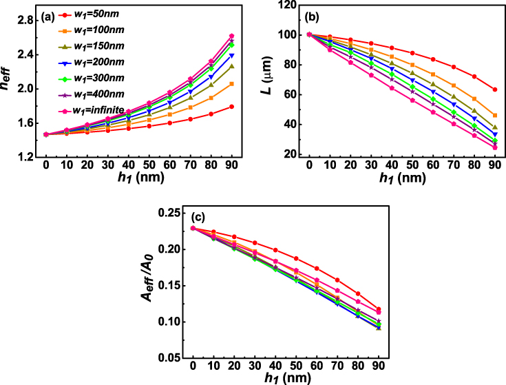
Figure 4. Dependence of the modal characteristics of the studied hybrid waveguide on the silicon stripe size: (a) modal effective index (neff); (b) propagation distance (L); (c) normalized mode area (Aeff/A0).
Download figure:
Standard imageTo fabricate such a waveguide, methods similar to those conventional hybrid plasmonic waveguides can be employed [19, 20]. The only difference is the formation of the additional thin silicon stripe inside the gap, which could be realized by adopting additional deposition and patterning/etching steps (for the infinite wide stripe case, only depositions are needed). The vertical position of the silicon stripe, which is determined by the thickness of the silica layer above and beneath the stripe, can be controlled with relatively high accuracy, as indicated in previously demonstrated multilayer horizontal slot waveguides [65]. In contrast, the lateral position of the stripe is more challenging to control. Due to the fact that the silicon ridge and the stripe are fabricated in different patterning steps, an accurate alignment between them is rather difficult, which may cause the silicon stripe to deviate laterally from the center of the gap region. Therefore, in the following part, we carry out further investigations on the mode's properties against the variation of such a lateral position. The lateral misalignment of the silicon stripe with respect to the center of the waveguide is denoted as δx (see the inset of figure 5(a)). Due to the symmetric waveguide geometry with respect to the x axis, lateral misalignment in either direction (left or right) will exert a similar effect. To be succinct, in the following discussions, we only consider the displacement in the right direction (δx > 0). From the calculated results shown in figure 5, it is clearly seen that the variation of δx from 0 to 50 nm induces small modifications in the effective index, propagation distance and the mode area for all the studied configurations. For example, 1.5% and 2.2% changes in L and Aeff respectively are observed for a waveguide with a 200 nm-wide, 50 nm-thick silicon stripe having a lateral displacement of 50 nm. Despite the slightly asymmetric modal profile (see figure 5(g)), the modal characteristics remain excellent, with sub-wavelength mode confinement and long-range propagation distance. By contrast, the normalized optical power and average optical intensity seem to be slightly more sensitive to the changes of the lateral position, especially when the silicon stripe is relatively narrow and thick. Considering a stripe with w1 = 100 and h1 = 90 nm, for example, a 50 nm misalignment induces a 2.63% fluctuation in NOPSi and a 5.91% variation in NOPgap. While the corresponding changes are 4.28% for NOPSi and 4.31% in NOPgap for a 200 nm-wide, 90 nm-thick silicon stripe. These relatively obvious variations are primarily due to the greatly modified hybridization between the dielectric modes and the plasmonic mode in such a highly asymmetric geometry (see figures 5(h) and (i)). In the above cases, although the confinement in the ridge and the gap is weakened to some extent under this lateral misalignment, the absolute values of NOPSi and NOPgap are still at a relatively high level, indicating a reasonable tolerance of the modal properties against such a fabrication imperfection. On the other hand, for wide silicon stripes (e.g. w1 = 400 nm), the lateral displacement results in slight changes in the modal properties as well as small modifications in the mode's profile even when h1 gets as large as 90 nm. This is due to the unchanged silicon stripe geometry located inside the gap region, which helps maintaining the strong interaction between the silicon stripe and the adjacent structures (i.e. silicon ridge and metal substrate), as also illustrated in the corresponding field distributions (see, for example, figure 5(j)). In summary, the overall property of the waveguide can be deemed robust against lateral misalignment of the embedded silicon stripe, which is certainly beneficial for its further implementations.
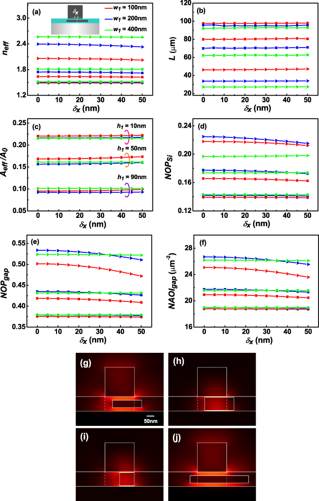
Figure 5. Dependence of modal properties on the lateral misalignment (δx): (a) modal effective index (neff), where the inset shows the corresponding 2D geometry with a laterally displaced silicon stripe; (b) propagation distance (L); (c) normalized mode area (Aeff/A0); (d) normalized optical power in the silicon ridge (NOPSi); (e) normalized optical power in the gap (NOPgap); (f) normalized average optical intensity in the gap (NAOIgap). The gap region is defined the same as before, with a lateral boundary as depicted in dashed lines. Red curves for w1 = 100 nm, blue curves for w1 = 200 nm, green curves for w1 = 400 nm; round symbol: h1 = 10 nm, square symbol: h1 = 50 nm, triangular symbol: h1 = 90 nm. (g)–(j) Mode profiles (electric distributions) for typical configurations: (g) w1 = 200 nm, h1 = 50 nm, δx = 50 nm; (h) w1 = 200 nm, h1 = 90 nm, δx = 50 nm; (i) w1 = 100 nm, h1 = 90 nm, δx = 50 nm; (j) w1 = 400 nm, h1 = 50 nm, δx = 50 nm. The scale bars for (g)–(j) are identical.
Download figure:
Standard image4. Conclusions
In this paper, we have investigated the optical performance of a novel hybrid plasmonic waveguide that incorporates a silicon-stripe-embedded-silica-gap sandwiched between a square silicon ridge and a metal plane. Through systematic analysis using the finite element method, enhanced optical confinement in both the gap region and the silicon ridge is demonstrated with a reduced mode area and moderate propagation loss. Considerations of practical fabrication issues also reveal the robustness of the modal property against possible fabrication errors. Such a structure with improved field confinement may enable the implementation of plasmonic interconnects with rather low crosstalk and also facilitate the realization of various ultra-compact passive components. Highly efficient active plasmonic devices may also be realized by possible incorporation of a gain medium, offering the potential for surface plasmon amplification and nanolasing.
Acknowledgments
The work at Beihang University was supported by 973 Program (2009CB930702), NSFC (61221061/61077064), National Key Scientific Instruments and Equipment Development Special Fund Management (2011YQ0301240502) and the Innovation Foundation of BUAA for PhD Graduates.