
Abstract
We present ultraviolet–visible (UV/vis) range photodetectors (PDs) based on thin film ZnO (n)/Si (p) heterojunction diodes. ZnO films are grown by the atomic layer deposition (ALD) technique at growth temperatures of 80, 150, 200 and 250 ° C. The fabricated ZnO (n)/Si (p) photodetectors (ZnO–Si-PDs) show good electrical rectification characteristics with ON/OFF ratios reaching up to 103. Under UV (350 nm wavelength) and visible (475 nm wavelength) light illumination, the ZnO–Si-PDs give photoresponsivity values of 30–37 mA W−1 and 74–80 mA W−1 at 0.5 V reverse bias, respectively. Photoluminescence (PL) spectra of ALD grown ZnO thin films are used to support the results.
Export citation and abstract BibTeX RIS
1. Introduction
Currently, the capabilities of modern electronic and photonic devices are being extended by the emerging field of thin film semiconductor materials. Thin film optical photodetectors that work in the ultraviolet and visible (UV/vis) range have been fabricated based on semiconductor nanomaterials [1, 2]. Among these semiconductor materials, ZnO is also attractive for thin film photodiode applications. ZnO is a non-toxic material which can be deposited at low temperatures with good crystalline quality which provides advantages in photodiode and solar cell applications [3, 4]. Besides being optically transparent and electrically conductive, this material has the ability to increase the path of the light within a fabricated solar cell or a photodiode due to its surface roughness [4]. ZnO has a direct wide bandgap of 3.3 eV which makes the absorption of high energy photons possible within a fabricated photodiode or solar cell, which increases the efficiency of the fabricated device [5–9].
It is possible to deposit ZnO on various substrates using low pressure chemical vapour deposition (LPCVD) [4], RF magnetron scattering [6–8, 10], DC magnetron scattering [11], metal organic chemical vapour deposition (MOCVD) [12, 13] or the spray pyrolysis method [14]. Fay et al fabricated p–i–n microcrystalline Si:H solar cells using LPCVD grown ZnO [4]. In addition, it is possible to fabricate n-ZnO/p-Si photodiodes based on n-ZnO that is obtained through RF sputtering [3, 6, 7, 10]. Kim et al fabricated n-ZnO/p-Si photodiodes based on n-ZnO thin films obtained through RF sputtering, and they reported a maximum photocurrent density value of 11 mA cm−2 under 5 V reverse biasing conditions [3].
A promising method for depositing ZnO thin films on various substrates is the atomic layer deposition (ALD) method [15–21]. The ALD deposition of ZnO takes place in a reaction chamber by cycling sequential half-reactions of diethylzinc (DEZn) and water vapour (H2O) precursors, which leads to the formation of ZnO thin films with excellent uniformity and conformity [22, 23]. Despite the above mentioned works involving the use of ZnO that is grown by various methods in photodiode applications, there is no work reported in the literature regarding the use of ALD grown n-ZnO thin films on p-type silicon substrates as photodiodes or solar cells. In this work we present ultraviolet–visible range photodetectors based on ALD grown thin film ZnO (n)/Si (p) diodes. The effect of ALD growth temperature (80–250 ° C) is investigated using dark current and photoresponsivity analysis. The results are supported by PL measurements of the grown films.
2. Experimental details
ZnO–Si-PD fabrication was performed on highly doped p-type (0.1–0.9 Ω cm boron doped) Si substrates. The substrates were cleaned using acetone, isopropanol and de-ionized water. ZnO layers were deposited on p+-Si substrates by ALD using a Cambridge Nanotech Savannah 100 type commercial reactor in vacuum conditions, under 1 Torr base pressure. The growth temperatures were 80, 150, 200 and 250 ° C. Diethlyzinc (DEZn) and water vapour (H2O) were used as ALD precursors and the growth was carried out for 300 cycles at each temperature. The ZnO ALD growth parameters are given in table 1. The top contacts were formed by evaporating 100 nm of Al and patterning by the lift-off technique. No annealing was performed during the metallization process. A blanket Al layer was used as the back contact to form vertical ZnO (n)/Si (p) heterojunction diodes. The PL spectra of the ALD grown ZnO (n)/Si (p) samples were recorded with a Varian Eclipse type fluorescence spectrophotometer.
Table 1. ALD growth parameters at different growth temperatures.
| Temperature (° C) | Pulse time (s) | Purge time (s) | Deposition rate (Å/cycle) |
|---|---|---|---|
| 80 | 0.015 | 60 | 1.28 |
| 150 | 0.015 | 60 | 1.51 |
| 200 | 0.015 | 10 | 1.49 |
| 250 | 0.015 | 5 | 1.15 |
3. Results and discussion
Figure 1(a) shows a schematic illustration of a ZnO–Si-PD. The bottom and top Al layers are used as the front and back electrodes. Figure 1(b) shows a scanning electron microscope (SEM) image of a fabricated ZnO–Si-PD. The top Al layer consists of 5 μm wide finger structures with 5 μm gaps between fingers, which allow light penetration into the fabricated device. The measured resistivities of ZnO films, plotted in figure 2, are in good agreement with the literature [24].

Figure 1. (a) Schematic illustration of the fabricated ZnO–Si-PD. (b) SEM image, top view of the fabricated ZnO–Si-PD.
Download figure:
Standard image High-resolution image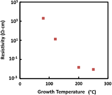
Figure 2. Measured thin film resistivities of ZnO films for different growth temperatures.
Download figure:
Standard image High-resolution imageFigure 3 shows the PL spectra of ZnO thin film layers grown on p+-Si substrates. The PL spectra were obtained with 250 nm (figure 3(a)) and 390 nm (figure 3(b)) wavelength excitations. The 250 nm excitation gave PL emission peaks at 376 nm, 426 nm and 500 nm. The bandgap energy of ZnO is reported as 3.3 eV, which agrees well with the PL peak at 376 nm. The PL signal at 426 nm is believed to be due to 'band edge' excitonic states [17]. The PL signal at 500 nm is due to the strong reflection of the second order harmonic of the excitation source beam. These results are in accord with the PL measurements under 390 nm excitation where a single band edge PL emission peak at 418 nm is obtained. Since 390 nm excitation is not sufficient for band-to-band excitation, the second peak around 376 nm did not appear. The sharp and distinct PL signals confirm the formation of good crystalline quality ZnO thin films by ALD, which is important for device applications [17].

Figure 3. PL spectra of ALD grown ZnO thin films (80, 150, 200, 250 ° C). (a) At 250 nm excitation, (b) at 390 nm excitation.
Download figure:
Standard image High-resolution imageIt is a well known fact that unintentionally doped ZnO layers exhibit n-type behaviour due to crystal defects such as oxygen vacancies and interstitial zinc, although there is still debate on the exact mechanisms of the contribution of defects to charge carrier concentration. The electrical characterization of the fabricated ZnO (n)/Si (p) heterojunction diodes was made with a commercial Keithley 4200-SCS type semiconductor parameter analyser. The current–voltage (I–V) characteristics were obtained under dark conditions, as shown in figure 4. The ZnO–Si heterojunction diodes show the highest rectification for 80 ° C-grown ZnO, which has the lowest doping (highest resistivity). Such a junction is ZnO-n/Si-p+ and exhibits good electrical rectification characteristics with ON/OFF ratios reaching up to 103. For heterojunctions formed by ZnO films grown at higher temperatures, the resistivity of the ZnO films becomes comparable to or even less than the silicon substrate; therefore, the thin space charge region is expected on the silicon side.

Figure 4. Dark current (I) versus bias voltage (V) spectrum of the ZnO–Si-PDs.
Download figure:
Standard image High-resolution imageThe spectral photogenerated current (Iphoto) was measured with mechanically chopped, monochromated light normally incident on the device surface and a lock in amplifier (SRS 830). The incident light power (Pin) was measured with a calibrated Si photodetector. Figure 5(a) shows photoresponsivity versus applied voltage (obtained under 0–0.5 V reverse biasing conditions) under illumination with λ = 350 nm light. The illumination power at this particular wavelength was 5.84 × 10⁻⁵ W. There is a sharp increase in photoresponsivity values up to 0.2 V reverse bias. However, the photoresponsivity values remain constant within the 0.2–0.5 V reverse biasing range, which indicates a saturation in photoresponsivity values. This is attributed to efficient collection of photogenerated carriers with applied bias and eventual saturation of the carrier drift velocity due to random scattering events. At this particular wavelength, the ZnO–Si-PDs gave photoresponsivity values of 37 mA W−1 (80 ° C), 35 mA W−1 (250 ° C) and 30 mA W−1 (150, 200 ° C) under 0.5 V reverse biasing conditions. The highest photoresponsivity value obtained with an ALD growth temperature of 80 ° C could be attributed to the best O:Zn stoichiometric ratio at this particular growth temperature [23]. At higher ALD growth temperatures oxygen content decreases, which reduces the O:Zn stoichiometric ratio [23]. However, temperature related variations in the O:Zn stoichiometric ratio do not cause large changes in the photoresponsivity values. Figure 5(b) shows photoresponsivity versus voltage data (obtained under 0–0.5 V reverse biasing conditions) under illumination with λ = 475 nm light. The illumination power at this particular wavelength was 8.88 × 10⁻⁵ W. The bias voltage dependence of the photoresponse is similar to the UV-illuminated case, which exhibits an increased response until 0.2 V and saturation for larger reverse bias voltages. At this wavelength, the ZnO–Si-PDs gave photoresponsivity values of 80 mA W−1 (150, 200 ° C) and 74 mA W−1 (80, 250 ° C) under 0.5 V reverse biasing conditions. Figure 6 shows the spectral photoresponsivity data obtained within the 300–1000 nm wavelength range under 0.5 V reverse biasing conditions. The maximum photoresponsivity values of 90 mA W−1 (150, 200 ° C), 85 mA W−1 (80 ° C) and 84 mA W−1 (250 ° C) were observed at 585 nm. Figure 6 shows that the ZnO–Si-PDs operate well in the UV range as well as in the vis range. Since a space charge region exists in silicon for highly doped ZnO films (higher growth temperatures), optical absorption in the silicon also contributes to the visible photoresponsivity. In addition, at longer wavelengths, the photoresponsivity decrease is consistent with the silicon absorption band edge (around 1100 nm).
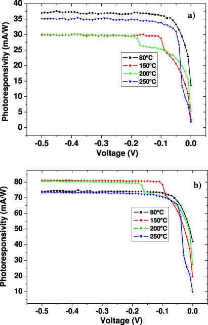
Figure 5. (a) Photoresponsivity versus voltage spectrum at 350 nm wavelength. (b) Photoresponsivity versus voltage spectrum at 475 nm wavelength.
Download figure:
Standard image High-resolution image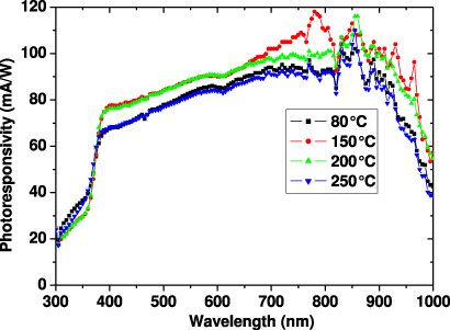
Figure 6. Photoresponsivity versus wavelength (300–1000 nm) spectrum at 0.5 V reverse bias.
Download figure:
Standard image High-resolution image
4. Conclusion
In summary, UV/vis range photodetectors were experimentally demonstrated using ZnO thin films that were obtained through ALD at various growth temperatures. The fabricated ZnO–Si-PDs showed good electrical rectification characteristics and operated well within the 300–1000 nm wavelength range. It was shown that the photoresponsivity values could be tuned by changing the ALD growth temperatures, which is important for commercial photodetector applications. Moreover, these results highlight the use of ALD grown ZnO thin films in next-generation photodetector and photovoltaic device applications.
Acknowledgments
The State Planning Organization (DPT) of Turkey is acknowledged for the support of the UNAM-Institute of Materials Science and Nanotechnology. Dr Okyay acknowledges European Union Framework Program 7 Marie Curie IRG Grant 239444, COST NanoTP, TUBITAK Grants 109E044, 112M004 and 112E052. The authors thank Mr Semih Yaşar for his kind support with cleanroom experiments. The authors also thank Mr Adem Saraç for his help with electron microscopy imaging.