


Abstract
As the key concept in fabricating integrated device, surface plasmon-polaritons (SPPs) have been widely employed to artificially manipulate the electromagnetic waves in metallic surfaces. However, due to the highly structure-dependent resonance of SPPs, it is challengeable to develop a fixed device which can function at wide band. Here, we propose a novel broadband and robust SPPs directional coupler based on the tri-layered curved waveguides working at terahertz (THz) frequencies, where the coupling of SPPs between the adjacent waveguides can be modeled with coupled mode theory. By introducing the stimulated raman adiabatic passage quantum control technique, we achieve the complete transfer of SPPs from the input to the output waveguides in the range of 0.9–1.3 THz, and even considering the propagation loss, the transfer rate is still above 70%. Furthermore, the performance of our device is eminently robust because of its insensitivity to the geometry of structure and the wavelength of SPPs. As a result, our device can tolerate defect induced by fabrication processing and manipulate THz waves at broadband. This finding provides a new theoretical guideline in promoting THz on-demand applications, which is of significance in developing integrated THz devices.
Export citation and abstract BibTeX RIS

Original content from this work may be used under the terms of the Creative Commons Attribution 3.0 licence. Any further distribution of this work must maintain attribution to the author(s) and the title of the work, journal citation and DOI.
1. Introduction
Terahertz (THz) radiation has drawn enormous attentions these years. Since many material responses are located at THz frequencies, THz technologies can obtain unique spectral characteristics and abundant information about matters, which is widely used in spectroscopy [1] and imaging [2]. Naturally, the THz applications in information processing and transmission [3, 4] are vital. On the other hand, with the rapid development of the network and popularization of portable terminals, the miniaturization of the integrated devices is an irresistible trend. THz technologies are promising to accelerate the next generation of communications [5–7] due to the capabilities of high information capacity and micro-size [8, 9]. To realize further integration, how to manipulate the electromagnetic (EM) waves in subwavelength scale is a principal issue. Surface plasmon polaritons (SPPs) are the EM waves propagating along metal-dielectric interfaces with exponential decay in the direction perpendicular to the interfaces. The recent emerged SPPs-based elements, such as antennas [10, 11], waveguides [12, 13] and logic circuitry [13, 14], demonstrated their potential application on the microscale and nanoscale chips since the wavelength of SPPs can be scaled down below diffraction limit [15–17]. Thus, employing SPPs is the essential approach for designing compact integrated THz functional devices.
At THz regime, SPPs-based waveguides [18], couplers [19] and coders [20] have been investigated recently, which make great contributions to the THz applications. Due to the much smaller wavelength of SPPs at THz regime, complete transfer of energy and information via SPPs is significant to implement compact devices in THz regime. Two recent researches studying on the coupling of THz SPPs waveguides [18, 21] involved in coupled mode theory (CMT), which is a widely used theory in describing coupling between two optical waveguides, through the overlap of their evanescent electromagnetic fields [22, 23]. Base on this concept, if two thin films are close enough, the two evanescent fields of SPPs in each thin film have overlapping and SPPs can transfer from one thin film to another [18, 21]. In our paper, we employ and derive the CMT to describe the SPPs coupling between corrugated thin films structure. Significantly, we derive the Schrödinger-like equation of SPPs coupler from the coupling equation based on CMT.
However, the present stuctures of two parallel THz SPPs waveguides (e.g. [18, 21]) require rigorous fabrication precision and only operate at specific excited frequency of THz waves, otherwise, the fidelity of device will drop rapidly. Consequently, current THz SPPs-based devices are facing the problems of high-cost fabrication processing and narrow transferring band. Most recently, to overcome this shortcoming, a remarkable paper applied coherent quantum control (stimulated raman adiabatic passage, short for STIRAP) into transferring the SPPs on the graphene sheets [24]. STIRAP is the well-known three-level coherent quantum control, which completely transfers population from first state to third state, without any population remaining in intermediate state [25, 26]. Furthermore, it is shown that STIRAP is exceedingly robust against controlling parameters under perturbations. The SITRAP has already been widely used in various domains, such as atomic molecular and optical physics [27, 28], waveguide coupler [29, 30], graphene electronic and optical effect [24, 31].
In this paper, we firstly introduce the STIRAP technique into the SPPs waveguide coupler at THz regime, to achieve very robust device against varying frequency of input THz waves and disturbances on the geometry parameters. We propose the tri-layered corrugated thin film coupler structure with some curved configuration to obtain the STIRAP coupling scheme and we substantiate that the performance of our coupler is also robust to the geometry of device and wavelength of SPPs. As a result, our device can tolerate defect induced by fabrication and manipulate THz wave at broadband, which not only can prominently reduce the expenditure of fabrication but also obtains versatile THz devices, due to its operation for broadband THz wave. We believe our design is meaningful in developing THz integrated devices.
2. Schrödinger-like equation of SPPs coupler
We first consider THz radiation to excite SPPs on the surface of the corrugated thin films structure, with working as the waveguide. Assuming the slab corrugated thin films locate at z = 0 at x, z plane, we illuminate the THz waves on the surface of the thin film to excite SPPs propagating along x direction. In order to extend the propagation distance of SPPs, it is remarkable to utilize corrugated structure cutting on the thin film [18, 21], as shown in figure 1, with cutting depth h, width a, period d and thickness of thin film t. If we contemplate the mode profile of SPPs, electric field of SPPs has exponentially decay along with y and z directions outside the SPPs waveguide, as the evanescent field of electric field.

Figure 1. (a) The enlarge view of the corrugated structure of thin film. (b) Two parallel corrugated thin film place at z = g/2 and z = −g/2, where g is the gap distance between two thin films.
Download figure:
Standard image High-resolution imageIn this paper, we only study the coupling mechanism along z direction. Therefore, the electric field along the SPPs propagation direction (x direction) and the evanescant field in z derection are observed and we ignore the electric field of y direction. Assume that we place two corrugated thin films at z = g/2 and z = −g/2 and these two films are parallel to x, y plane, where g is the gap distance between two parallel thin films (see figure 1). The TM polarized SPPs modes are excited on one corrugated thin films. The electric fields can be described by  and
and  . Here km is the decay rate of evanescent field in the surrounding dielectric mediums, given by
  [32].
[32].  m is the permittivity of medium material (we use silicon as surrounding mediums) and ω is the frequency of incident wave in air. In addition, q is the propagation constant of SPPs and it well depends on the geometric parameters of the structure and frequency of incident THz wave ω [18, 19, 33]. We can numerically solve it by dispersion equation, given by
  [33].
[33].
In our parallel coupling model, we take the notations Ψ1(x, z) (Ψ2(x, z)) as the electric field of SPPs on the first (second) thin film, written as

where a1(x) and a2(x) are the amplitudes of the modes with respect to SPPs on two thin film. Due to the extremely thickness of film (t = 100 nm) comparing to other geometry parameters, we can obtain the mode profiles of SPPs as  and
and  . The electric filed have to be normalized by the normalization factor as
  for the thin film 1 and 2, respectively. We take the notation as ψ1 =
  and ψ2 =
  , where ψ1 and ψ2 must be satisfied Helmholtz equations in the x direction.
Based on the CMT model, we can manipulate the Helmholtz equations with the source terms to obtain

where  with thin film (gold) permittivity g. These equations are consistent with the conventional optical waveguide coupled equations [32].
By substituting the wave functions of the SPPs on two thin films into the given Helmholtz equations, we simplify the formation by using the slowly varying envelope approximation [32], namely  and
and  . Thus, we can ignore the second order differential terms and obtain the equation (3) from equation (2). Under this approximation, the coupling equations can be rewritten as a Schrödinger-like equation of a two-level system, given by

Here, C12 and C21 are the coupling coefficients:  and
and  .
.
Beneficial to illustrate trends of the coupling strength against to different parameters, we demonstrate coupling strength against varying gap distance and cutting depth h (see figure 2(a)). Furthermore, figure 2(b) shows the coupling strength as the function of changing frequency of input THz radiation and gap distance. From results of figure 2(a), the coupling strength will exponentially decrease either by increasing gap distance or by increasing the period d. It is remarkable to attain that escalating the frequency of input THz radiation will enhance the coupling strength from 0.2 to 1 THz, shown in figure 2(b). These results are noticeably the same as the trends of the SPPs' coupling strength on two parallel thin film structure [21]. As an example, it is straight forward to obtain the coupling strength C12 = C21 = 1590 m−1, with setting up a = 40 μm, d = 50 μm, h = 30 μm, g = 2 μm and input frequency of THz waves at 1 THz, which is the first point of red line in figure 2(a).
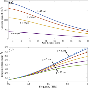
Figure 2. We set the a = 40 μm, d = 50 μm. (a) The coupling strength against varying gap distance and height of corrugated structure, with input frequency of terahertz waves at 1 THz. (b) The function of coupling strength with changing frequency of input terahertz radiation and gap distance with h = 30 μm. The dashed line is with case g = 2 μm and solid lines are with cases from g = 5 μm to g = 25 μm.
Download figure:
Standard image High-resolution imageIn our first example, we only consider SPPs coupling between two corrugated thin films. Based on the coupling equation of bi-layered SPPs coupling equation (3), it is obviously to extend the SPPs coupling among multi-layered thin films by using analogy of multi-level Schrödinger equation, written as

Here, C12(x) (C21(x)) is the coupling strength of SPPs between first and second layer corrugated thin film and Cn−1,n(x) (Cn,n−1(x)) is the coupling SPPs between (n − 1)th and nth layer thin film. Similarly, a1 and an are the SPPs amplitudes of first and nth corrugated thin film.
3. Adiabatic following SPPs on tri-layered thin film coupler
In this paper, we take the tri-layered thin film coupler as simulating three-level atomic quantum system by employing STIRAP. Thus, based on the multi-layered SPPs coupling equation (4), the coupling equation for tri-layered SPPs coupler is described as

where a1 (a2, a3) is the power amplitude of the first (second, third) SPPs waveguide. C12 (C23) is the coupling strength between first and middle layer (middle and third layer), where  and C23 = C32 = Ω2. According to theory of STIRAP, it is conventional to change the normal base into the adiabatic base, where the eigenvalues are

and the corresponding eigenstates are

where the mixing angle θ is given by  . The adiabatic state set
 ![${[{\phi }_{+},{\phi }_{0},{\phi }_{-}]}^{\dagger }$](https://content.cld.iop.org/journals/1367-2630/21/11/113004/revision2/njpab4d91ieqn17.gif) can be transferred from diabatic state set [a1, a2, a3]† with rotation matrix R(t), as
can be transferred from diabatic state set [a1, a2, a3]† with rotation matrix R(t), as

Substituting this rotation matrix R(t) into the time dependent Schrödinger equation equation (5) obtains time dependent Schrödinger equation with adiabatic state and reads

where Ha is the adiabatic Hamiltonian, given by  and over-dot means derivation of time. In terms of rotation matrix R(t), we read the adiabatic Hamiltonian Ha

Thus, if it satisfies adiabatic following condition ( ), we can ignore the off-diagonal terms of adiabatic Hamiltonian Ha. Therefore, there is no transition between adiabatic states with evolving time evolution.
At the beginning of the STIRAP scheme, the Ω2 is much larger than Ω1 and corresponding with mixing angle is 0. After that, when the coupling strength of Ω1 is much larger than Ω2 at the end of the STIRAP scheme, the mixing angle becomes π/2. Assume that initial state of these three-level atom system at state a1, thus the corresponding to adiabatic state is ϕ0. Due to the adiabatic following condition, there is no transition between adiabatic states, the quantum state of adiabatic state is keeping from  to
to  , which corresponds to
  . Therefore the STIRAP can produce the complete population transfer from initial state a1 to final state a3.
In our novel design of SPPs' adiabatic following, we employ tri-layered SPPs on the corrugated thin film coupler. The geometrical scheme of our structure is shown in figure 3. We have tri-layered of corrugated thin films, which are placed at x, z plane to obtain the z directional coupling and x direction SPPs propagation. The middle layer is flat corrugated thin film, located at z = 0. The input (first) layer of corrugated thin film has slight curve with radius R and its center is above x axis. The minimum distance between input and middle layer takes the notation as dmin. After that, we slightly bend the output (third) layer corrugated thin film with radius R, whereas its center is below x axis. dmin is also the minimum distance between middle and output layer. Notice that the offset between two centers of circles (input and output layers) in the x axis is δ and center of output layer is in front of input layer in the x direction. The spatial dependence of the spacing d1(x) and d2(x) of the input and the output corrugated thin film with respective to the middle layer is given by  and
and  . Therefore, we excited the SPPs on the input waveguide at the beginning and the all power of SPPs will completely transfer from input to output waveguide via coupling mechanism by our designing structure.
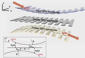
Figure 3. The schematic configuration of our designed tri-layered SPPs corrugated thin film coupler based on STIRAP.
Download figure:
Standard image High-resolution imageWith the geometry structure of our adiabatic following design (see figure 3), we set the geometry parameters as a = 40 μm, d = 50 μm, h = 30 μm, R = 45 mm, dmin = 2 μm, device length as L = 4 mm and distance between two maximum coupling point δ = 1.5 mm. We choose parameters as a, d, h (the corrugated thin films parameters), because of the consistency with the previous work in [21], to make sure that corrugated thin film waveguide can easily fabricate. Furthermore, Based on the theory of STIRAP, the key point is to generate two smooth Gaussian-shaped coupling strengths, which requires the SPPs propagate enough distance in the waveguides. As a result, we choose these geometrical parameters (L, R, δ, and dmin) to fit the two coupling strengths (between the input and middle waveguides C12 = C21 ; between the middle and output waveguides C23 = C32) as two Gaussian profiles. In our configuration with these parameters, we can obtain the corresponding Gaussian-shaped coupling strengths as shown in figure 4(a). Therefore, we can produce the complete transfer intensity of SPPs from input to output waveguide, conducted with theory of STIRAP.
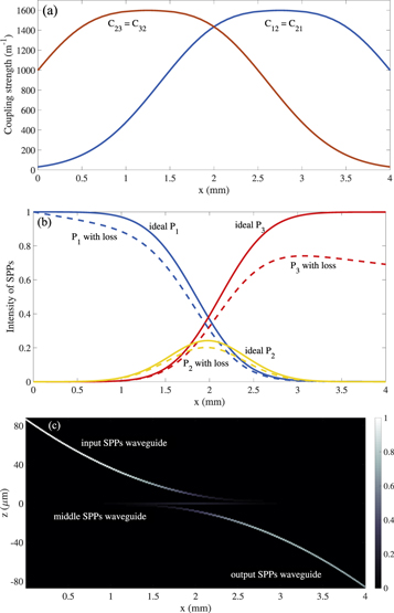
Figure 4. In this example, we give the geometry parameters as a = 40 μm, d = 50 μm, h = 30 μm, R = 45 mm, dmin = 2 μm, L = 4 mm and δ = 1.5 mm. (a) The coupling strengths between input and middle Ω2 = C12 = C21 with blue line (middle and output Ω2 = C23 = C32 with red line). (b) The intensity of SPPs on the first, middle and third corrugated thin film waveguide along with the propagation direction. (c) The visualizing simulation of SPPs propagating complete transfer from first(input) to third(output) waveguide.
Download figure:
Standard image High-resolution imageAt the beginning of the transition, the coupling strength of input and middle layer C12 = C21 is much larger than coupling strength of output and middle layer C23 = C32. Eventually, the coupling strength C12 = C21 is much smaller than C23 = C32. Thus, the whole transition is the quintessential STIRAP transition. The evolution intensities of SPPs within input (P1), middle (P2) and output (P3) waveguides are shown in figure 4(b). From the result of figure 4(b), it is conspicuously to acquire that energy has been completely transfered from input to output waveguide in the ideal case (without loss, shown with solid line). In our lossy model, we take the exponential decay along with SPPs propagation within the SPPs waveguides. However, there is some loss during SPPs propagation within the corrugated thin film coupler, which is settled as 8 dB cm–1 in this paper [18]. Therefore, the results of SPPs intensity transition with loss are shown with dashed line in figure 4(b). We still can achieve efficient transfer of intensity above 70%. The corresponding visualized results with population transfer and geometry structure is demonstrated in figure 4(c). This intuitionistic outcome illustrates that the SPPs propagate within our adiabatic device, with geometry structure of input, middle, output SPPs waveguides.
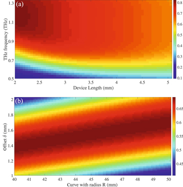
To authenticate the robustness (by varying against input frequency of THz wave and geometry parameters) of our adiabatic following design, we lay out the contour plot of final population at the output SPPs waveguide, by scanning the frequency of input THz wave (from 0.5 to 1.3 THz) and device length (from 2 to 5 mm), shown as figure 5(a). We conclude that our design can suffer broadband frequency of input THz waves (roughly from 0.9 to 1.3 THz) and larger perturbation of device length do not deteriorate our performance, which can endure length from 2 to 4 mm (energy transfer rate larger than 0.6, even in considering the loss). Furthermore, we set the device length L = 4 mm and frequency of THz wave at 1 THz, by plotting the final intensity of SPPs in output waveguide with varying the offset between two centers of curve δ (from 1 to 2 mm) and curve with radius R (from 40 to 50 mm) in the figure 5(b). It is very easy to observe that even though our device has relative large range on the geometry structure parameters (δ and R), intensity of SPPs of output waveguide still relatively maintain at good performance. Therefore, our adiabatic device is also robust against geometrical structure parameters and fabrication of our device. As the result, our design can achieve low-cost device and high fidelity device without high precision processing of manufacture. Furthermore, the robustness will remain valid if these parameters are varied and we have already illustrated our device is robust against perturbations of geometrical parameters, shown in figure 5. If we change the parameters of corrugated thin film, the mode profile of SPPs in waveguides definitely will change. Therefore, the coupling strengths of input/output and middle waveguides also will change, based on CMT. It results that the coupling strengths function along with device length will also vary. However, in our paper, we have already demonstrated that our device conforms to STIRAP. Conducted with the theory of STRIAP [25, 26] , the performance of our device maintains acceptable fidelity when the coupling functions have the fluctuations.
Figure 5. We set up the geometry parameters as a = 40 μm, d = 50 μm, h = 30 μm. (a) The robustness of our adiabatic device, by varying against frequency of input THz wave and device length. (b) Varying the offset between two centers of curve δ (from 1 to 2 mm) and curve with radius R (from 40 to 50 mm), with setting device length L = 4 mm and exciting by 1 THz wave.
Download figure:
Standard image High-resolution image
In the lossy cases, the transfer efficiency of our device maybe not remarkable. The limitation comes from two aspects. One is the higher loss of SPPs in THz waveguides, comparing with the graphene SPPs waveguide coupler working at optical light region [24]. Typically, the propagation length of graphene SPPs can reach dozens of wavelength [34], which is slightly longer comparing with propagation length of SPPs in THz corrugated thin films structure (tens or dozens of wavelength [18]). Therefore, the final transition rate of THz SPPs is limited due to the high loss. Besides, due to the adiabatic condition, the coupling strengths need smooth variation. Therefore, the length of our device requires much longer dimension than the parallel configurations [18, 21], which results in the increased damping loss of SPPs. But our device sacrifices the transfer efficiency for the duple performance of broadband and robustness, which is difficult to achieve in the parallel configurations. Secondly, these geometrical parameters in our paper are non-optimized. If the parameters are optimized, the robustness may be enhanced, but that is not the key point of this paper. Our goal is to verify the validity of STIRAP in designing a broadband and robust plasmonic coupler working at THz region, which has been successfully demonstrated (see figures 5(a) and (b)) in our work. Even though the geometrical parameters are non-optimized, our device can still achieve complete (good enough) transfer intensity of SPPs, which reflects that our device has good tolerance of the fluctuations of geometrical parameters. This is also an evidence that our design can much reduce the cost of fabrication and enhance the versatility of integrated THz devices. In the future work, we can try to realize the optimization of the parameters, and also will consider the shortcut of adiabatic (STA) [35, 36] of STIRAP to the design of SPPs waveguide coupler, to further reduce the length of the device and further increase the fidelity of the device. Whereas, if we employ the STA technique to design the SPPs waveguide coupler, it results in more complicated coupling strengths and more complex geometrical structure, which requires more investigation. But we believe that it will be the outlook to improve the performance of our design in future.
At the last of this section, we propose a possible manufacturing strategy to fabricate our designed device. The fabrication techniques of multi-layered or 3D metamaterials have been widely reported. The two crucial issues in fabricating the coupler we designed involve in (i) how to pattern the metallic corrugated films and (ii) how to stack the curved waveguides. The optional methods for the former processing are prevalent shadow mask lithography, soft lithography or nanoimprint lithography [37–39], and all techniques can guarantee the high-resolution in sub-microscale. As for the assembly, we can choose the suitable flexible polymer as the substrate, and peel off the structure after every metallic layer is transferred. Since our coupler can work in wide band, its outstanding superiority is the high tolerance for the structural imperfection induced by the fabrication.
4. Conclusion
Based on stimulated raman adiabatic passage (STIRAP) quantum control technique, we have proposed a novel coupler using a tri-layered SPPs waveguide curved configuration, in which SPPs can be completely transferred from the input to the output waveguide in the THz regime. We demonstrate that our design realizes highly efficient transfer with strong robustness against the perturbations of geometry parameters, and also illustrate that our device has good performance at broadband excited THz waves. This finding will make contribute to develop compact and robust integrated THz devices, which will promote the future applications in all-optical network and THz communications.
Acknowledgments
This work is acknowledged for funding National Science and Technology Major Project (grant no: 2017ZX02101007-003); National Natural Science Foundation of China (grant no: 61565004; 61665001; 61965005). Natural Science Foundation of Guangxi Province (grant no: 2017GXNSFBA198116, 2018GXNSFAA281163) and the Science and Technology Program of Guangxi Province (grant no: 2018AD19058). WH is acknowledged for funding from Guangxi oversea 100 talent project; WZ is acknowledged for funding from Guangxi distinguished expert project and JH is acknowledged for funding from Guangxi Bagui scholar project.