


Abstract
Topological nodal semimetal (TNS), characterized by its touching conduction and valence bands, is a newly discovered state of quantum matter which exhibits various exotic physical phenomena. Recently, a new type of TNS called topological nodal line semimetal (TNLS) is predicted where its conduction and valence band form a degenerate one-dimension line which is further protected by its crystal symmetry. In this work, we systematically investigated the bulk and surface electronic structure of the non-symmorphic, TNLS in InBi (which is also a type II Dirac semimetal) with strong spin–orbit coupling by using angle resolved photoemission spectroscopy. By tracking the crossing points of the bulk bands at the Brillouin zone boundary, we discovered the nodal-line feature along the  direction, in agreement with the ab initio calculations and confirmed it to be a new compound in the TNLS family. Our discovery provides a new material platform for the study of these exotic topological quantum phases and paves the way for possible future applications.
Export citation and abstract BibTeX RIS

Original content from this work may be used under the terms of the Creative Commons Attribution 3.0 licence. Any further distribution of this work must maintain attribution to the author(s) and the title of the work, journal citation and DOI.
1. Introduction
1.1. Topological nodal semimetal (TNS)
TNS is a newly discovered gapless-type quantum material with numerous intriguing physical properties [1, 2]. The first kind of TNS is where the conduction and the valence band touch in zero-dimension forming either quadruply degenerate points (topological Dirac semimetal) [3–6] or pairs of doubly degenerate points with opposite chirality (topological Weyl semimetal) [7, 8]. Apart from being protected due to the topological nature, these points have bands disperse through them linearly in three-dimensional (3D) momentum space, which brings interesting phenomena such as unusually high carrier mobility [9, 10], large intrinsic spin Hall effect [11], giant diamagnetism [12], and chiral anomaly in magnetoresistance [13, 14]. Recent experimental works have successfully demonstrated the existence of 3D Dirac point in materials e.g. Na3Bi [5, 15, 16], Cd3As2 [4, 17, 18], ZrTe5 [19–21], etc, while the Weyl semimetal phase is also confirmed in materials such as TaAs [6, 13, 22–26], NbAs [25–27], NbP [10, 24–26], TaP [24, 26, 28], MoTe2 [29–32], TaIrTe4 [33–35], etc.
1.2. Topological nodal line semimetal (TNLS)
If the linear touching of the bands extend from (Dirac or Weyl) points to one-dimension (1D) lines, the TNLS emerges [1]. Comparing to discrete degenerate nodes, 1D nodal line (NL) structure forms a more significant feature in the electronic band structure (figure 1(a)) and can have stronger contribution to the physically observable properties of these materials. To realize the NL phase, there are several paths including the band inversion of opposite parity bands that occurs at the high symmetry point without spin–orbit coupling (SOC) [2], inversion symmetry and TR consequence without SOC [36], mirror symmetry and TR consequence without SOC [37, 38], and mirror symmetry and TR with SOC [39]. However, as there is no guarantee that the NL will lie non-dispersively at equal energy, let alone at fermi level even if those discrete symmetries are imposed [1], observing the NL is a challenging task for experiment.

Figure 1. Schematic of two different nodal semimetals and general characterizations of InBi. (a) Dirac point and Dirac nodal line schematic showing a linear dispersion near the vicinity of the nodal line/point. (b) Ab initio calculation of InBi for several high symmetry directions shows Dirac nodal line feature indicated by red lines on RXR and AMA with contribution from Bi  In
In  and Bi
  emphasized showing a type-II Dirac point along
  direction. Brillouin zone of InBi showing the position of the nodal line in red line. (c) Simple tetragonal crystal structure of InBi showing preferred cleaving layers which is (001) plane. (d) Picture of uncleaved InBi sample and XRD data for high symmetry orientations showing a high quality sample which is consistent with the simple tetragonal structure. (e) Core level of InBi with peaks from each element indicated. (f) Wide map ARPES data of InBi showing a four symmetry feature agreeing the simple tetragonal surface brillouin zone of (001) plane.
Download figure:
Standard image High-resolution imageWhile several compounds have been predicted to be TNLS (e.g. Cu3PdN [36], Ca3P2 [40], 3D graphene network [41], and hyperhoneycomb lattice [42]), only few observations have been attempted, such as in PbTaSe2, PtSn4, and ZrSiS. Among them, PbTaSe2 is inversion asymmetric and hosts nodal loops protected by reflection symmetry under SOC [39]; PtSn4 has broken nodal-arcs but its topological character is still under investigation [43]. Furthermore, it is not easy to identify the nodal-lines in PbTaSe2 and PtSn4 convincingly due to the complicated Fermi surface (FS) of the two compounds. More recently, non-symmorphic compounds have been predicted to host nodal-line structure which are robust against the SOC due to the protection of the non-symmorphic symmetry as reported on the non-symmorphic ZrSiS family compounds where the NLs along two paths along the Brillouin zone (BZ) boundary were observed [44].
In this work, we explored the electronic structure of another non-symmorphic compound InBi and demonstrated it as a new member compound of TNLS. By using angle resolved photoemission spectroscopy (ARPES) we demonstrate that InBi possesses quadruply degenerate bands along the high symmetry lines of  (X–R–X) directions (as shown in red line figure 1(b)). The band structure and the nodal-line position show good consistency with the ab initio calculation and proved InBi as a TNLS. As the spin–orbit coupling strength is large due to the presence of heavy Bi element, our observation of the TNLS phase in this compound further proves the protection of the non-symmorphic symmetry.
2. Ab initio calculation and sample characterization
2.1. Non trivial topology in InBi
Our ab initio calculation as shown in figure 1(b) demonstrates how each band evolves with contribution from Bi  (blue color) to Bi
  (green color) emphasized. A closer investigation reveals that the bands involved in the crossing along the
  direction exchanges orbital (Bi
  to Bi
to Bi  and In
  and vice versa) and is not gapped when SOC is included, establishing InBi to possess a type-II Dirac point (see appendix A), similar to that in AMgBi (A = K, Rb, Cs) compounds [45]. Its non trivial topology was also confirmed by the evolution of the Wannier charge centers, which is using non-Abelian Berry connection [46, 47]. In addition to that, there are also quadruply degenerates NLs along XRX and AMA direction which are formed due to the glide symmetry and the screw axis symmetry intrinsic to the crystal structure of InBi (see appendix B). Since the signature Dirac semimetal has been attempted in several studies mentioned before, in this work we then focus on these topologically trivial degenerate lines along XRX (check the BZ in figure 1(b)) to demonstrate the NL and its dispersion in energy.
2.2. Sample characterizations
InBi is known to have a simple tetragonal structure [48]. As shown in figure 1(c), the crystal has a layered structure in general with cleaving plane along the [001] direction due to its relatively weak bonding between the neighboring sublayer of Bismuth [49]. Our 3D XRD results (figure 1(d)) confirm the crystal structure (P4/nmm space group) with high quality (lattice constant a = 5.014 ± 0.002 Å and c = 4.784 ± 0.003 Å). After cleaving, flat and shiny (001) surface is exposed, making it suitable for ARPES measurement (figure 1(d)). The core level photoemission spectra in figure 1(e) reveals characteristic 4d5/2 and 4d3/2 peaks for In and 5d5/2 and 5d3/2 peaks for Bi, further confirming the elemental composition of the sample. The broad FS map obtained by ARPES measurements in figure 1(f) shows the square BZ with four-fold symmetry, proving the tetragonal crystal structure and (001) cleavage plane.
3. ARPES results
3.1. FSs and high symmetry cuts
We then systematically studied the 3D band structure of InBi as illustrated in figure 2(a) where both the FS and the band dispersions along high symmetry directions are shown. The overall electronic structures appear more complex than the ab initio calculation of the bulk bands in figure 1(b), indicating that many bands have surface origin. We thus performed slab calculations for both bulk and surface electronic states (see appendix C.2 for detailed description) and plot them along the side of each corresponding measurement (e.g.  in figures 2(b)–(d), respectively). The comparisons between experiment and calculations now show nice agreement, confirming the important contribution of surface states in the photoemission intensity of InBi. In figure 2(e), the equal energy contours of the electronic structures (from the 3D ARPES data in figure 2(a)) and their evolution also shows the significance of the surface states, which again in excellent consistency with our ab initio calculation in figure 2(f).

Figure 2. General ARPES results for high symmetry cuts, equal energy surfaces, and calculated surface states (SS). (a) General 3D reconstruction of InBi ARPES data at 65 eV photon energy with several high symmetry cuts shown. (b)–(d) High symmetry cut  ARPES data with calculated SS shown which agree well. (e) Several equal energy slices of 65 eV photon energy ARPES data.
Download figure:
Standard image High-resolution imageThe existence of the surface states may prevent us from observing the crossing of the bulk bands (and thus the line-node) clearly. For example, a closer investigation on the calculated surface state at  on higher binding energy reveals several surface states band crossings sitting within the energy range (Eb = 0.71–1.26 eV), making it more difficult to resolve the bulk NLs along XRX as predicted in figure 1(b).
3.2. Photon dependence measurement
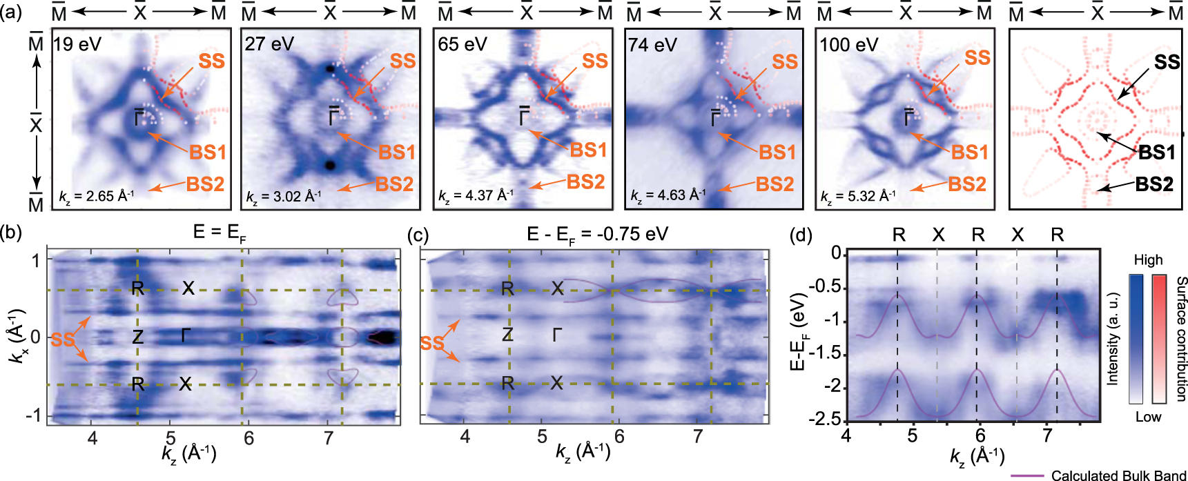
To distinguish the contribution of the bulk bands from the complex surface states, we performed photon energy dependent measurement (30–240 eV) on the electronic structure of InBi. From the FS measured at different photon energies (figure 3(a)), we could always identify a 'flower' shape feature near the  point (labeled with SS), indicating it is originated from the surface states which is further proved by our ab initio calculations. In addition, some other features on the FS, including the circular pocket around
  (labeled with BS1) and the 'bridge' shape at FS along
  (labeled with BS2) change in the shape and intensity at different photon energies, suggesting their bulk nature. We further prove the surface and bulk nature of different bands by showing the constant energy contours at FS and
  on the
  plane
plane  in figures 3(b) and (c). This was done by taking a photon energy dependence data for each photon energy probes different
  position. From the constant energy maps, we could identify two straight lines in the middle of
  and
and  These two lines come from the 'flower' shape in figure 3(a) and the lack of kz variation proves their surface nature. In contrast, the feature around
  (corresponding to the 'bridge' shape in figure 3(a)) shows strong variation with different kz value and agree nicely with the calculation result of the bulk bands (see the schematic on top of figure 3(b)), proving its bulk nature. The band structure along the XRX line also show a visible periodicity following the calculated result in figure 3(d).

Figure 3. Fermi surfaces at various photon energies and perpendicular momentum equal energy data, and Dirac point at XGM plane. (a) Fermi surfaces of InBi at different photon energies to indicate the surface state (SS) and the bulk states (BS1 for the circular shape in the middle and BS2 for the bridge shape). The calculated surface states on fermi surface are also shown for comparison. (b) and (c) Fermi surface data and equal energy surface at higher binding energy (0.75 eV) respectively along the GXRZ plane confirm surface state and bulk state features along  direction which relatively disappear at higher photon energy (kz > 5 Å−1). The calculated BS are overlapped to indicate the bulk contribution. (d) ARPES data along XRX line showing the nodal line feature as predicted by the overlapped calculation.
Download figure:
Standard image High-resolution image3.3. Dirac NL in InBi
In figure 4(a), we show detailed 3D band structures at 100 eV photon energy, where the surface states are greatly suppressed and better cross section was observed for the bulk band [50]. As shown by the ab initio calculations, a (2D) Dirac point formed by the bulk band is seen (figures 4(a) and (b)), and the calculated band structures can be nicely overlapped on top of the ARPES data.
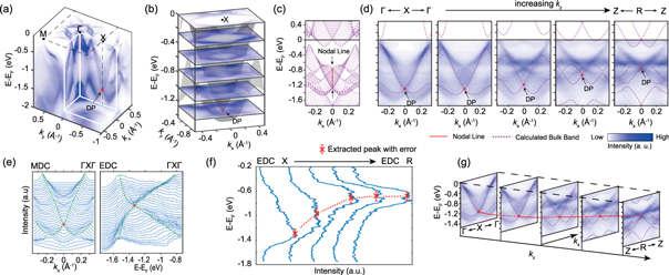
Figure 4. Demonstration of nodal line in InBi and comparison with calculation. (a) Reconstructed ARPES data from 100 eV photon energy which passes through X point with cut showing the position of Dirac point. (b) Illustration of Dirac point at X from 100 eV photon energy with ARPES data and calculated BS overlapped to each other. (c) Calculated bandstructure from  to
to  overlapped. (d) Several
  cuts at different
  position with the calculated bandstructure overlapped to demonstrate the movement of the Dirac point at different photon energy (
 position). (e) EDC and MDC at
  cut to demonstrate gapless crossing. (f) EDC from X to R showing how the extracted peak (indicating Dirac point) with error move creating the nodal line. The
  broadening makes each cut shows a broadened peak showing the contribution from neighboring
  (g) Reconstruction of nodal Line from the ARPES data.
Download figure:
Standard image High-resolution imageWe then study the evolution of the Dirac point in energy along the NL (along the XRX direction). Figure 4(d) shows cuts at different  positions (from
  to
to  ) while the results from calculation (
 to
to  ) are overlapped at figure 4(c). From each cut in figure 4(d), we observe band crossing with fair agreement with the bulk calculation indicating the existence of Dirac point for each cut, hence NL for XRX. However, the
  broadening and the increasing scattering rate at high binding energy make it harder to pin the Dirac point for each cut [51]. Thus, from the cut at
  the momentum distribution curve (MDC) and energy distribution curve (EDC) are plot at figure 4(e) to demonstrate that the crossing is indeed gapless (within our resolution). Afterwards, figure 4(f) demonstrates the EDC X through R from the cuts given in figure 4(d) which shows how the extracted peak with fitting error (indicating the Dirac point) moves creating the NL. It can also be seen that the
  broadening effect severely broaden the EDC e.g. the second EDC from the left shows a relatively broad peak due to the contribution from the neighboring
  positions. However, there is a fair agreement in the shape of the NL between the overlapped calculated result (figure 4(g)) with peaks movement of the measured ARPES cut which broadly demonstrates how the NL dispersing.
4. Summary
In summary, we have clearly demonstrated the existence of NL in non-trivial Topological Semimetal InBi which sits on the XRX line in momentum space. Remarkably, with strong SOC in InBi, the persistence of the NL demonstrates the robust protection from the non-symmorphic symmetry of the crystal structure. The discovery of InBi as a new compound of the TNLS also provides new material opportunities for the study of these exotic topological quantum phases and possible future applications.
Acknowledgments
YLC acknowledges the support of the EPSRC Platform Grant (Grant No.EP/M020517/1) and CAS-Shanghai Science Research Center, Grant No: CAS-SSRC-YH-2015-01). CF acknowledges the financial support by the ERC Advanced Grant (No. 291472 'Idea Heusler'). Advanced Light Source is operated by Office of Basic Energy Science of US DOE (contract DE-AC02-05CH11231). CCH and JJ acknowledges the support of the NRF, Korea through the SRC center for Topological Matter (No. 2011-0030787), SAE acknowledges the support from Indonesian Endowment Fund for Education (LPDP) Scholarship. SSRL is operated by the US DOE Office of Basic Energy Science.
Appendix A.: Type-II Dirac point in InBi
InBi hosts a protected type-II Dirac point which lies along the  line. In type-II Dirac point, the Dirac cone is tilted (violating the Lorentz invariant) until the equal energy surface at the Dirac point level has a hole pocket and an electron pocket apart from the Dirac point itself (figure A1). This crossing is formed by two bands with characteristic mostly from Bi
  and Bi
  and In
  where they are inverted and is not gapped after the inclusion of spin–orbit coupling. establishing InBi as a topological semimetal [45].

Figure A1. Type-II Dirac point in InBi. (a) Reconstruction of type-II Dirac point on  plane showing a Dirac cone that violates Lorentz invariant. (b) Equal energy surface at the Dirac point energy contains hole pocket, electron pocket, and the Dirac point itself as the transition point.
Download figure:
Standard image High-resolution image
Appendix B.: Symmetry protection in InBi
Within P4/nmm space group, there are two symmetries governing InBi that will give the protection. First is the glide symmetry with  plane as glide mirror which can be expressed with the operator below
and the screw axis symmetry  followed by translation which is given as below (take
  )
)
With the given operators, we can obtain the following expression

and

When those operators act on high symmetry line of XRX for  and XRX and MAM for
  there is a degenerate line analogous to Kramers' degeneracy since the
  [52]. Thus, this crystal symmetry gives protection to NLs in InBi as long as the structure is preserved.
Appendix C.: Material synthesis and experimental methods
C.1. Sample synthesis
Single crystals of InBi were grown by a modified horizontal Bridgman technique. In and Bi were mixed at a molar ratio of 1:1. The mixture was sealed in an evacuated quartz tube, pre-reacted by heating until it completely melted. Using the obtained ingot, the crystal growth was carried out in a homebuilt horizontal moving tube furnace. The heating unit was kept at 200 °C, and moved in a lateral direction of the sealed quartz tube with a speed of 1 mm h−1. The obtained single crystals had good cleavage along the ab-plane (001), producing flat surfaces of ∼1 × 1 cm2. The in-plane resistivity, measured by the four-probe method, was very low (<500 nΩ cm) for T < 10 K and the residual resistivity ratio (2 K versus 300 K) was over 300, indicating a high quality of the crystals.
C.2. Angle resolved photoemission spectroscopy
ARPES measurement were performed at i05 Diamond Light Source and at BL 5-4 Stanford Synchrotron Radiation Lightsource both equipped with Scienta R4000 analyzers. The sample temperature and the pressure during measurement were 10 K and lower than 1.5 × 10⁻¹⁰ Torr, respectively. The angle resolution was 0.2° and the overall energy resolutions were 15 meV. The samples were cleaved in situ along the (001) plane.
Tunable soft x-ray from synchrotron light source ranged from 30 to 240 eV is used to get the complete band structure image along the  and
and  directions and also to distinguish the bulk and the surface band structure contribution [50]. The electron momentum parallel to the surface can be calculated from the relation
 and
and  where
where  is the mass of free electron,
  is the kinetic energy of electron outside of the material,
  is the polar angle,
  is the azimuthal angle,
  is the momentum parallel to the material with
  and
and  are the components of it along the
  and
and  directions. Even though the perpendicular momentum is not conserved, the perpendicular momentum inside the material can be predicted with the relation
  with
with  as the inner potential for the material and
  as the effective mass of the electron [53]. The more complete explanation of ARPES technique can be found in other publications [54–57].
C.3. Ab initio calculations
The bulk band calculation was performed by using density-functional theory (DFT) with the projected augmented wave potential as implemented in the Vienna ab initio simulation package [58, 59] with spin–orbit coupling calculation included, generalized gradient approximation [60] exchange-correlation functional employed. The maximally localized Wannier functions [61] constructed from DFT were used to calculate bulk 2D FSs with a dense k-point grid.
The surface state associated with (001) surface were calculated by first reconfirming that the cleaving plane terminates in between the Bismuth layer which showed formation energy approximately 1.3 eV per unit cell lower than other possible planes. Then, a slab model with a 36-atomic-layer structure was applied. The top and bottom surfaces were both terminated by Bi, and a vacuum layer of over 20 Å was added in z direction to avoid the coupling between top and bottom surfaces. The weighted wave function contributions from the outermost tri-layer (3-atomic-layer) are shown in color gradation (100% in red to 0% in white) in order to distinguish the surface states contribution from bulk states (of 36 atomic layers) contribution. The force convergence criterion of 0.01 eV Å−1 was adopted for structural optimization.