


Abstract
We use polarization resolved micro-photoluminescence to analyze the dipolar nature of single core/shell cadmium selenide/cadmium sulfide (CdSe/CdS) dot-in-rods. Polarization analysis, anisotropy measurements on more than 400 nanoparticles, and defocused imaging suggest that these nanoparticles behave as linear dipoles. The same methods were also used to determine the three-dimensional orientation of the emission dipole, which proved to be consistent with the hypothesis of a linear dipole tilted with respect to the rod axis. Moreover, we observe that for high-energy pumping, the excitation transition of the dot-in-rod cannot be approximated by a single linear dipole, contrary to the emission transition.
Export citation and abstract BibTeX RIS

Content from this work may be used under the terms of the Creative Commons Attribution 3.0 licence. Any further distribution of this work must maintain attribution to the author(s) and the title of the work, journal citation and DOI.
1. Introduction
Development in the chemical synthesis of high-quality and low-blinking colloidal quantum dots [1–3] has been driven by their potential as single photon sources [4, 5]. Inorganic semiconductor nanocrystals with a core/shell architecture, namely, two materials assembled in a concentric topology and with a straddling alignment of the energy band gaps, display very good fluorescence properties and high quantum efficiency at room temperature [6]. In particular, colloidal core/shell dot-in-rods made up of a spherical dot of cadmium selenide (CdSe) embedded in a rod-like cadmium sulfide (CdS) shell have been the subject of intense research activity, with particular emphasis on the dependence of optical properties such as lifetime [7], absorption anisotropy [8], and biexciton generation [9, 10] on the rod aspect ratio and shell thickness [9]. These nanoemitters have demonstrated high absorption and a good photostability at room temperature, together with a quantum yield estimated as high as  [9, 11] and a high degree of linear polarization of the emitted light [12, 13]. Moreover, due to their elongated shape, they have the unique property of lying with the long axis parallel to the surface, which is an advantage when one wants to control the orientation of the elongated axis [12]. This geometry means it may be possible to deterministically control the orientation of the quantum dot dipole, which is highly important to optimize the coupling of polarized nanoemitters to photonic [14, 15] or plasmonic structures [16]. For this purpose, the determination of the orientation of the emitting dipole associated with a dot-in-rod is crucial, since this may not necessarily lie along the long axis of the rod.
Different types of emitting dipoles can be distinguished depending on their geometry, the most simple being a linear, or one-dimensional (1D) dipole. However, in many cases such as some molecules [17], single nitrogen-vacancy in diamond [18], and some semiconductor quantum dots [19–22], the emission originates from two degenerate states with orthogonal dipole orientations. The emission corresponds then to an incoherent sum of two orthogonal 1D dipoles and is referred to as a 'two-dimensional (2D) dipole.' The 1D or 2D dipole nature of a given nanoemitter is related to the energy level structure and must be known for the orientation of a single nanoemitter to be extracted from polarization measurements.
In this paper, we perform polarimetric measurements on CdSe/CdS dot-in-rods, whose chemical synthesis is described in [12, 23]. Using the theoretical model developed in [19], we suggest that these emitters behave as linear dipoles, and we determine the orientation of the emitting dipole by analyzing the emission polarization. A statistical analysis of the polarization anisotropy measurements supported by defocused imaging suggests that the emission dipole of dot-in-rods is tilted with respect to the dot-in-rod axis. Finally, we perform a polarimetric analysis of the dipole excitation field, highlighting that at high energies the excitation dipole is not fully polarized.
After a brief summary of the synthesis method (section 2), we determine the in-plane and out-of-plane orientations of a single dipole from the measured degree of linear polarization in section 3. In section four, a larger ensemble measurement of the polarization anisotropy of more than 400 dot-in-rods is used to confirm the obtained results, also consistent with the defocused imaging analysis described in section 5. We then study how intensity fluctuations affect the polarization of the dipole transition, suggesting that the polarization is not correlated to the local charge fluctuations (section 6). In the last section, a polarimetric analysis on the dot-in-rods' excitation dipole at high energy levels is also presented.
2. CdSe/CdS dot-in-rods synthesis
Two different specimens of CdSe/CdS dot-in-rods, hereafter respectively referred to as DR1 and DR2, are studied. Both present characteristic core/shell morphology and, particularly in this instance, a round particle of CdSe is embedded within a rod-like shell of CdS, as illustrated in figure 1(a). The samples DR1 and DR2 have been synthesized following the seeded-growth approach described in [12] with a few modifications (see the

Figure 1. (a) Sketch of the synthesized dot-in-rod, made up of a spherical CdSe core embedded in a rod-like CdS shell. (b) Absorbance (solid) and photoluminescence (dashed) spectra of samples DR1 (blue) and DR2 (red), respectively. (c), (d) Transmission electron microscope (TEM) images of sample DR1 (l = 58 nm, d = 2.7 nm, t = 7 nm) and DR2 (l = 72 nm, d = 2.9 nm, t = 4 nm), respectively.
Download figure:
Standard image High-resolution imageLow-magnification transmission electron microscopy (TEM) analysis was performed using a Jeol JEM-1011 electron microscope operating at 100 kV, equipped with a charge-coupled-device (CCD) camera. TEM samples are prepared by drop-casting dilute nanocrystal solutions onto carbon coated copper grids. Diluted concentrations of a nanocrystal solution  were used to prevent the formation of bundles of vertically stacked dot-in-rods when drop-cast onto a substrate. The moderate particle concentration increases the spacing between nanocrystals and diminishes the likelihood of Van der Waals interactions between the long alkyl chains surrounding each nanocrystal. The nanocrystal length (
 50 nm) is expected to favour a dot-in-rod orientation with the long axis lying parallel to the surface. After drop casting, we have measured, by atomic force microscopy (AFM) and TEM (see, e.g., figures 1(c) and (d)), the rod dimensions as l = 58 nm, d = 2.7 nm, t = 7 nm and l = 72 nm, d = 2.9 nm, t = 4 nm for the DR1 and DR2 samples, respectively, where l and d are the nanoparticle length and width, and t is the nanoparticle height on the surface. We therefore find, as expected, that the dot-in-rods are lying horizontally on the substrate employed for optical observation (a glass substrate of root mean square roughness less than 1 nm as measured by AFM), as also shown in the TEM images (see figures 1(c) and (d)).
3. Polarization analysis on a single dot-in-rod
In this section, a polarimetric analysis on samples DR1 and DR2 is presented, and the theoretical framework developed in [19] is used to extract the orientation (Θ,Φ) of a single nano-emitter.
As mentioned in the introduction, the question of whether a class of emitters behaves as a linear (1D) dipole must be addressed before turning to orientation measurements. In our case, as the dot-in-rod nanostructures present anisotropic shells, the radiating dipole, associated to the dot-in-rod crystallographic structure, may have its emission influenced by the high index rod, inducing a higher local field in the direction of the rod. Distinguishing an effect of the high index rod is beyond the scope of this paper: as it is customary in the literature [8, 13, 25], we discuss only the emission of the (dot + rod) structure as a whole, as it is the only quantity to which we have experimental access. In order to determine whether the dot-in-rods behave as 1D dipoles, we will compare their measured emission polarization with the theoretical behaviour of a 1D dipole, as explained below.
The origin of the spherical polar coordinates is chosen to be the core centre, and the z direction corresponds to the optical axis of light detection. In the case of a linear dipole, the orientation of the vector  is indexed by an out-of-plane angle Θ and an in-plane angle Φ, as illustrated in figure 2(a) (top panel). Note that for a 2D dipole (bottom panel), the angles (Θ,Φ) will refer to the normal of the plane formed by the two orthogonal dipoles.
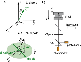
Figure 2. (a) Orientation of a dipole in a (x,y,z) system. A 1D dipole (top panel) sits along  oriented at (Θ,Φ) angles. For a 2D dipole (bottom panel), the angles (Θ,Φ) refer to the orientation of the normal to the dipoles plane. (b) Schematic of the set-up used to measure the dipole emitted intensity while rotating the half-wave plate. The emission is collected by an oil-immersion objective. The z direction corresponds to the objective optical axis. A polarizing beam splitter cube splits the beam according to polarization, and the signal is recorded by two avalanche photodiodes.
Download figure:
Standard image High-resolution imageIn a prior experiment, we used a Hanbury Brown and Twiss (HBT) set-up (using a non-polarizing beamsplitter) to verify that, at the used deposition concentration, most of the particles were well isolated from each other and emitted single photons. An experimental coincidence histogram is illustrated in figure 3(a). The g2 peak at zero delay is close to zero, leading us to the conclusion that the dot-in-rods of this study are indeed single photon sources [24].
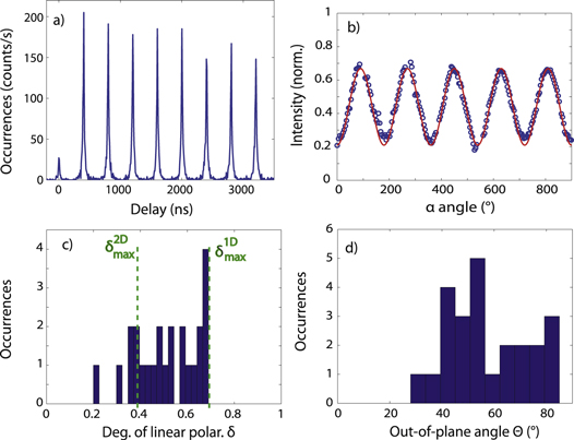
Figure 3. (a) Coincidences histogram obtained for a dot-in-rod with a laser repetition rate of 2.5 MHz with the HBT set-up. (b) Circles: detected intensity as a function of polarization analysis angle α for a single DR2 dot-in-rod. Solid red line: fitting of experimental curve with equation (1). The fitted value of δ for this particular dot-in-rod equals 52  . (c) Histogram of experimental values of δ measured on 24 single DR2 dot-in-rods covered with 50 nm of PMMA. (d) Histogram of experimental values of Θ, deduced using the data in figure 4, connecting δ to Θ for a 1D dipole for 24 single DR2 dot-in-rods.
Download figure:
Standard image High-resolution imageLet us now describe the polarization analysis set-up in detail. The sample consists of spin-coated dot-in-rods on a glass coverslip of refractive index 1.5 and covered with 50 nm polymethyl methacrylate (PMMA, refractive index 1.5) to protect the emitters from the environment. The signal emitted by a single dot-in-rod was collected by an oil-immersion objective of numerical aperture (NA) 1.4, mounted on an fluorescence confocal microscope. A schematic representation of the optical path is reported in figure 2(b). A half-wave plate was placed in the emission beam path and rotated by an angle  . A polarizing beam splitter cube was positioned in front of the photodiodes in order to separate the emission in x and y polarizations. The rotating half-wave plate together with the polarizing beam splitter acts like a polarizer, rotating the polarization axis by an angle α. This experimental configuration allows the two orthogonal polarizations to be measured, using two different avalanche photodiodes. It is then possible to normalize the detected intensity on each photodiode by the total signal and avoid errors due to fluctuations of the total intensity.
Figure 3(b) displays a representative photoluminescence signal detected from an isolated DR2 dot-in-rod by the avalanche photodiode x and normalized to the total emitted intensity recorded by both photodiodes. On each photodiode, the detected intensity oscillates between minimum value Imin and maximum value Imax as the half-wave plate is rotated.
As calculated in [19], the detected photoluminescence signal from a 1D or a 2D dipole as a function of the rotating angle α follows the relation:

where Imin and Imax stand for the minimum and maximum detected intensity. In the case of a 1D dipole,  , since the detected intensity is maximum when the axis of polarization α is aligned with the 'bright axis' of the dipole, referred to as Φ. For a 2D dipole,
  . The detected intensity is minimum when the axis of polarization α is equal to Φ.
The phase of the measured modulation curve can be used to obtain Φ, provided that the 1D or 2D nature is known (e.g.,  for the data presented in figure 3(b)). Moreover, the amplitude of this modulation, characterized by the degree of linear polarization δ, allows the out-of-plane orientation Θ of the dipole to be determined [19].
From the experimental curve, one extracts the factor δ, defined as:

In figure 4 the simulated curves calculated for both 1D and 2D dipoles show the theoretical dependence of δ on the out-of-plane angle Θ of the dipole. The model uses the experimental values of the NA (1.4), the refractive indices of glass and PMMA (1.5), and the distance e between the emitter and the air–PMMA top surface. The spin-coated layer of PMMA is 50 nm thick, so we have assumed that e = 50 nm (see figure 2(b)).
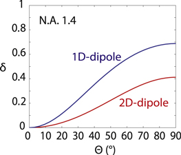
Figure 4. Calculated values of δ as a function of out-of-plane angle Θ for 1D (blue) and 2D (red) dipoles located at 50 nm from the air–PMMA dielectric interface and detected using an oil-immersion objective with NA=1.4.
Download figure:
Standard image High-resolution imageAs displayed in figure 4, the correspondence between the degree of linear polarization δ and the out-of-plane angle Θ depends on the 1D or 2D nature of the dipole. The case  corresponds either to a vertical 1D dipole or to a vertical 2D dipole (two horizontal dipoles), which in both cases presents a rotational symmetry configuration about the z-axis. Therefore, for Θ = 0
 , the degree of polarization δ is zero in both cases. It increases with Θ up to a maximum value which depends on the 1D or 2D nature of the dipole, the NA of the objective, and the presence of a dielectric interface. The maximum value of the degree of linear polarization δ, obtained for
  , is higher for a 1D dipole than for a 2D dipole (here, respectively, 70
  and 40
  for a dipole located at 50 nm from the air–PMMA interface and a NA = 1.4), showing that the emission is less polarized for the 2D dipole, as it is a sum of two incoherent dipoles. It is worth noting that, in this configuration, even a perfect 1D dipole will not lead to
  . The unique relationship between Θ and δ allows the orientation of a given dipole to be extracted by measuring the degree of linear polarization, given that it is known whether it has a 1D or 2D dipole nature. Here we apply this method on dot-in-rods in order to determine both their nature and orientation.
Relation (1) between the intensity detected and the polarization angle α was used to fit the experimental curve (red continuous line in figure 3(a)). The fit is very satisfactory, leading to δ = 0.52 with an uncertainty of 0.05. The same polarization measurement was performed on more than 20 dot-in-rods, whose results are displayed in figure 3(c).
The histogram of experimental δ shows values mostly larger than 0.4 and up to 0.7. According to the simulated curves of δ as a function of Θ reported in figure 4, δ is always smaller than 0.4 in the case of a 2D dipole, whereas it can reach 0.7 in the case of a 1D dipole. Most of the values of δ measured on these 24 DR2 dot-in-rods are therefore incompatible with a 2D dipole. On the other hand, all these values are compatible with the hypothesis of a homogeneous ensemble of linear dipoles. Similar results have been reported on semiconductor nanorods [25], and the fine-structure model for semiconductor nanorods developed in [26] and pseudopotential calculations for CdSe rods [27] predict that the emission transition polarization is almost 100% linear.
The experimental determination of δ, using the theoretical curve (reported in figure 4) calculated for a 1D dipole, leads to values of the out-of-plane angle Θ ranging from 30°–85°. This indicates that most of the dipoles are not horizontal. However, as indicated by our TEM analysis as well as by an AFM investigation performed on spin-coated nanorods [28], such elongated dot-in-rods show a tendency to lie horizontally on the substrate. The measured values of Θ let us suggest that the axis of the emitting dipole does not match the horizontal elongated axis of the dot-in-rod. Control experiments with the shorter DR1 sample (having the same core as DR2) have also been performed. The resulting values of Θ were in the same range (25°−80°), also proving that DR1 dipoles are not horizontal. This similar distribution of dipole out-of-plane angles for dot-in-rods having different ratios indicates that the shell length is not the determining factor of the dipole orientation. This conclusion is consistent with the fact that the states involved in the emission are localized in the CdSe core, which is the same in both cases.
In figure 5(a), we sketched the orientation of a 1D dipole associated with a dot-in-rod compared to the elongated axis of the dot-in-rod. The dipole has been located in the dot position. The angle between the dipole and the dot-in-rod has been labelled as β. It is worth mentioning that the plane defined by the dot-in-rod and the dipole axes is most likely tilted from the vertical plane by an angle labeled γ (in purple in figure 5(a)). Therefore, the angle Θ equals  only for γ = 0 and
  in general.
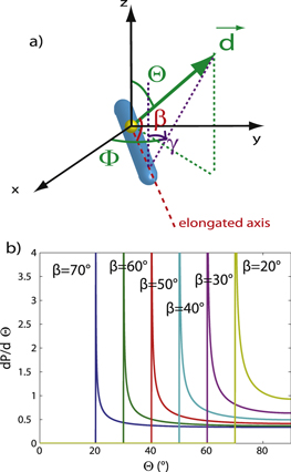
Figure 5. (a) Orientation of the emitting dipole compared to the dot-in-rod orientation. The angle between the dipole and the elongated axis is β. (b) Calculated probability density  for β angles set from
  –
– .
.
Download figure:
Standard image High-resolution imageIn order to extract information on β from the histogram of measured Θ angles in figure 3(d), one can establish the relation between the angles Θ, γ, and β:

For a given β, assuming a uniform distribution of γ between  and
and  (
( ), we find the theoretical distribution of Θ:

In figure 5(b), we display the probability density  of Θ for different values of β from
  –
– . A maximum is reached for each curve at
  , with no possible value of Θ below
  (as it is clear from figure 5(a)).
We find no occurrence for Θ angles lower than  and a peak between
  –
– . As we did not measure any Θ angles lower than
  , we conclude that no dot-in-rods presents a value of β higher than
  . Moreover, the occurrences of Θ are higher for Θ values between
  –
– . This fact is a good indication that most of the β angles should take a range of values between
  –
– .
.
In figure 6, we overlay the histogram of measured Θ angles and the histograms of Θ values calculated from equation (3), assuming Gaussian distributions of angles β centered at  ,
,  , and
, and  , respectively, (see inset), with a full width at half maximum (FWHM) of
  .
.
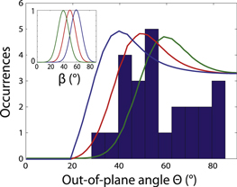
Figure 6. Histogram of experimental values of Θ, as displayed in figure 3(d). The red (respectively, green and blue) curve stands for the simulated distribution of Θ corresponding to a Gaussian distribution of β centered at  (respectively,
  and
and  ) with a FWHM of
  (inset).
Download figure:
Standard image High-resolution imageThe fair correspondence observed in figure 6 between the measured and the simulated histograms of Θ, assuming a distribution of β centered at  with a FWHM of
  , indicates that the angles β between the dipole and the dot-in-rod axis are expected to lie between
  –
– .
.
4. Polarization analysis on a larger statistics of dot-in-rods
In this section, we support the previous results with a polarization analysis on a larger ensemble of dot-in-rods. We use an alternative method, proposed by Chung et al [20], to confirm the linear nature and orientation of the dot-in-rods' dipole. The set-up is presented in figure 7(a). The x- and y-polarized emission of the same emitters is imaged simultaneously on two CCD cameras situated after a polarizing beam splitter cube. This polarizing beam splitter cube has been placed between the microscope and the CCD detector. The optical beam is reasonably well collimated on arrival at the CCD detectors so that the theoretical model of [19] can be used. It is thus possible to obtain for each nanoemitter the experimental value of the polarization anisotropy A, defined as :

with Ix (respectively Iy ) representing the value of the measured intensity of a given emitter on the CCD camera x (respectively y).
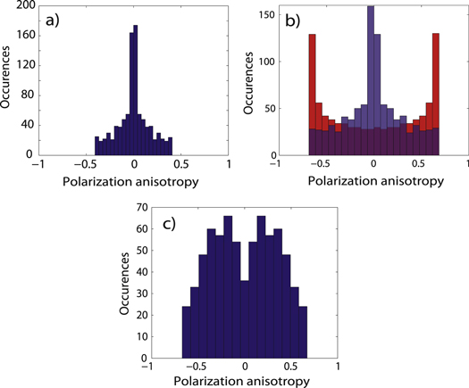
Figure 8. (a) Calculated polarization anisotropy A for a collection of randomly oriented 2D dipoles, emitting at λ = 600 nm, covered by a layer of PMMA and located at 50 nm from the air interface. (b) Calculated polarization anisotropy histograms (same experimental conditions as in (a)) for a collection of 1D dipoles randomly oriented (blue) and horizontally lying ( ) on the substrate (red). (c) Calculated polarization anisotropy histograms for a collection of 1D dipoles with Θ distributed according to the histogram in figure 3(d).
Download figure:
Standard image High-resolution imageWe measured the anisotropy polarization A on a collection of several hundreds of dot-in-rods. In figure 7(b), we report the experimental histogram of polarization anisotropy for 413 DR2 dot-in-rods.
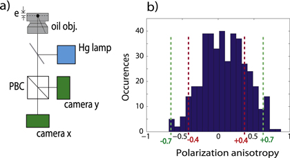
Figure 7. (a) Schematic of the polarization anisotropy measurement set-up. The sample, with emitters deposited on a planar substrate and protected by a 50 nm thick layer of PMMA, was excited by means of Hg lamp and observed with an oil-immersion objective. A polarizing beam splitter cube is placed in front of two CCD cameras in order to image x and y polarization separately. (b) Distribution of anisotropy measurements A of 413 DR2 dot-in-rods embedded into a 50 nm thick film of PMMA.
Download figure:
Standard image High-resolution imageAs detailed in [19], for any value of Θ, it is not possible to measure A higher than 0.7 for a 1D dipole and 0.4 for a 2D dipole. Therefore, the experimental histogram of polarization anisotropy allows the 1D or 2D nature of a collection of dipoles to be determined. Figure 8(a) displays the distribution of A for a collection of 2D dipoles. If the dot-in-rods were 2D dipoles, the associated histogram of polarization anisotropy would not reach values higher than 0.4. The fact that the experimental histogram displays A values higher than 0.4 and up to 0.7 implies that the dot-in-rods are mostly 1D dipoles. This result is consistent with the earlier reported polarization analysis. In figure 8(b), we plot both histograms for 1D dipoles corresponding respectively to an isotropic distribution of Θ (in blue) and to a collection of horizontal dipoles ( ) on the surface (in red). None of these two histograms match the experimental data shown in figure 7(b). This indicates that the dipoles' orientations are neither horizontal nor completely isotropically distributed on the substrate.
In order to refine the description of the dipoles' orientation to achieve better agreement with our experimental observations, we choose a distribution of Θ based on the experimental histogram in figure 3(d), where Θ was shown to be distributed between  –
– , with more occurrences around
  and
and  . Therefore, we simulate in figure 8(c) a histogram of polarization anisotropy corresponding to 720 1D dipoles with Θ values fixed at
  (90 dipoles),
  (180 dipoles),
  (180 dipoles),
  (90 dipoles),
  (90 dipoles), and
  (90 dipoles), representing a distribution of out-of-plane angles Θ close to that measured in figure 3(d). The relative polarization histogram is reasonably similar to the experimental histogram of polarization anisotropy in figure 7(b). This result is in good agreement with the values of Θ established in section 3, and it supports the conclusion that the dipole is not aligned with the geometrical dot-in-rod axis.
The emitting dipole and its orientation could be first inferred by the crystallographic structure of the dot-in-rod. Moreover, the anisotropic CdS shell shape and its high dielectric constant could act as an antenna and influence the dipole orientation. In any case, in this experiment, the polarimetric analysis of the emission provides information on the orientation of the resulting dipole. This result can also be compared with those from [29], where the authors reported that, due to a permanent density of surface-charges, the crystallographic axis of a dot-in-rod, and therefore its internal electric polarization, can lie at a significant angle with respect to its elongated axis [29]. In this case, the induced electric field may modify the dipole orientation.
In the following section, we use a defocused imaging technique to further support the conclusion that the dipoles are not parallel with the substrate.
5. Defocused imaging
Defocused microscopy is a successful imaging technique [13, 30, 31] which allows the emission pattern of a dipole to be probed by moving the focal plane away from the sample by a distance as large as 1 μm (the vertical focusing length is  . Each defocused image provides information about the orientation of a given dipole. The defocused images acquired on 30 DR1 dot-in-rods are reported in figure 9. It is evident that only a few of these patterns have met the symmetry that could be expected if the dipoles were lying horizontally. However, quantitative derivation of the orientation angles is a delicate procedure. The precise measurement of the orientation of a dipole close to an interface by analysis of a defocused image requires non-trivial calculations. These calculations must take into account the emission in near field to fit the images and to properly extract quantitative information. We have instead chosen to compare the collected images with those simulated by Patra et al [32], which were calculated for similar observation conditions.
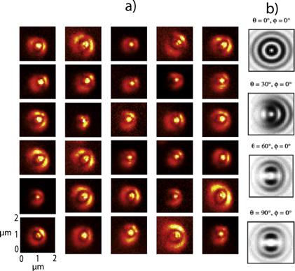
Figure 9. (a) Defocused images (area size: 2 x 2 μm2) with δz = 1 μm of 30 different DR1 dot-in-rods observed through an oil-immersion objective of NA = 1.4. (b) Theoretical defocused images for Θ corresponding to  ,
,  ,
,  , and
, and  , respectively (reproduced from Patra et al in [32]), considering an oil-immersion objective of NA = 1.2 at a distance δz = 1.2 μm from the sample. The white colour represents the lower intensity zones.
Download figure:
Standard image High-resolution imageFrom that theoretical reference, the rotational symmetry of the defocused pattern corresponds to a horizontal dipole (Θ =  ). In contrast, when the dipole is standing up on the substrate (Θ =
  ), the defocused image consists of concentric circles. In the intermediate situations where the dipole is tilted on the surface, the defocused image presents only one axis of symmetry. Our experimental defocused images display such a single axis of symmetry. We can thus qualitatively conclude that most of the dipoles are tilted on the surface. Moreover, none of them is standing up on the substrate. (Perfect concentric circles would be expected.)
The various results from the degree of linear polarization measurement, the polarization anisotropy analysis, and the defocused microscopy images consistently suggest that the measured value of δ is due to an angle β between the dot-in-rod axis and its associated dipole.
6. Dipole transition
The different analysis methods reported in the preceding sections all suggest that the dipole transition corresponding to the total emission of a CdSe/CdS dot-in-rod is 1D, in agreement with theoretical reports [26], and that the dipole orientation differs from the rod long axis. However, it has been demonstrated that dot-in-rod luminescence fluctuates between dark, intermediate, and bright states, giving rise to an overall emission instability [9]. Such events have been widely discussed in the literature and were recently assigned to different nanoparticle charged states [9, 33, 34]. The dark state is most likely due to a charging of the particle by trapping of a charge carrier in its shell. When the particle is charged, Auger-assisted non-radiative recombination (rate  ) competes with radiative recombination (rate
  ), leading to dark (

 ) and intermediate (
 ∼
∼  ) states. In order to characterize and observe the intensity fluctuations of a single dot-in-rod, we report in figure 10(a) the photoluminescence intensity time trace of one single DR2 dot-in-rod in the detection configuration shown in figure 2(b), excited by a 450 nm pulsed laser. The emission exhibits different photoluminescence intensity levels corresponding to bright, intermediate, and dark states. We divided the photoluminescence intensity in several intensity ranges, as displayed by the dotted lines, and plot in figure 10(b) the decay curves accumulated during the periods corresponding to the different intensity ranges defined in (a). The lifetime
  is then different, depending on the considered intensity range, as observed on CdSe/zinc sulfide (ZnS) nanocrystals in [35].

Figure 10. (a) Photoluminescence intensity time trace of a single DR2 dot-in-rod. Intensity counts have been separated (dotted line) into different levels to isolate bright and intermediate emission levels. (b) Emission decay curves analyzed separately for the different photoluminescence count ranges defined in (a). The lifetime is longer for the bright state (15–20 kHz) than for intermediate levels because of the fast non-radiative transitions.
Download figure:
Standard image High-resolution imageFor the bright state, the decay curve can be fitted by a mono-exponential curve with a well-defined lifetime (70 ns as measured in figure 10(b) for intensities in the 15–20 MHz range). The presence of an additional fluctuating  rate in the intermediate states appears as a faster non-exponential decay.
In order to determine if dipole transitions with different orientations are involved in the different emission states of the dipole, figure 11 reports the normalized intensity (blue continuous line) detected from the single DR2 dot-in-rod studied in figure 10(a). The interruption of the curve corresponds to dark states, seen from comparison with the emission curve in figure 10(a). A polarization degree  is found. We introduce a threshold of intensity set to 8000 counts s−1. One can therefore consider separately the intermediate level (defined as intensity below 8000 counts s−1) and the bright state (emitted intensity above 8000 counts s−1) and distinguish their response to polarization measurements. The red circles correspond to the signal recorded when the intensity is above the threshold. The green circles represent the signal corresponding to the intensity below the threshold.
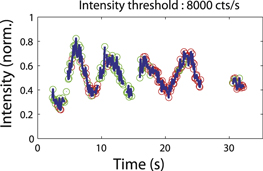
Figure 11. Detected normalized photoluminescence time trace from a single dot-in-rod while rotating the polarization analysis (speed: 15 ). The blue line corresponds to the total detected signal. The green (red) circles correspond to emission with intensity below (above) an intensity threshold fixed at Ith = 8000 counts s−1.
Download figure:
Standard image High-resolution imageIn figure 11, we note that the normalized intensity curves are superimposable in terms of amplitude and phase for the emitted signal below and above the threshold of intensity. The degree of linear polarization  remains the same for any intensity on both sides of the threshold. For a dozen single dot-in-rods the same observation was found, confirming the reproducibility of this behaviour. This result indicates that the polarization of the energy level for the charged emitter is the same as for the neutral emitter, letting us suggest that the polarization of a single dot-in-rod is not modified by the presence of non-radiative recombination channels.
7. Polarization analysis of the excitation
We consider in this section the result of polarimetric measurements of the excitation dipole. The nature (1D or 2D dipole) and orientation of excited and emitting dipoles are not necessarily the same, since they involve different transitions in the case where non-resonant excitation is used.
The polarization of the 450 nm excitation was fixed by setting a polarizer cube and a half-wave plate along the excitation path. The half-wave plate was continuously rotated with an angle  , and the photoluminescence intensity was measured on both photodiodes. A representative photoluminescence signal as a function of the angle α, detected from an isolated DR, is displayed in figure 12(a). In the same way as for emission, we define the excitation degree of linear polarization as δexc = (
 ). In the case of the data in figure 12(a), we measure
  3000 counts s−1 and
  8000 counts s−1. The signal, in this case of the polarization analysis of the excitation, is more sensitive to the dot-in-rod total intensity fluctuations, since it cannot be normalized. The experimental degrees of polarization δexc measured on 16 single DR1 particles are summarized in the histogram on figure 12(b): δexc lies in the range [0.4;0.8].

Figure 12. (a) Detected intensity emitted by a single DR1 dot-in-rod as a function of polarization excitation angle α. (b) Histogram of experimental values of δexc for 16 DR1 dot-in-rods covered with a 50 nm thick PMMA layer.
Download figure:
Standard image High-resolution image
The theoretical modelling and interpretation of an excitation polarimetric curve are not the same as those obtained for polarimetric emission analysis (under non-polarized excitation). The orientation of the electric field  of the excitation laser at the position of the emitter is very close to the orientation
  defined by the polarizer in the excitation beam path (even when taking into account any effects of the high numerical aperture objective), as demonstrated in [36]. Therefore, for a 1D dipole
  , one can write the intensity
  of the emission signal as [19, 36]:

It follows that, for an orientation (Θexc, Φexc) of the excited dipole,  . It turns out that a δexc equal to unity is expected for any out-of-plane orientation Θexc. Measuring the emission polarization dependence on the excitation polarization is therefore not an effective way to measure the in-plane and out-of-plane orientation of the emitting dipole [37]. The fact that we measure values of δexc much lower than unity in figure 12(b), however, indicates that the dot-in-rod cannot be considered equivalent to a linear dipole under excitation, at least for the excitation wavelength used in this work. Given that CdSe/CdS dot-in-rods are large polarizable systems (high dielectric constant), the local field is lower along the rod axis for a fixed value of an applied electric field. The anisotropic response of the rod may then modify the excitation polarization.
Moreover, the excitation degree of polarization has been found to be lower than unity also for CdSe nanorods [38] and semiconductor nanowires [39, 40]. In [41], the excitation polarization anisotropy of core/shell CdSe/CdS rod-in-rods at a collective scale in solution has been proven to be lower when excited far above the band edge, as is the case for our 450 nm excitation. For CdSe/CdS spherical quantum dots, we measure no polarization dependence for the excitation (not plotted here). This observation can also be explained by the structure of the higher excited energy levels, which forms a continuum of energy levels with different polarization states.
Conclusion
We have performed various polarimetric measurements on single core-shell CdSe/CdS dot-in-rods in order to determine the orientation of their emission and excitation dipole. We have found, on a collection of single nanoparticles, that the emitting dipole can be considered as a linear dipole tilted from the elongated dot-in-rod axis. These results were confirmed by the defocused imaging technique. In addition, whenever the emitters are in the bright or in an intermediate charged state, the emission polarization properties do not change. This suggests that fluctuations in the non-radiative decay channels of the dot-in-rod do not modify the polarization direction of the radiative transition. Finally, through polarized excitation, we show that, when excited at high energy, the dot-in-rods' excitation dipoles cannot be modeled as simple 1D dipoles. This study shows that dot-in-rods are promising room temperature polarized single photon sources.
Acknowledgements
The authors acknowledge Francis Breton, Dominique Demaille, and Willy de Marcillac for their technical support; Catherine Schwob, Paul Bénalloul, Jean-Marc Frigerio, Stefano Vezzoli, Mathieu Manceau, Godefroy Leménager, and Paola Atkinson for fruitful discussions. The authors thank the Agence Nationale de la Recherche (P3N Delight and JCJC Ponimi) and the Centre de Compétence NanoSciences Ile-de-France (CʼNano IdF, Sophopol, NanoPlasmAA) for funding this work.
Appendix
Dot-in-rod synthesis. All synthesis steps are carried out in an inert atmosphere of N2.
Cd and S stock solution. 0.060 g of CdO (cadmium oxide 99.99% Sigma-Aldrich), 1.000 g of TOPO (trioctylphosphine oxide 99% STREM), 0.285 g of ODPA (octadecylphosphonic acid 99% Polycarbon Industries), and 0.080 g of HPA (hexylphosphonic acid 99% Polycarbon Industries) are allowed to combine at  under vacuum. After 1 h under vacuum, the brown-coloured solution is exposed to a constant flow of
  and heated to
  until it becomes colourless and transparent. At this point, 1.5 g of TOP is injected, and the heating supply is definitely removed. When the sample reaches room temperature, a solution containing 0.120 g of S (sulfur 99.998% Sigma-Aldrich) dissolved in 1.5 g of TOP (trioctylphosphine 99% STREM) is injected into the flask. At room temperature, any chemical reaction between S and Cd is hampered. This colourless solution is finally stored in an inert environment.
CdSe nanodot synthesis. In brief, 3.700 g of TOPO, 0.280 g of ODPA, and 0.060 g of CdO are stirred in a 50 mL flask, heated to 150  , and exposed to vacuum for 1 h. Afterwards, the solution is heated to 300
  while flushing the flask with
  until it turns transparent and colourless. At this stage, 1.5 g of TOP is injected into the reaction batch, and the temperature is set to 370
  before injection of a Se-based solution (selenium powder 100 mesh 99.5
  Sigma-Aldrich). After the temperature is stabilized to the set value, the Se-TOP solution (0.063 g Se + 0.575 g TOP) is swiftly injected, and the growth is allowed to proceed for 1 min before removing the heating mantle. The CdSe nanodot solution is then transferred into a drybox and twice purified by sequential precipitation and re-solubilization with methanol and anhydrous chloroform, respectively. Finally, the nanodots are dissolved in TOP in a final CdSe dot concentration of 7.5 μM. The as-described CdSe nanodots showed a band-edge absorption peak at 536 nm.
CdSe/CdS DRs synthesis. In a typical synthesis step, 0.085 g of CdO, 3.000 g of TOPO, 0.285 g of ODPA, and 0.080 g of HPA are combined. The mixture is pumped to vacuum (50 mTorr) for 1 h at 150  and then, after transferring to a
  atmosphere, heated to 350
  . At this point, 1.5 g of TOP is injected. After the temperature has newly re-set to 350
  , a solution of S precursor-TOP-CdSe nanodots is swiftly injected into the flask. This solution is prepared by dissolving 0.120 g of S in 1.5 g of TOP and adding 100 μl of a solution of TOP-dissolved CdSe dots (see above). After the injection, each CdSe/CdS nanocrystal solution is allowed to grow, respectively, for 8 min in the case of nanorods DR2 and 15 min for DR1. In the latter case, after 15 min of growth time, a Cd and S stock solution (see above) is dropwise injected (rate = 300 μl min−1, syringe volume = 12 ml) at the fixed temperature for an additional 30 min. The synthesis reactions are stopped by removing the heating source. When the solution temperature cools down, the nanoparticles are transferred into a N2-supplied drybox and twice purified by precipitation with anhydrous methanol and re-solubilization in anhydrous chloroform. All samples are stored in the drybox until optical and morphological investigations are conducted.