


Abstract
We report on thickness-dependent cation ordering and ferroelectric properties of (001)-oriented epitaxial PbSc0.5Ta0.5O3 (PST) thin films grown by pulsed laser deposition on SrTiO3 (001) and Si (001) substrates. The PST film thickness was varied from 30 to 200 nm. Only films thicker than 40 nm reveal (partial) cation ordering, which increases with thickness as confirmed by the appearance and intensity of superstructure reflections in x-ray diffraction and transmission electron microscopy. In accordance with the two-state thermodynamic model, temperature-dependent dielectric constant investigations showed the presence of two kinds of phase transitions belonging to the normal ferroelectric and the relaxor state, respectively, both being present in the PST films. The influence of cation ordering on the phase transition and ferroelectric properties is discussed in detail.
Export citation and abstract BibTeX RIS

Content from this work may be used under the terms of the Creative Commons Attribution 3.0 licence. Any further distribution of this work must maintain attribution to the author(s) and the title of the work, journal citation and DOI.
1. Introduction
Even though relaxor ferroelectrics were first studied in Russia in the 1960s [1], the understanding of these systems is still insufficient [2]. Relaxor ferroelectrics have recently attracted considerable interest due to their extraordinary frequency-dependent dielectric and piezoelectric properties which make them potential candidates for technological applications such as multilayer capacitors, tunable filters, sensors, actuators, infrared detectors and electro-optic devices [3–5]. Despite having potential for these numerous applications, relaxors are still challenging and puzzling materials due to their inhomogeneous nature on the mesoscopic scale [6, 7]. In contrast to normal ferroelectrics the physical properties of which can be adequately explained by the Ginzburg–Landau–Devonshire theory, relaxor ferroelectrics exhibit a diffuse dielectric anomaly near the dielectric maximum with significant frequency dispersion. This dielectric maximum does not signify any macroscopic structural phase transition. The relaxor nature of these materials is a manifestation of either (i) a quenched random electric field developing due to impurities, lead vacancies or chemical and lattice disorder, or (ii) the existence of polar nanoregions (PNRs) in the highly polarizable host lattice well above the temperature of the dielectric maximum [8]. Understanding the role of these two contributions in these materials is quite intriguing as well as very intricate. The contribution of the former mechanism to the relaxor nature is quite well known [9–11], but recent experimental studies have provided sufficient proof of the existence of PNRs well above the temperature of the dielectric maximum [12–14].
PbSc0.5Ta0.5O3 (PST) is well known as a ferroelectric relaxor which crystallizes in the perovskite structure, and with the general formula A (B'B'O3). In PST, A sites are occupied by Pb2+ cations and B sites are equally shared by Sc3+ and Ta+5 cations [15, 16]. In the case of B-site disordered PST, Sc3+ and Ta5+ atoms are statistically distributed on the B-sites of the cubic perovskite lattice. In the ordered structure, Sc3+ and Ta5+ cations occupy the B-sites alternatively in the 〈111〉 direction, which leads to superstructure reflections with a double unit cell [17]. In PST, the large ionic radius difference (13%) between Sc3+ (0.0885 nm) and Ta5+ (0.078 nm) offers a very good chance for the material to be completely ordered. However, due to the charge difference of two between the B-site cations, PST is nevertheless on the border between the ordered and disordered arrangements of Sc3+ and Ta5+ cations. Brinkman et al [10] have already shown that completely ordered films show a dielectric constant as high as bulk ceramics and it can be tuned down significantly by altering the degree of cation ordering. The Curie temperature of PST has been reported to vary between 273 and 300 K, depending on the degree of cation ordering on the B sites [18]. The degree of ordering of Sc3+ and Ta5+ cations in PST ceramics as well as in sol–gel prepared thin films can be controlled by sintering or subsequent heat treatment [10, 19, 20]. However, to our knowledge there has been no report on alteration of cation ordering and on the influence of (dis)ordering on phase transitions in thin films prepared by pulsed laser deposition (PLD).
In this work, the influence of film thickness on cation ordering and phase transitions of PST films prepared by PLD is studied. In the case of sol–gel films and bulk ceramics, perovskite phase formation takes place through diffusion by annealing the samples at high temperatures. PLD, in contrast, is a highly metastable process in which phase formation is rather a non-equilibrium and highly complex process. Thus in order to understand the mechanism of cation ordering in PLD-prepared films, both reduction in thickness and annealing strategies were tested.
2. Experimental
Epitaxial PST (001) thin films were deposited on vicinal SrTiO3 (STO) (001) and on Si (001) substrates by ablating a stoichiometric PST target with KrF excimer laser pulses (wavelength 248 nm, pulse duration 20 ns). Prior to the deposition, commercial STO substrates (CrysTec GmbH, Berlin) were chemically treated with a buffered HF solution and annealed in air at a temperature of 1000 °C in order to achieve TiO2-terminated surfaces with unit-cell high step-terrace structures [21]. The Si(001) substrates were cleaned ultrasonically with acetone, methanol and deionized water for 5 min without any further acid treatment. In this paper the following three types of heterostructures on STO and Si substrates with different thicknesses are considered:
- (PST/LSMO): STO(001)/La0.7Sr0.3MnO3 (001)/PST (001).
- (PST/SRO): STO(001)/SrRuO3 (001)/PST (001).
- (PST/Si): Si (001)/ZrO2:Y2O3 (001)/CeO2 (001)/LaNiO3 (001)/PST (001).
Here, these types of structures will be designated as PST/LSMO, PST/SRO and PST/Si, respectively. The structural (lattice parameter and space group for the bulk) properties of the materials used in this study along with the deposition temperature are tabulated in table 1 [22–29]. All the films discussed in this paper are epitaxial and the different growth conditions used for the fabrication of these heterostructures are published elsewhere [30–33]. The PST film thickness was varied from 30 to 200 nm. All heterostructures were deposited in situ, i.e. without interruption of the vacuum, and were cooled down in an oxygen atmosphere to room temperature (RT) with a slow cooling rate of 5 K min−1. To facilitate the macroscopic electrical measurements, Pt top electrodes with 60 × 60 μm2 area were sputtered by radio frequency sputtering at RT through a shadow mask.
Table 1. Tabulated values of the space group, lattice parameter and growth temperature for the different materials used.
| Material | Space group | Lattice parameter (Å) | Substrate temperature (°C) |
|---|---|---|---|
| PST [22] | For ordered:  ; for disordered : ; for disordered :  |
For ordered: a=b=c=8.136; for disordered: a=b=c=4.068 | 550 |
| SRO [23] | Pbnm | a=5.563,b=5.530,c=7.844; for pseudo-cubic (a=b=c=3.910) | 700 |
| LNO [24] |  |
a=5.457,c=13.14; for pseudo-cubic (a=b=c=3.861) | 650 |
| LSMO [25] |  |
a=5.508, c=13.361; for pseudo-cubic (a=b=c=3.876) | 650 |
| CeO2[26] | Fm3m | a=b=c=5.410 | 700 |
| YSZ [27] | Fm3m | a=b=c=5.148 | 700 |
| Si [28] | Fd3m | a=b=c=5.419 | Substrate |
| STO [29] | Pm3m | a=b=c=3.901 | Substrate |
Crystallographic characterization was performed using a Philips X'Pert MRD x-ray diffractometer with Cu Kα (λ = 0.15 418 nm) radiation. Cross-section and plane-view samples for transmission electron microscopy (TEM) were prepared by mechanical thinning followed by Ar ion-beam milling. Conventional and high-resolution TEM (HRTEM) studies were performed on a Philips CM20 T microscope at 200 kV and on a Jeol 4010 at 400 kV, respectively. The surface morphology and local switching polarization response were investigated using a commercial atomic force microscope (XE-100, Park Systems, Suwon) in the piezoresponse force microscopy mode. Polarization–voltage (P–V) hysteresis loop and switching current–voltage (I–V) characteristics of the PST films were recorded by means of a ferroelectric tester (AixACCT 2000, Aachen). Dielectric constants were calculated from the capacitance measured using a Hewlett Packard 4194A impedance analyzer. The temperature-dependent dielectric constant measurements were performed by placing the sample inside a Lake Shore cryogenic probe station, with open liquid nitrogen circulation, operating in the temperature range of 70–350 K using wire bonding contacts on silver paste. For these measurements, the temperature was continuously varied with a heating rate of 1 K min−1.
3. Results and discussion
Out-of-plane (θ–2θ) and in-plane (ϕ) x-ray diffraction (XRD) measurements (not shown here) revealed that all heterostructures were grown epitaxially, with PST in the pure perovskite phase. In the case of samples of type PST/Si, in-plane measurements showed a rotation of the lattice of the PST film by an azimuthal angle of 45° with respect to the buffer layer and substrate, as discussed in [33]. No other parasitic or pyrochlore phases were observed.
In order to check the status of cation ordering in the PST films, the samples were tilted by an angle ψ = 54.7° so that the Bragg condition for the (111) planes was fulfilled. Superstructure reflections were observed for all the three heterostructures as shown in figure 1, but only for thicknesses larger than 40 nm. The presence of superstructure reflections  at around 18.8° confirms that the films are cation-ordered. The degree of cation ordering was measured in the PST films by calculating the order parameter S, which is defined as
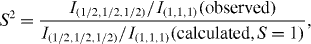
where I is the integrated intensity of the subscripted reflections. The value of the order parameter (S) for completely ordered and disordered systems corresponds to 1 and 0, respectively [10]. It should be noted that as the degree of cation ordering increases, other superstructure reflections (3/2 3/2 3/2) also become visible at around 60°. The average degrees of ordering calculated from the order parameter for the 50 nm (for PST/LSMO) and 200 nm (for PST/Si) films were found to be 30 and 70%, respectively. It has been observed that the degree of cation ordering in our PLD-prepared PST films increases with film thickness. However, below ∼ 40 nm thickness, PST films exhibit no superstructure reflections. An enhancement in cation ordering with annealing has been reported for sol–gel prepared PST films in the literature [10]. Thus to find a possibility of improving the cation ordering in disordered films, 30 nm thick PST films (of type PST/LSMO) were annealed at 550 °C in 1 bar oxygen for 5 h. However, no improvement was observed in the status of cation ordering; additionally, the films showed a pyrochlore phase on annealing at higher temperatures than 550 °C. Thus, it is quite evident that there is no room for the improvement in cation ordering by annealing at moderate temperatures, and annealing at higher temperatures deteriorates the quality of the films possibly due to lead losses and interdiffusion between the layers in PLD-prepared films.
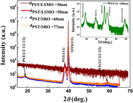
Figure 1. XRD patterns of PST samples of type PST/LSMO show that the 30 nm thick PST films are not cation ordered but the 50, 60 and 77 nm thick PST films are (partially) cation ordered. The samples were tilted by an angle ψ = 54.7° for observing the (111) planes.  superstructure reflections obtained near an angle of 18.87°. Inset: PST/Si showing superstructure reflections for a 200 nm thick PST film.
Download figure:
Standard image High-resolution imageMicroscopically, the status of cation ordering in these heterostructures was thoroughly investigated by TEM and HRTEM. The selected area electron diffraction (SAED) patterns for PST/LSMO-type heterostructures with 30 and 50 nm thick PST films captured along the [ 10] direction are shown in figures 2(a) and (c), respectively. Surprisingly, and in contrast to XRD investigations, the SAED pattern (only indexed for PST) recorded for not only the 50 nm but also the 30 nm thick PST film shows an additional set of reflections (shown by red color circles) as shown in figures 2(a) and (c). To investigate the possible origin of this additional set of reflections in SAED, cross-sectional dark field TEM images (figures 2(b)–(d)) were recorded by using one of the additional reflections. It was observed that in the case of the 30 nm thick PST film, only the LSMO layer was showing up in bright contrast, but not the PST layer, which signifies the LSMO layer as the only origin of the additional reflections in this case. However, for the 50 nm thick film, the PST layer also shows a clear bright contrast revealing that in this sample the observed additional reflections are indeed superstructure reflections of PST. Thus, these TEM observations are in agreement with our XRD results. The average size of cation-ordered nanodomains was found to be around ∼ 3 nm in the 50 nm thick film.
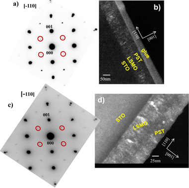
Figure 2. TEM images and SAED patterns for cross-section samples along the [ 10] direction, (a) for 30 nm and (c) 50 nm thick PST films. (Indexing of the SAED patterns for PST only.) The red color circles are highlighting the set of additional reflections obtained. (b) Cross-sectional dark field image captured using one of the encircled reflections showing no cation ordering in the 30 nm thick PST film. (d) Cross-sectional dark field image captured using one of the encircled reflections showing that the 50 nm thick PST film is (partially) cation ordered.
Download figure:
Standard image High-resolution imageSimilar to the samples of type PST/LSMO, an additional set of reflections was observed for a 200 nm thick PST film deposited on Si (PST/Si-type heterostructure), as shown by red color circles in figure 3(a). It is quite evident from the cross-sectional image captured using one of these additional reflections (figure 3(b)) that the latter are superstructure reflections, and thus the 200 nm thick PST film in the PST/Si-type heterostructure has a higher degree of cation ordering as compared to the thin films discussed for the PST/LSMO-type heterostructure. The average size of the nanodomains was found to be around ∼ 15–18 nm.
Figure 3. (a) SAED pattern for a cross-section sample along the [ 10] direction, indexed only for the 200 nm thick PST film on Si. The red color circles are highlighting the set of additional reflections obtained. (b) Cross-sectional dark field TEM image captured by using one of the encircled reflections showing a significant amount of degree of ordering.
Download figure:
Standard image High-resolution imageFor the PST/SRO-type heterostructure, two plane-view samples of 60 and 77 nm PST film thickness were investigated. Similar to PST/LSMO- and PST/Si-type structures, additional superstructure reflections were observed for the PST/SRO-type heterostructure in SAED patterns captured in the [101] pole position as shown by red circles in figures 4(a) and (c). Using one of the superstructure reflections, dark field plane-view images were recorded for both 60 and 77 nm thick PST films as shown in figures 4(b) and (d), respectively. It was observed that the domain size of cation-ordered regions increases from 5 to 10 nm as the film thickness was varied from 60 to 70 nm, respectively. Thus, it is quite evident from XRD and TEM investigations that with an increase in thickness, there is a significant enhancement in both the degree of cation ordering and the size of cation-ordered domains in PLD-prepared films.
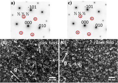
Figure 4. SAED patterns for (a) 60 nm and (c) 77 nm thick PST film for [101] poles of plane-view samples. The red colored circles highlight the set of superstructure reflections obtained. Dark field plane-view images captured using  -type reflections for (b) a 60 nm thick PST film and (d) a 77 nm thick PST film.
Download figure:
Standard image High-resolution imageIn order to explore the possibility of epitaxial strain responsible for the quenching of cation order in 30 nm thick films (of type PST/LSMO), reciprocal space mapping measurements (figures 5(a) and (b)) were performed using (103) diffraction peaks for both the 30 and 50 nm thick PST films. The change in the c/a ratio was almost the same for both the films, thus epitaxial strain as a possible reason for the quenching of cation order is still debatable. However, in comparison with the relatively thick films, thinner films are more prone to the influence of substrate clamping on cation ordering. The other possible explanation for not having cation ordering in the 30 nm thick PST film could be that the size of the cation-ordered domains is too small (∼ less than 2 nm) to be detected by XRD and TEM techniques, or—as reported in the literature—it is possibly influenced by lead vacancies present in the 30 nm thick PST film [34].
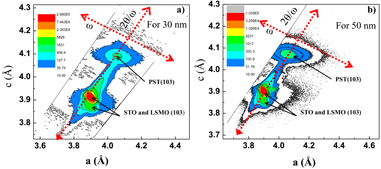
Figure 5. Reciprocal space map of the (103) reflections for (a) a 30 nm thick film, and (b) a 50 nm thick film. Both films were found to be partially strained on LSMO/STO.
Download figure:
Standard image High-resolution imageThe temperature-dependent dielectric properties of partially ordered (200 nm thick PST film within PST/Si) and disordered (30 nm thick PST film within PST/LSMO) PST films were measured by using a small ac voltage of 0.1 V (small to avoid the influence of the applied voltage on any phase transitions). During the measurements, it was found that the PST films were quite sensitive to high temperatures and thus, in order to avoid any possible change in the PST films due to heating, the dielectric constant was measured between 100 and only 350 K. Typical curves recorded for the partially ordered and disordered films for three different frequencies are shown in figures 6(a) and 7(a), respectively. In the case of relaxors, a diffuse and frequency-dependent dielectric maximum is generally expected [35], but our observed data for both the partially ordered and disordered films show a rather sharp and frequency-independent dielectric maximum accompanied by a small hump toward the lower temperature as shown in the inset of figure 6(a). The dielectric maximum for the partially ordered and disordered PST films was observed at 274 and 264 K, respectively. Likewise for the dielectric loss, sharp peaks were observed at 273 and 263 K for the partially ordered and disordered PST films, as shown in figures 6(b) and 7(b), respectively. These sharp phase transitions observed for both partially ordered and disordered PST films are quite unique as compared to reported phase transitions for PST in bulk and in films [10, 36–40].
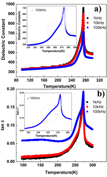
Figure 6. (a) Temperature dependence of the dielectric permittivity for a 200 nm thick PST film (of type PST/Si), recorded for three frequencies. Inset: a hump observed at lower temperature showing the presence of another phase transition. (b) Temperature dependence of dielectric loss.
Download figure:
Standard image High-resolution imagePrincipally, in bulk, for the canonical relaxors, instead of having a single microscopic phase transition, there are four different temperature regions observed, signifying different macroscopic phase transitions locally [41]. At high temperatures, there is no net dipole moment due to the thermal fluctuations, and upon cooling the sample, PNRs start to grow in size. The temperature at which PNRs appear is known as Burns temperature (Td). Further cooling helps these PNRs to grow in size and correlate with each other and this temperature is known as T* [41]. On further cooling, the PNRs keep growing until the temperature of the dielectric maximum (Tm) is reached, after which either these PNRs freeze to a non-ergodic phase at freezing temperature Tf (for canonical relaxors) with a diffuse phase transition, or to a normal ferroelectric state at Curie temperature TC.
Due to different boundary conditions as compared to bulk materials the scenario is different in the case of thin films. In thin films, there are various sources of strain such as a two-dimensional clamping effect from the substrate, thermal expansion and lattice mismatches, or local defects due to oxygen and/or lead vacancies, which can dramatically influence the order of the phase transition [42–46]. Because of strain effects, the phase transitions observed in thin films have the character of more diffuse phase transitions. Besides the strain effect, the order of the phase transition and the shape of the dielectric maximum in PST films will also be governed by the degree of cation ordering. Thus, it may be difficult to observe the characteristic for bulk relaxors' sequence of phase transitions on the temperature scale in thin films. Furthermore, it is known that even highly ordered (91%) PST films are expected to show a high frequency-dependent dielectric maximum diffuse over a temperature range of 50 K [10]. In the case of partially ordered or completely disordered PST thin films, the dielectric maximum is diffuse over more than a 100 K temperature range.
As discussed earlier, in our case one set of films was partially ordered and another was completely disordered. Thus, in principle, one has to consider the possibility that the sharp, frequency-independent dielectric maximum peak observed in both sets of films is not corresponding to the dielectric maximum of the relaxor phase. These observations indicate the presence of a different kind of phase transition in ordered and disordered PST films, which is not corresponding to the relaxor state. Along with these sharp dielectric peaks, small frequency-dependent humps were observed at the lower temperatures for both ordered and disordered films. In comparison with the partially ordered PST film, the small hump observed along with the dielectric maximum for the disordered film is more diffuse and thus is not distinguishable in the dielectric constant measurements. However, the hump is more distinct in the dielectric loss for the disordered film as shown in the inset of figure 7(b). In the case of the partially ordered PST film, the hump is unambiguous, and the dielectric maximum for it was observed around 265 K for 10 kHz. For the disordered film, the hump was 100 K broad around the temperature of 150 K. The observed features of the hump are a typical signature of a relaxor phase transition. A hypothesis regarding the existence of two separate phase transitions for homogeneously disordered and heterogeneously disordered states already has been reported in the literature for relaxor ceramics [34]. In this hypothesis, it was concluded that the homogeneously disordered state exists at higher temperatures and the heterogeneously disordered phase (consisting of randomly oriented nanodomains) exists at low temperatures. Besides that, no hump was observed for the completely disordered films. However, in contrast to the reported hypothesis, in this study we have observed the hump for both ordered and disordered films and no frequency dependence was observed for the dielectric peaks at high temperatures. Thus, we propose that these PST films are a mixture of ferroelectric and relaxor phases, where the phase transition observed at higher temperatures belongs to a ferroelectric state whereas the hump observed at lower temperatures belongs to the relaxor phase. Thus, the temperature variation of the dielectric constant confirms the two-state thermodynamic model of Kuchta and Debierre [47], which proposes the co-existence of a ferroelectric state and a relaxor state simultaneously.
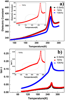
Figure 7. (a) Temperature dependence of the dielectric permittivity for a 30 nm thick PST film (of type PST/LSMO), recorded for three frequencies. Inset: a hump observed at lower temperature showing the presence of another phase transition. (b) Temperature dependence of the dielectric loss.
Download figure:
Standard image High-resolution imageMacroscopic ferroelectric properties were investigated at 100 K and RT for both 30 nm (disordered) and 50 nm (partially ordered) PST films (of type PST/LSMO) as shown in figures 8(a) and (b). At 100 K, both films behave as conventional ferroelectrics, and for the 50 nm thick film, the spontaneous polarization Ps, remnant polarization Pr and coercive voltage Vc under the application of 8 V are about 28 μC cm−2, 13 μC cm−2 and 1 V, respectively. The 30 nm thick film shows similar ferroelectric properties, although the hysteresis loops are not saturated and show leakage in one direction. At RT, both films show rather a leaky hysteresis, although switching peaks are still visible in the I–V characteristics as shown in figure 8(b). In order to improve the quality of the top electrode and for better electrical contacts between the top electrode and the subsequent layer, in situ epitaxial LSMO top electrodes were grown on PST films. The epitaxial top electrodes were patterned into 60 × 60 μm2 capacitors by a standard etching procedure. Significant improvements were observed in the hysteresis loops, and the films could be switched without further problem of leakage as shown in figure 9. This shows that even above the dielectric maximum temperature, there is still a significant amount of ferroelectric behavior in the films which is a typical relaxor ferroelectric characteristic. Pr observed was found to be 8 μC cm−2 which is two times higher than the previously reported values for electroded PST films on SRO [30–33].
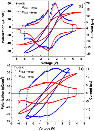
Figure 8. Macroscopic (P–V) and switching (I–V) hysteresis curves of a 30 and a 50 nm thick PST film on LSMO/STO (a) at 100 K and (b) RT.
Download figure:
Standard image High-resolution image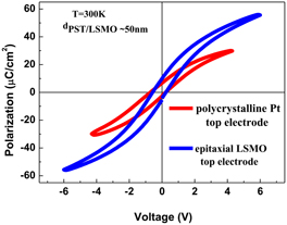
Figure 9. Macroscopic (P–V) hysteresis curves of a 50 nm thick PST film at RT for a polycrystalline Pt top electrode and for an epitaxial LSMO top electrode, respectively.
Download figure:
Standard image High-resolution image
4. Conclusions
In conclusion, epitaxial partially cation-ordered and disordered PST (001) thin films were fabricated by PLD. It was found that cation ordering and disordering are thickness-dependent phenomena in PLD-prepared thin films. As the film thickness increases, the films show a better degree of cation ordering in TEM and XRD. The size of cation-ordered domains varied between ∼ 3 and ∼ 15 nm with thickness. Temperature-dependent dielectric constant measurements revealed a diffuse phase transition corresponding to the relaxor phase at low temperatures and a sharp phase transition related to the ferroelectric phase at high temperatures for both partially ordered and disordered films. The P–V loops measured at 100 K and RT show that the films are ferroelectric. This report further emphasizes the intriguing and intricate nature of relaxor materials, and that new theories need to be developed in order to understand them comprehensively.
Acknowledgments
The authors thank Dr E P Houwman (IMS-University of Twente) for useful discussion and Mr N Schammelt for PLD system maintenance. This work was funded by DFG via SFB 762.