

Abstract
Interface trap density (Dit) in a metal oxide semiconductor (MOS) capacitor with an aluminum-doped hafnium oxide (Al:HfO2) layer is investigated using the conductance method. Three device-under-tests (DUTs) were fabricated to investigate the impact of Al concentration in HfO2 on Dit. Note that the atomic layer deposition cycle ratio of HfO2:Al2O3 for DUT A, B, and C was varied from 3:1, 5:1, and 10:1, respectively. It was observed that the extracted Dit of DUT C is 3.84 × 1013 cm−2 eV−1 (which is the lowest value in the three DUTs). In addition, the measured leakage current of DUT C is the lowest. The optimum Al concentration in Al:HfO2 would pave a new road for future CMOS technology.
Export citation and abstract BibTeX RIS
1. Introduction
Many types of high-k materials have been under investigation to look for the right option for a gate-insulation layer in metal oxide semiconductor (MOS) devices [1]. High-k material in a gate insulation layer of MOS devices can enhance the gate-to-channel capacitive coupling, so that MOS devices can gear-up with better performance as well as considerable immunity to short-channel-effect. As the prerequisite for high-k material (vs. SiO2) to be adopted as the gate insulation material for MOS device, however, its electrical property to suppress gate-leakage current in MOS device is more essential than any other characteristics.
In order to implement thermodynamically stable interface state at the oxide-semiconductor interface of MOS device, binary metal oxides including Al2O3 [2, 3], La2O3 [4, 5], ZrO2 [6, 7], TiO2 [8, 9] and HfO2 [10–12] have been studied when they form the direct/physical contact with silicon. Among them, HfO2 has been currently adopted as the high-k material in MOS devices for mass production. The cations such as Si [13, 14], Zr [15, 16], and Al [17–22] for HfO2 have received lots of attention as the promising candidate because of their cost-effectiveness. A doped HfO2 film with Al2O3 has been reported to induce the phase transformation from the m-phase to the t/c-phase with large grain sizes, which can open the window for various electrical characteristics [23]. To dope Al into HfO2 thin film (i.e. to regulate the Al content ratio in the HfO2 film), atomic layer deposition (ALD) cycles for Al2O3 with controlled cycle ratios of Al-O to Hf-O precursor were inserted in the process for HfO2. The Al cation in the film with Al2O3 will have an impact on the value of dielectric constant (k). A higher concentration of Al leads to an increase of k because of the phase transformation, but a too high Al concentration eventually decreases the value of k due to the low-k value of Al2O3 [23]. Therefore, a proper Al concentration should be designed to implement a good electrical property (i.e. high-k value and its corresponding high gate-to-channel capacitance) with a superior interface state between insulation and semiconductor for MOS device operation. Quantitative analysis of interface trap density (Dit), which is a vital parameter in electrical properties of the MOS capacitor with Al-doped HfO2, is necessary because Dit affects the device performance, threshold voltage, and carrier mobility in the channel. In this work, using conductance method, Dit values of MOS capacitor with Al-doped HfO2 are extracted.
2. Fabrication and measurement
The cross-sectional view of metal-insulator-semiconductor (MIS) capacitor used in this work is illustrated in figure 1(a). The HRTEM (high resolution transmission electron microscopy) image of the Al-doped HfO2 layer in HfO2 (4.2 nm)/SiO2 (1.3 nm)/P++-Si was shown in figure 1(b). First, a heavily doped p-type silicon substrate is prepared, and it was cleaned by the RCA cleaning process at 80 °C. Then, the native oxide on it was removed using diluted HF solution, and thereafter the substrate was rinsed in deionized water. Next, using ALD, a 4.2 nm-thick Al-doped hafnium oxide (HAO) layer was deposited on the silicon substrate [see figure 1(b)]. To investigate the impact of Al concentration in HfO2 layer, three device-under-test (i.e. DUT A, B, and C) were fabricated with three different ALD cycle ratio of HfO2:Al2O3 (i.e. 3:1, 5:1, and 10:1 for DUT A, B, and C, respectively). The precursors, i.e. Tetrakis(ethylmethylamino) hafnium (TEMAHf) and trimethylaluminum (TMA), was used to deposit HfO2 and Al2O3 layer, respectively. The growth rate (Å/cycle) of HfO2, Al2O3 was 1.3 Å/cycle, 0.9 Å/cycle, respectively. Ozone was used as oxidant, and argon gas was used as carrier gas. The chuck or stage for wafer was heated up at 340 °C. Afterwards, 80 nm-thick TiN layer was deposited onto the Al-doped HfO2 layer. Note that the 10 nm-thick TiN layer above the Al-doped HfO2 layer was first deposited by ALD (to make a good interface adhesion), and then the 70 nm-thick TiN layer was deposited by sputtering. Those metal and dielectric layers were patterned by photolithography and etching processes. Then, to crystallize the Al:HfO2 film, a rapid thermal annealing was implemented at 700 °C for 30 s in N2 ambient. The interface trap density was extracted using conductance method. Using Keithley 4200 A semiconductor characterization system, DUTs were measured.
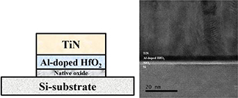
Figure 1. (a) The cross-sectional view of MIS (metal insulator semiconductor) capacitor using a HAO (Al-doped HfO2) layer. (b) The cross-sectional TEM image of Al-doped HfO2 (4.2 nm)/SiO2 (1.3 nm)/P++-Si. The active area of this capacitor is 95.8 × 95.8 μm2.
Download figure:
Standard image High-resolution image3. Results and discussion
The properties of Al:HfO2 film can be electrically evaluated with measured C-V and G-V at various gate voltages and frequencies. The quality of interface states between Al-doped HfO2 and the semiconductor in MOS capacitor can be characterized through the capacitance and its equivalent parallel conductance as functions of voltage and frequency. Using the conductance method, the interface trap density (Dit) can be experimentally extracted out. In the conductance method, the MOS capacitor is modelled with an equivalent circuit, from which the interface trap density (Dit) can be quantified. The equivalent circuit of a MOS capacitor is shown in figure 2(a) for the conductance method. The capacitive circuit network consists of oxide capacitance (Cox), semiconductor capacitance (CS), interface trap capacitance (Cit), and interface-trap-associated resistance (Rit). Using the loss mechanism due to the capture and emission process of carriers via interface traps, Dit can be extracted as a function of gate voltage and frequency. It is convenient to replace the circuit of figure 2(a) with figure 2(b) for simplifying the circuit model. The LCR meter generally assumes that the device consists of a parallel combination of Cm-Gm (see figure 2(c)). Figure 3 shows the measured C-V characteristics for each DUT at 1 MHz. With decreasing the Al concentration in HfO2 layer, it is observed that the dielectric constant of DUT C is higher than that of the others. In reality, when the Al concentration increases, the dielectric constant increases up to 43 (see table 1). Note that the dielectric constant of pure HfO2 is 20 ∼ 25. Herein, in order to extract the value of Cox, we exploit the extrapolation method for each DUT (see figure 4). The intercept on x-axis in figure 4 is matched to the accumulation capacitance. For example, the capacitance of DUT A, B, and C is 192.53 pF, 198.98 pF, and 224.03 pF, respectively. The extracted equivalent parallel conductance (GP) with various frequencies in DUT A, B and C is summarized in figure 5. From the measured conductance, the normalized equivalent parallel conductance is calculated by [24]:
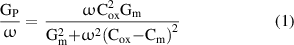
where Cox is the oxide capacitance measured in accumulation, Gm and Cm were measured conductance and capacitance, respectively. ω is the angular frequency of measurement. In the conductance method, Dit can be measured and extracted when the DUT is in the depletion region (or weak inversion). Without any eventual diffusion of Al into bulk silicon and to the Hf-oxide, Dit for all the DUTs should be measured at the same voltage. However, the DUT A and B are measured in the range from 3 V to 4 V. And, the DUT C (which has the lowest Al concentration) is measured in the range from 4.4 V to 5.4 V. This is closely associated with the eventual diffusion of Al into silicon or to the Hf-oxide. It is noteworthy that the voltage range used in the conductance method is very dependent of the impurity density in bulk silicon (i.e. Al+3 cation plays a role of contaminating the silicon).
Table 1. Dielectric constant of each sample.
| Sample | Dielectric constant |
|---|---|
| DUT A | 28 |
| DUT B | 30 |
| DUT C | 45 |
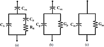
Figure 2. Equivalent circuit diagrams for conductance method: (a) an equivalent circuit model of a MOS capacitor, (b) a simplified equivalent circuit of the MOS capacitor, and (c) a measured circuit of the MOS capacitor.
Download figure:
Standard image High-resolution image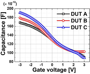
Figure 3. Measured C-V curve of DUT A, B, and C at 1 MHz.
Download figure:
Standard image High-resolution image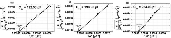
Figure 4. Graphical solution how to obtain the oxide capacitance for (a) DUT A, (b) DUT B and (c) DUT C at 1 MHz frequency.
Download figure:
Standard image High-resolution image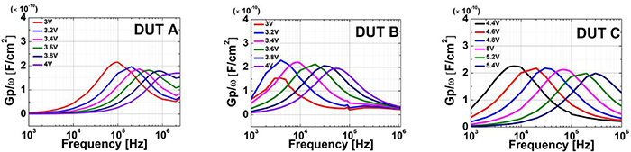
Figure 5. The normalized equivalent parallel conductance vs. frequency as a function of gate bias of (a) DUT A, (b) DUT B and (c) DUT C.
Download figure:
Standard image High-resolution imageFrom the conductance peak shown in figure 5, the interface trap density can be extracted using [24]:
where A is the active area of device. The location of interface traps in the bandgap ( E) can be calculated by Shockley–Read–Hall statistics of capture and emission rates [24]:
where τ = 2π/ω, σ is the capture cross section of the trap,  t is the average thermal velocity of majority carriers, N is the effective density of states of the majority carrier band, k is the Boltzmann constant, and T is temperature. The parameters are summarized in table 2.
Table 2. Parameters used in figure 5.
| Si | |||
|---|---|---|---|
| Property | Unit | n-type | p-type |
| Capture cross section | cm2 | 10–15 | 10–15 |
| Thermal velocity | cm/s | 2.3 × 10⁷ | 1.6 × 10⁷ |
| Density of states | eV−1 cm−3 | 3.2 × 10¹⁹ | 1.8 × 10¹⁹ |
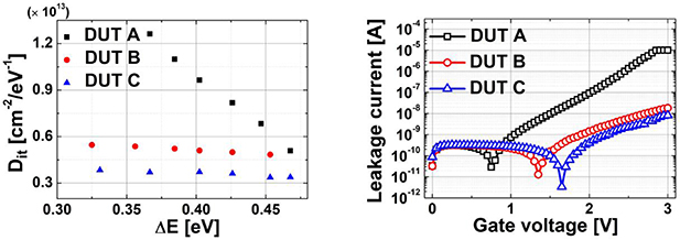
The calculated Dit vs.  E is obtained from the conductance method for all the samples (see figure 6(a)). The Dit of DUT A, B, and C is 1.26 × 1014 cm−2 eV−1, 5.46 × 1013 cm−2 eV−1, and 3.84 × 1013 cm−2 eV−1, respectively. The values of Dit are still too high to be used in advanced CMOS technology, so that more improvement is necessary to have Dit below 1012 cm−2 eV−1. Note that Dit is distributed between the valence band edge and the mid-gap energy level. It is observed that interface trap density (As a function of energy state) decreases near the mid gap. Figure 6(b) exhibits the leakage current of DUT A, B and C as a function of the gate-to-bulk voltage. From the measured results, DUT C has a lowest gate leakage current due to its lower interface trap density (vs. DUT A, B). This result indicates that an appropriate Al content in HfO2 thin film is necessary to satisfy a specification of leakage current.
Figure 6. (a) Interface trap density (Dit) vs. △E. This is derived from the peak value of conductance spectrum. (b) Comparison of measured leakage current-voltage (I–V) curves of DUT A, B, C for leakage current characteristics.
Download figure:
Standard image High-resolution image
4. Conclusion
Using the conductance method, the interface traps between Al-doped HfO2 and Si are investigated. Three DUTs were fabricated with varying Al concentration in HfO2 layer (i.e. 3:1, 5:1, and 10:1 of HfO2:Al2O3 for DUT A, B, and C, respectively). The measured interface trap density of DUT A, B, and C was 1.26 × 1014 cm−2 eV−1, 5.46 × 1013 cm−2 eV−1 and 3.84 × 1013 cm−2 eV−1, respectively. Because of the lowest Dit in DUT C, it is expected to have the lowest leakage current in Al-doped HfO2 film. In reality, it turned out that the DUT C has formed a good interface state between the insulation and semiconductor.
Acknowledgments
This work was supported by the National Research Foundation of Korea (NRF) through a grant funded by the Korean Government (MSIP) (No. 2020R1A2C1009063).