
Abstract
This paper presents development of flexible metal-semiconductor-metal devices using silicon (Si) microwires. Monocrystalline Si in the shape of microwires are used which are developed through standard photolithography and etching. These microwires are assembled on secondary flexible substrates through a dry transfer printing by using a polydimethylsiloxane stamp. The conductive patterns on Si microwires are printed using a colloidal silver nanoparticles based solution and an organic conductor i.e. poly (3,4-ethylene dioxthiophene) doped with poly (styrene sulfonate). A custom developed spray coating technique is used for conductive patterns on Si microwires. A comparative study of the current–voltage (I–V) responses is carried out in flat and bent orientations as well as the response to the light illumination of the wires is explored. Current variations as high as 17.1 μA are recorded going from flat to bend conditions, while the highest Ion/Ioff ratio i.e. 43.8 is achieved with light illuminations. The abrupt changes in the current response due to light-on/off conditions validates these devices for fast flexible photodetector switches. These devices are also evaluated based on transfer procedure i.e. flip-over and stamp-assisted transfer printing for manipulating Si microwires and their subsequent post-processing. These new developments were made to study the most feasible approach for transfer printing of Si microwires and to harvest their capabilities such as photodetection and several other applications in the shape of metal-semiconductor-metal structures.
Export citation and abstract BibTeX RIS

Content from this work may be used under the terms of the Creative Commons Attribution 3.0 licence. Any further distribution of this work must maintain attribution to the author(s) and the title of the work, journal citation and DOI.
1. Introduction
Flexible electronics are believed to complement the conventional electronics by including also the macro-scaled devices, which were left in pursuit of highly miniaturized electronic systems. Research has been reoriented to fill the wide gap available in almost every field of electronic components for instance in displays, lighting, energy, communications, sensors and actuators etc [1–5]. A variety of interesting proof of concept devices and prototypes have been produced by industrial as well as academic research institutes [1, 4, 6–10]. Besides new devices concepts, the flexible electronics field also requires the development of new types of materials and processing technologies that could lead to their cost-effective manufacturing. One of the significant attractions is their manufacturing on a large scale through high-speed roll to roll processes [3, 10, 11]. Solution based printing technologies are the backbone of such high-speed manufacturing. Organic based materials have the advantages of being solution processed and mechanically flexible, which makes them favorable for printing technologies. However, organic based materials suffer from serious challenges such as lower mobility, fast degradation, limited to ambient temperature operations and short lifetime etc [12, 13]. Reliability is a key concern of any electronic device, which is seen as very challenging to be achieved by using only organic materials. Therefore, the need for heterogeneous integration of multi-functional organic and inorganic materials is highly desired to overcome these challenges.
Amongst the list of inorganic semiconductor materials, silicon (Si) has remained the first choice for wafer based electronics owing to its matured processing as well as well-known excellent mechanical and electrical properties [4, 13]. Si in the shape of thin microwires has attracted significant interest in recent years for its possible integration to flexible substrates through transfer printing [14–18]. Dominating the conventional wafer based electronics for several decades, these thin Si microwires have shown preliminary promising results in different devices authenticating its bright future in the field of flexible electronics as well [7, 14–17, 19–21]. Tunable electrical properties by changing the type and doping concentrations efficiently, these high aspect microwires are foreseen to have a significant contribution towards the development of variety of flexible devices and sensors [14, 17, 22, 23]. To effectively utilize the Si microwires and design a process protocol for successful fabrication of devices, materials with compatible electrical and mechanical properties are highly desirable to maintain the higher electrical performance as well as mechanical flexibility of the devices. The higher surface-to-volume ratio of the Si microwires make it interesting for these diverse applications. After dry transfer printing of the Si microwires, a feasible as well as cost-effective patterning technique for the metal contacts is needed. The low-cost printing technologies especially inkjet printing and spray coating are the most promising approaches for such applications.
Metallic patterning of Si microwires takes the lead right after successful transfer on flexible substrates. Therefore, an investigation of the electrical response of different interfacing materials is of prime interest. Observations of the organic conductors interfacing Si microwires are investigated in this research and compared the resulting values to the metallic counterpart. An asymmetric metal semiconductor metal (MSM) structure is selected for these investigations due to its simple structure and easy manufacture. Asymmetric MSM are recently introduced devices, which have potential applications in various fields such as solar fuel cells, artificial photosynthesis, strain sensors, piezo-phototronics etc [14, 23, 24]. MSM photodetectors are also very stimulating owing to their good electrical bandwidth, fast response, small capacitance, large available active area to be used as flexible optical sensors [8, 25, 26]. For completing the asymmetric MSM structure, only patterned deposition of the conductor materials is required. Therefore, a custom-made spray setup is used to coat two different conductor solutions to evaluate the performance of each conductor with Si microwires. Metallic solution based on silver (Ag) nanoparticles and an organic conductor i.e. PEDOT-PSS are used for these experiments. Investigation is further extended for MSM structures utilizing two differently doped (n and p type) Si microwires in separate devices. Finally, the optical response of MSM structures are also evaluated at different light (visible and ultra violet (UV)) illuminating intensities to explore the possibilities of Si microwires as building block for flexible photodetectors.
2. Materials and experimental procedures
2.1. Metal-semiconductor-meta (MSM) structures
MSM heterojunctions are contacts between two different materials resulting in very interesting electrical and optoelectronic properties [8, 14, 26, 27]. These types of contacts are significant since they are present in all electronic devices in the shape of a discrete component, or an intrinsic part of the device. A potential barrier is formed when metal has contact with a semiconductor, which is responsible for controlling the current conduction and its capacitance behavior [28]. The difference of the work function of the two contacting materials is very critical and this difference could be adjusted either by choosing a suitable metal or by changing the doping concentration of the semiconductor [29, 30]. Their behavior is mainly dependent on the interface characteristics resulting into either schottky or ohmic contacts [29, 30]. Most of the solution processed materials developed recently for flexible electronics show deviations in the experimental barrier heights from the ideal conditions, which are due to either an unavoidable interface layer or the presence of interface states [12, 29–31]. Therefore, a proper selection of materials and the manufacture process is needed, where a controlled deposition of materials and patterning is performed. Si microwires developed through standard photolithography and the commercialized conductive materials provide an opportunity to overcome these limitations. The transfer of thin Si microwires on any secondary substrates and subsequent materials used for metal patterning approve the manufacture of MSM structures on diverse substrates (schematics and band diagrams of used materials shown in figures 1(a) and (b)). These devices have attracted significant interest in the field of flexible electronics [8, 14, 26, 28, 29]. Therefore, this research presents the feasible route to manufacture these devices by manipulating the transfer technique, type of Si microwires, different materials for conductive patterning and eventually evaluating the current response in dark as well as different light illuminations.
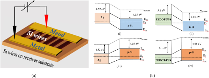
Figure 1. (a). Schematics of metal-semiconductor-metal (MSM) structure. (b) Band diagram of the contacting materials.
Download figure:
Standard image High-resolution image2.2. Si microwires and transfer printing
Differently doped (n- and p-type) of Si microwires are used in the investigation of MSM structures. The detailed description about fabrication of Si microwires and transfer printing them onto secondary flexible substrates are discussed elsewhere [7, 19]. The possibility to manipulate both types of p- and n-doped Si microwires on flexible substrates and using them in realizing electronic structures is investigated. For this purpose, the p-type microwires were developed on the Si on insulator (SOI) wafers (p-type) as received without altering the doping concentration. Whereas doping of the n-type wires is accomplished by implanting phosphorous during the photolithography process. SOI wafers are assisted in maintaining the thickness uniformity of the Si microwires, which is essential for any semiconductor layer in electronic devices. Corresponding width and thickness of Si microwires are 50 μm and 2.5 μm respectively with 10 μm trench gap between each consecutive microwires. The optical profilometer graph and microscopic images shown in figure 2 authenticates the microwires uniformity. As against the solution based printed semiconductors, the thickness and bulk properties of the semiconductor are maintained before and after transfer printing onto secondary substrates. There is negligible effect on the thin Si microwires during the whole process including the oxide layer etching, transfer to carrier stamp and finally printing on the secondary substrate.

Figure 2. Microwires width and thickness uniformity check with optical profilometer of the under-etched Si microwires before transfer. Inset: optical images of etched Si microwires with tethered points. Corresponding width and thickness of microwires are 50 μm and 2.5 μm respectively with 10 μm gap between each consecutive microwires.
Download figure:
Standard image High-resolution imageSi microwires are under-etched and transferred to secondary substrates through a PDMS stamp. In addition to the stamp-assisted transfer (figures 3(a)–(f)) [32], the flipped-over (figures 3(g)–(h)) Si microwires are also characterized for the current–voltage (I–V) and optical response measurements. Flip-over is the type of dry transfer technique in which the Si microwires are directly transferred to a polyimide (PI) substrate with one side adhesive. After etching the buried oxide layer, the adhesive side of the PI (mounted on a carrier support) is brought in conformal contact with the suspended microwires as shown in the figures 3(g)–(h). As against the stamp-assisted transfer printing, flip-over is more simple being a single step process. The main challenge faced by flip-over transfer printing is the exposure of bottom side of the Si for post-processing and device fabrication. As during the transfer printing, the top finished surface comes in direct contact with the adhesive layer, which is sacrificed for the sack of transferring wires to flexible substrate. The restricted device configuration after flip-over transfer limits the use of Si microwires to very few applications. In addition, the incompatibility of the adhesive glue on the PI substrate with some of the chemicals used during the post-processing degrades the adhesion causing detachment of the Si microwires from the flexible substrates. Therefore, to investigate and confirm these claims, flipped-over n- and p-type Si microwires are characterized and compared to the I–V and optical response of the stamp-assisted transfer printed Si microwires.
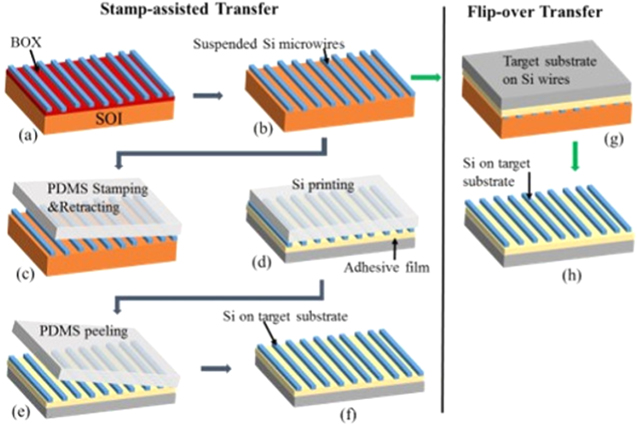
Figure 3. (a)–(f). Steps involved in stamp assisted transfer printing of Si microwires using a PDMS stamp, (g)–(h). Flip-over transfer printing of Si microwires.
Download figure:
Standard image High-resolution image2.3. Silver-based solution for spray coating
Solution-based conductive inks have remained central to the advancement of printed and flexible electronics. These colloidal solutions are easily printed at room temperature having a desired conductor in the shape of nanoparticles dispersed in respective solvents. The lower temperature processing makes these solutions compatible with diverse polymeric substrates. The conformable integration of conductive patterns and strong adhesion to non-conventional polymeric substrates after printing has provided sufficient confidence to work with these materials. Amongst the list of available solution processed conductors with stable properties, silver (Ag) has emerged as the most promising in terms of synthesis, processing, robustness and more stability for a longer time after curing on flexible substrates [33, 34]. Silver has been used in electronic devices since the birth of microelectronics and remains the most prominent material for diverse applications in emerging technologies. Several other metallic materials including both organic and inorganic have also been developed for conductive patterns such as copper, gold, platinum and tin [3, 11, 35]. Allotropes of carbon in the form of CNTs and graphene are considered suitable conductors for flexible electronics recently owing to their intrinsic mechanical flexibility while possessing higher conductivities [31, 35]. However, developing stable solutions with longer shelf life and more resistant to oxidation during pre-and post-printing steps. As against, the promising properties of long storage life, good printability on diverse substrates and reliable conductivities for long time make Ag colloids an attractive option amongst other solution-based conductors [11]. The easy and matured synthesis process for a stable solution with tunable rheological properties have made silver a first choice in conductive solutions.
In this research silver paste (DuPont 5028) was selected for the conductive patterns of MSM structures. The Ag paste is commonly used to develop low voltage circuitry, especially on flexible substrates [11, 33]. The composition is particularly suitable for applications requiring higher conductivities and fast curing. It can be used on fast speed roll-to-roll, semiautomatic and manual printers by offering prolonged residence time on the dispensers. The silver paste is primarily developed for screen-printing technology, which has higher viscosity in the range of 15–30 Pa S as per supplier (DuPont) specifications. Inkjet and spray coating technologies required lower viscosities in the range of 0.001–0.10 Pa S as compared to viscosities desired for screen printing which is in the range of 0.50–5 Pa S [3]. Therefore, to make the solution less viscous, a suitable thinner as recommended by the supplier i.e. DuPont 3610 is added to the paste in appropriate ratios to lower the viscosities compatible with desired inkjet/spray coating processes. A hard mask is used for the patterned deposition through spray coating, which is explained with more details in subsequent sections.
2.4. Patterning PEDOT-PSS by spray coating
The future scope of flexible electronics is believed to have higher mobility and lower manufacturing costs to complement the conventional electronics. The higher speeds come by introducing inorganic semiconductors into the stack of materials having intrinsic flexibility [13]. Processability of inorganic semiconductors such Si microwires and then transferring to secondary flexible substrates comes with relatively higher costs. Therefore, to compensate the unavoidable higher costs of the Si microwires, choosing the cost-effective materials and fabrication techniques for the post-processes are among the possible alternatives to reduce the overall costs. Organic conductors are solution-processable, inherently flexible [36] and integrating these with inorganic semiconductors would lead to devices that are more economical in future. Integration of organic conductors and inorganic semiconductor is seldomly reported in printed flexible electronics filed, therefore in this research we have studied the possible heterogeneous integration of dissimilar materials in the form of thin films. Among the list of available conductive polymers, poly (3,4-ethylene dioxthiophene) (PEDOT) doped with poly (styrene sulfonate) (PSS) is the preferred choice for their distinguished mechanical and electrical properties [24, 36, 37].
PEDOT-PSS is an organic conductor with higher mechanical flexibility and relatively good thermal stability [38]. PEDOT can be chemically polymerized in a poly (styrenesulfonic acid) (PSS) solution to give a PEDOT-PSS water emulsion. It results into a conjugated polymer with positively doped properties, where the PSS are the counter ions used to balance the doping charges [39]. The transparent nature of ultrathin PEDOT-PSS layers has played significant role in developing flexible optoelectronic devices [24, 36, 40]. These devices are mainly targeted for solar cells and energy applications utilizing also organic semiconductors or blend materials. However, utilizing PEDOT-PSS as a transparent conductive [36] contact to Si microwires for the development of MSM structures would be a step further towards more innovative devices. These structures could possibly result in development of exciting applications as flexible photodetectors, mixers, strain cum optical sensors and flexible optical switches. PEDOT-PSS suffers from lower conductivities; however, research is in progress for exploring effective secondary doping to enhance the conductivity of PEDOT-PSS [38, 39]. The secondary dopant is an inert substance, which further increases the conductivity of the primarily doped (with PSS) conjugated polymer [39]. It has been observed that conductivity of PEDOT-PSS can be enhanced by more than one order of magnitude by addition of polyalcohols (alcohols with more than two OH groups on each molecule) [37]. Conductivity of PEDOT-PSS can rapidly be enhanced by treating the film with only methanol which have one OH group [38]. The possibility to enhance the conductivity of PEDOT-PSS compared to other polymeric conductors is a plus point to use it for high-end devices. Solution used for spray coating in these experiments was purchased form Sigma Aldrich (product no. 739332). A high-conductivity grade solution is prepared with a concentration of 1.1% in H2O. Further specifications as per supplier include resistance <100 Ω sq.−1, <80% visible light transmission (40 μm wet), refractive index n20/D 1.334, PH < 2.5, viscosity <100 cP (22 °C) and with a density of 0.999 g ml−1 at 25 °C.
2.5. Printing experiments
The Si microwires were developed by photolithography and released from the SOI donor wafer by under-etching the buried oxide. Details about the wires fabrication strategies and transfer printing are discussed elsewhere [7, 19]. The two transfer strategies as i.e. stamp-assisted and flip-over are schematically presented in figures 3((a)–(f) and (g)–(h) respectively). The Si microwires are transferred to two different flexible substrates i.e. PET and PI substrate with one side adhesive. Selection of these substrates is related to the adaptation of transfer printing approach for Si microwires. PET substrate is optically transparent and is the most feasible substrate for the stamp-assisted transfer. The PET substrate is coated with optically transparent adhesive layer i.e. SU-8 (3000 series, MicroChem), which serves as the receiving medium for the Si microwires. Another advantage of adhesive SU-8 layer is its sensitivity to UV light, which promotes the rapid transfer of Si from the stamp when brought in conformal contact to the receiving medium. The rapid curing of SU-8 when exposed to UV light from the backside of the substrates promotes the Si microwires transfer efficiently to the target PET substrate along curing of the SU-8 layer. This completes the second transfer and the wires are ready for post-processing. In case of PI substrate, the adhesive part does not require any post-treatment and the wires are transferred just in one-step as shown in schematics (figures 3(g)–(h)).
Patterning of the conductive tracts of the MSM structures were carried out as a post-process to transfer printing by using spray coating. Spray coating is a direct writing technique where the solution is injected by a syringe pump, transported through a teflon tubing and carried through the tip of a nozzle [41, 42]. Various types of spray configurations are practiced in microelectronics of which the most common are electrospray and aerospray. In electrospray, configuration of the system remains the similar to aerospray except the nozzle types and actuation procedures. The actuation mechanism of the electrospray is governed by application of a high electric field between the nozzle and a counter electrode. In this setup, an electric field is generated between the two electrodes to ionize the fluid. Positive potential is applied to the capillary nozzle while ground is applied to the conductive plate kept at a certain distance below the nozzle tip [41, 42]. Despite the capability to deposit an ultrathin layer with minimum surface roughness, the complex system parameters and specific requirements of solution conductivities to get primarily a stable cone-jet are more challenging. Additionally, the localized heating due to high electric field is undesirable for organic based materials as it results in nozzle clogging by immediate sintering of the materials in the nozzle. On the other hand, aerospray deposition is a good alternative having almost similar spray coating results but with more simplified operation.
A dual concentric nozzle is used in aerospray deposition, whereas the internal nozzle is used to deliver the fluid while the external is used for air/N2 flow to atomize the fluid into spray. Rheological properties of the solution are adjusted especially the viscosity to ease the spraying of the solution. Figures 4(a) and (b) shows optical images of the concentric nozzle and system setup for the aerospray coating developed in this research. A dual concentric (coaxial nozzle) purchased from NanoNC Korea is connected with the syringe pump (Harvard Apparatus, PhD 2000 Infusion) through a Teflon tubing. Syringe pump is used to control the flow rate. A higher flow rate i.e. 2000 ml min−1 is applied initially to flood the nozzle and then reduced to around 500 ml min−1 during the spraying process. For the silver solution, stage is heated at around 120 °C whereas for PEDOT-PSS the stage temperature is kept around 100 °C. For the patterned deposition, a hard mask is used with two line openings.

Figure 4. Optical images and schematics of (a). Dual concentric nozzle (Coaxial Nozzle, NanoNC, Korea). (b) Schematic of the cross-sectional view of the nozzle. (c) Spray system configuration with nozzle stand, heated substrate and a syringe pump. (d) Shadow mask prepared from brass by milling machine. (d) Ag spray on Si microwires (50 μm wide and 50 μm wide trenches), (e). PEDOT-PSS spray patterning on flexible substrates.
Download figure:
Standard image High-resolution imageA rigid and high temperature resistant material is desired for the hard masks to maintain the firm attachment to the flexible substrate without damaging Si microwires. Initially a 3D printed shadow masks were used [7]. These masks were prepared from stack of polymeric sheets glued to each other automatically by the 3D printer. They are ideal for solutions which does not require substrate heating during the deposition. However, for the metal deposition, this 3D printed shadow masks are challenging, as the stacked layers are unglued during the heating process and deteriorates the final structures. In addition, the firm attachment to the substrate and microwires is a serious issue and the solution undergoes through the elevated parts of the mask resulting into short-circuiting of the conductive contacts. Thin sheet of brass (50 μm thick) is ideal for such applications that is rigid and can withstand higher temperatures at the same time as shown in figure 4(c). To make the fabrication of mask more robust, patterns are developed through a milling machine.
3. Results and discussions
The asymmetric MSM structures (figures 4(d) and (e)) were characterized in planar as well as bent orientations. The I–V measurements were performed in ambient environment by probing both the metals contacts using semiconductor parameter analyzer (4156 C, Agilent). Main purpose of these investigations was to compare the performance of both types of Si microwires independently on separate substrates under different conditions. Further investigation considered in this study are analysis of the two-step stamp-assisted transferred wires and flipped-over transferred wires. Investigations is also carried out on the junction characteristics of Ag and PEDOT-PSS with both types (n- and p-Si) of microwires. For optical characterization, MSM structures were illuminated with visible and UV light with various. A halogen lamp light with varying light intensity that is integrated to the microscope of the probe station is used to shine light from the top on microwires. Whereas an UV light source was used to find the current response of the microwires compared to halogen light. The light intensity is varied for six different values ranging from 102 μW cm−2 to 13.29 mW cm−2. The UV-light source has a fixed value so the lamp is kept at two distant positions to vary the intensity of light falling on the microwires. Intensity of UV-light at position 1 was 7.22 mW cm−2 and 22 mW cm−2 at position 2.
3.1. I–V Measurements of planar MSM structures
Devices were characterized based on the combination of differently doped Si microwires arrays. For the first combination of devices made of p- and n- doped Si wires on separate substrates and by making the metal contacts using Ag. Graphs in figures 5(a) and (b) show I–V measurements of the MSM devices in planar orientations. The highest current values of Ag/n-Si-Ag is observed to be 7.72 μA at a positive bias of 5 V whereas maximum of −12.8 μA at negative bias of −5 V without any light illumination. Alternatively, the MSM structures made of Ag/p-Si/Ag have a highest current value of 0.14 μA for the positive biased voltage of 5.0 V and −0.73 μA for the negative bias of −5 V. The difference in the current response of the Si microwires is obvious owing to the differently doping and doping concentrations as well. Doping concentration of n-Si microwires with P is about 1015 whereas p-type wires are moderalty doped with boron (B) i.e. 1012. Traps formed at the junction and the difference in the junction potentials between Ag with the n and p-type Si microwires might also be adding to the current response variations. The work function differences (figure 1(b)) of both the materials is another factor affecting the variations in the current responses.
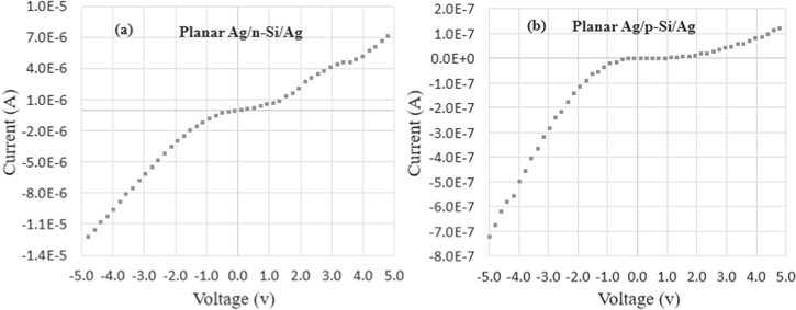
Figure 5. I–V measurement of the MSM structures by using Ag with, (a). n-Si microwires and, (b). p-Si microwires separately in planar mode.
Download figure:
Standard image High-resolution imageSimilarly, the devices were characterized made of PEDOT-PSS as a conducting contact to p- and n-Si on separate substrates. The asymmetric MSM structure having PEDOT-PSS as the immediate conductive contact to the Si microwires, while silver paste is used as the contacting pad for the probe test. PEDOT-PSS is observed to have poor attachability to the flexible substrate and declined even further by doping with ethanol. Therefore, to avoid deterioration of thin PEDOT-PSS layers, devices are characterized by putting probes on the silver spots instead directly contacting the PEDOT. After Spray coating of PEDOT-PSS, the patterned layers are sintered at 120 °C. To enhance the conductivity of PEDOT layers, ethanol was drop casted following the technique explored in [38]. The graphs in figures 6(a) and (b) show I–V curve for the PEDOT/n-Si/PEDOT and PEDOT/p-Si/PEDOT, respectively, in planar mode. The current response is not very rapid for the hybrid junctions made between PEDOT/n-Si/PEDOT. PEDOT is usually used as hole injection material in optoelectronic devices where its conductive behavior and transmittance in the visible range of light make it a good substitute for metals with no transmittance at all. An inversion layer is formed on the surface of n-type Si microwires as a result of large work function difference between the PEDOT (ФPEDOT 4.7–5.4 eV) and n-Si (Фn-Si, ∼3.85 eV). Strong inversion occurs at the interface and the junction behaves more like a p–n junction diode [27, 43]. On the other hand, PEDOT/p-Si/PEDOT shows very promising results due to the lower junction potential and minimal difference in the work functions of PEDOT (ФPEDOT 4.7–5.4 eV) and p-Si (ФPEDOT 4.95 eV). A moderate Schottky junction at lower voltage and ohmic in the medium range is observed for the dark current measurement as shown in figure 6(b). Further, the current start to saturate at very low voltage, making the device ideal for other applications such as low voltage thin film transistor. The higher current response in the saturation regime is in acceptable range for diverse transistor and switching applications in lightweight flexible electronics.
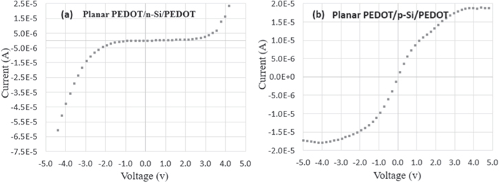
Figure 6. I–V measurement of the MSM structures using PEDOT with, (a). n-Si microwires, (b). p-Si microwires separately in planar mode.
Download figure:
Standard image High-resolution image3.2. I–V Measurements of MSM in bend orientation
The similar MSM structures were characterized in the bend orientation and compared the values with the planar ones for possible changes in the current response of the Si microwires as a result of tensile strain. Two rectangular blocks (as shown in figure 7) were used at fixed positions using bi-adhesive tape and the plastic substrates were fixed between the edges of two blocks. The blocks were kept at 15 mm apart making a circular radius of around 7.5 mm at the center, where maximum strain is to be observed in the microwires. The microwires were characterized in the convex position as shown in figure 7. Significant change in the resistance of the n-Si wires is observed as shown in figure 8(a) compared to the planar counterparts shown in figure 5(a). The maximum dark current response in the planar mode at positive bias of 5.0 V is 7.72 μA, whereas the same devices under bend conditions have a maximum current response of about 0.48 μA, which represents a significant increase in the resistance of Si microwires. On the other hand, the I–V curve for Ag/p-Si/Ag in bend mode experiences very less changes as shown in figure 8(b) compared to the I–V curve of the similar devices in planar mode shown in figure 5(b). The lower doping concentration of p-Si might be one of the reason for these less variations compared to the prominent variations in the heavily doped n-Si microwires. Another reason for the less variations is due to the non-uniform spacing between the metallic contacts. Deviations in the spacing could also lead to the variations in the response of microwires, as the wires with increased spacings would be subjected to more strain compared to closely spaced conductive patterns. The closely spaced metal patterns act as a supporting layer to prevent the Si microwires from undergoing any strain. This needs further investigation and in order to harvest the strain response of the Si microwires, spacing between the metal contacts need to increase.

Figure 7. Current–voltage (I–V) measurements of Si microwires in bent (15 mm diameter) (a). I–V under halogen lamp with varying intensities and (b) under UV-light.
Download figure:
Standard image High-resolution image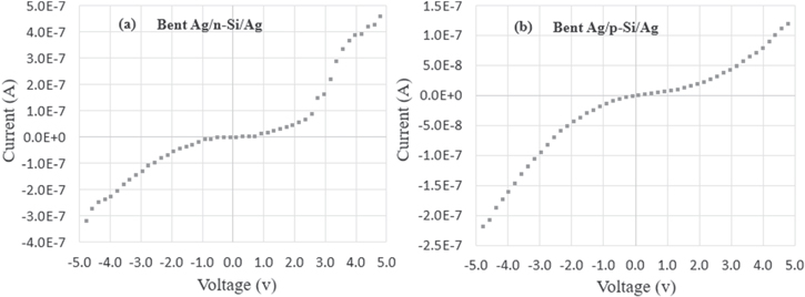
Figure 8. I–V measurement of the MSM structures by using Ag with, (a). n-Si microwires and, (b). p-Si microwires separately in bent orientation.
Download figure:
Standard image High-resolution imageFigures 9(a) and (b) show I–V curves of the PEDOT/n-Si/PEDOT and PEDOT/p-Si/PEDOT respectively in bend mode. In this case, significant variations were observed for both the devices compared to the current values in planar mode. For the PEDOT/n-Si/PEDOT, the dark current reduces from 25.0 μA (figure 6(a)) to 7.9 μA (figure 9(a)) for the positive biased of 5.0 V. The current response for the PEDOT/p-Si/PEDOT have less variations in the bend mode against planar. The dark current reduces from 18.3 μA (figure 6(b)) to 2.33 μA (figure 9(b)) in the bend mode, which is again due to the less doping concentration of the p-Si. All these variations in the current response in planar and bend mode of the MSM structures lead to interesting applications of using Si microwires as strain sensors [22, 23]. The slight changes in the orientation either convex or concave have a strong bearing on the current response of the microwires, which could successfully be utilized as a strain sensor. These type of devices are attractive for applications such as prosthetic limbs and synthetic or electronic skin (e-skin) for robots where various dexterous manipulation tasks are monitored.

Figure 9. I–V measurement of the MSM structures by using PEDOT with (a). n-Si microwires and, (b). p-Si microwires separately in bent orientation.
Download figure:
Standard image High-resolution image3.3. Photodetection and optical switching of the MSM
Photodetectors and especially UV photoswitches have emerged as vital components for a wide range of commercial applications including biological and chemical analysis, flame monitoring, missile detection, secure space communication and astronomical studies [8]. The transfer of Si microwires on flexible substrates presents an attractive role in realizing visible and UV photodetection owing to their high surface-to-volume ratio. The high responsivity and photodetection gain has been traditionally found in the low-dimensional wide bandgap materials such as GaN, ZnO, TiO2 and several metal-oxide bandgap nanostructures [44, 45]. However, the high sensitivity to ambient environment such as temperature and humidity making these devices more prone to signal fluctuations and poor selectivity. Another main issue with some of these materials is the low recovery time mainly due to their photo-gain predominantly governed by their surface states. These devices are less durable and have a short life in such variable and harsh environments [8, 45]. Additionally, the major challenge with the wide bandgap materials is their reliable integration onto flexible substrates. To overcome these issues, Si μ-wires have been investigated as alternative to detect broad spectrum in visible and UV range.
The MSM structures were characterized for the optical response with different illuminations as shown in figure 7. Halogen lamp with a broad spectrum of visible light was used with variable light intensity summarized in table 1. The wires were illuminated with 6 different values of the light intensity and corresponding change in the current response was measured. The minimum light intensity was 102 μW cm−2 and maximum as 13.29 mW cm−2. In the second type of illumination, a UV light source is used at two different intensities. The light intensities were monitored by using an optical meter. The halogen light is integrated with the microscope of the probe station and the light source was right on top of Si microwires. Whereas in case of UV light, the lamp was kept on the side facing directly at an angle (∼45°) to the Si microwires.
Table 1. Intensities of the light sources.
| Halogen lamp | Intensity (mW cm−2) |
|---|---|
| Photo 1 | 0.12 |
| Photo 2 | 0.407 |
| Photo 3 | 1.417 |
| Photo 4 | 2.91 |
| Photo 5 | 6.85 |
| Photo 6 | 13.29 |
| UV lamp | |
| Photo UV 1 | 7.22 |
| Photo UV 2 | 22.0 |
The MSM devices based on Ag contact with both n- and p-Si were characterized under illumination conditions in planar mode with similar method described in previous section (3.2). Graphs in figure 10(a) shows comparison of current responses of n-Si microwires with light illumination of UV and halogen lamp. The dark current in the graphs of figure 10(a) corresponds to the values without light and are compared to the current gains with light illuminations. The current gains are observed with two different light sources i.e. a halogen light source namely photo 5 with intensity of 6.85 mW cm−2 and two values of UV lamp i.e. 7.22 and 22 mW cm−2. The Ag/n-Si/Ag structures are observed to have more current gains under exposure to the halogen lamp even with lower intensity (6.85 mW cm−2) than the one with maximum UV-light (i.e. 22 mW cm−2). The maximum change observed with the light illumination is 27.4 μA, three times higher than the peak value of dark current at the positive bias of 5.0 V. On the negative bias side, increase in the current values by more than two order of magnitude i.e. 30.4 μA is observed as compared to 12.8 μA of the peak dark current at −5.0 V. The maximum Ion/Ioff ratio 3.22 is obtained with the halogen lamp illumination. On the contrary, not much change is observed with UV illumination. Possible reasons for the inconsistent and lower current response to UV light in figures 10(a) and (b), are the lower penetration of UV light through the Ag layer. This restricts the enhancement of charge injection at the Ag–Si interface. Besides this the minor imperfections and trap charges at the interface might also have significant effect on the lower current values. However, these experiments need further investigation of the interface and traps causing this behavior.
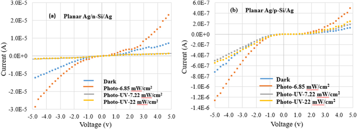
Figure 10. I–V measurement of stamp-assisted MSM structures by using Ag with, (a). n-Si microwires, (b). p-Si microwires separately in planar mode under light illumination of halogen and UV.
Download figure:
Standard image High-resolution imageThe I–V curves in figure 10(b) show the corresponding current values of Ag/p-Si/Ag devices, which are observed to be responsive to both the illuminations. An increase in current gains are observed compared to the dark current values by obtaining Ion/Ioff ratios of 3.85 and 1.92 for the halogen and UV lights respectively. The response is significant again for the halogen light especially on the negative bias where more than one order of magnitude increase in the peak dark current value is observed. However, the UV response is negligible and have adverse effect on current in the negative bias.
Devices made of PEDOT/Si/PEDOT have very promising results in response to light illumination owing to the junction modification between PEDOT and Si microwires. The transmission window in the visible range of PEDOT allows the light to directly interact at the interface and hence increase the number of charge carrier. This has been observed from the experimental values of current gain during the I–V measurements. Figure 11(a) shows current response at dark and gains in current at different illuminating conditions. Again, the junction between p-type PEDOT and n-Si make an inversion layer at the Si surface by depleting all the majority charges (discussed in section 3.1). The moderate schottky-ohmic behavior is dominant (figure 11(a)) behaving more like a pn-junction diode. The current response is lower at lower biasing values and increases abruptly after certain threshold. The current does not saturate and goes on increasing by increasing the biasing voltage. The switching window is very small by increasing intensity of the halogen lamp. The strong optical switching behavior is shown by the PEDOT/p-Si/PEDOT structures, where the photo current is increased by few order of magnitudes as shown in figure 11(b). As against the previous devices (Ag/Si/Ag), here the UV response of the current is higher in both the positive and negative biasing voltages. The junction is moderately modified from schottky like junction towards more ohmic with the gradual increase of the light illumination as shown in figure 11(b). The photocurrent gains (46.5 μA) increases by an amount of 28.2 μA compared to the dark current (18.3 μA). Similar trend of current enhancement is observed on the negative bias as well. The peak current values increase approximately by four orders of magnitude by illuminating the Si microwires with UV-light at higher light intensity i.e. 22 mW cm−2. The maximum Ion/Ioff value calculated for both the n- and p-Si devices with EPDOT as the interfacing electrode are 1.6 and 4.51 respectively.
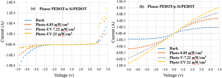
Figure 11. I–V measurement of stamp-assisted MSM structures by using PEDOT with, (a). n-Si microwires, (b). p-Si microwires separately in planar mode under light illumination of halogen and UV.
Download figure:
Standard image High-resolution imageReal-time optical switching of the PEDOT/Si/PEDOT was also investigated, where a lower biasing voltage i.e. 0.5 V was applied to the MSM structures and the light is switched on and off during the biasing conditions. The switching behavior is evident from the figures 12(a) and (b), where halogen and UV lights are illuminated respectively on a PEDOT/n-Si/PEDOT structure. Both the graphs show an increasing value of the current with increased biasing, however by turning off the light an immediate loss in the current value is observed as shown in figures 12(a) and (b). A significant variation in the current values is detected during the light-on and light-off conditions. For instance, at biasing voltage of 0.5 V, the peak current value for light-on is 11.5 μA, whereas the current value drops to 1.5 nA with the light-off. The trend of change in the current values is same at each value of the biasing voltage.

Figure 12. I–V response and switching behavior of the MSM structures using PEDOT with n-Si microwires separately, (a). Light illumination of halogen, (b). UV light.
Download figure:
Standard image High-resolution imageThe significant difference in the current gains just by turning-on and off the illuminating light is a very promising result for development of a flexible optical switch as well as photodetection. The fast response time i.e. sharp increase and decline in the current gains without any delay (figures 12(a) and (b) by turning on/off the light sources present unique characteristics. An enhanced optical current response is observed for the UV light compared to the halogen lamp. An increased current value of 40.2 μA is detected at biasing voltage of 0.5 V with the light-on and drops to 2.3 nA with UV light-off. The increase in current gain with UV light-on i.e. 28.7 μA compared to halogen light-on at similar biasing voltages (0.5 V) confirms the superior performance of the optical switch for UV light with a wider operating and switching window. Figures 13(a) and (b) show graphs of switching behavior of a PEDOT/p-Si/PEDOT structure. The switching current window is small in case of p-Si due to the less charge carrier concentrations compared to the heavily doped n-Si (doping concentration is 1015). The variations in the photocurrent and dark current is very small for both the types of illuminations. In order to make the switching window wider, a higher doping concentration is desired. The overcoming of charge trap sites at the PEDOT/p-Si/PEDOT devices and increasing the doping concentration of the charge carriers might help in lowering down the current to the baseline value.

Figure 13. I–V response and switching behavior of the MSM structures using PEDOT with p-Si microwires separately, (a). Light illumination of halogen, (b). UV light.
Download figure:
Standard image High-resolution image3.4. I–V of flipped-over Si microwires
Flip-over transfer printing is a one-step process for an easy and simple transfer of Si microstructures from the donor wafer onto secondary flexible substrates. All the devices discussed in previous sections were transferred to flexible substrates using a PDMS-stamp, which involves a two-step transfer process. Wires are picked-up by weak Van der Waals forces from the donor wafer through a PDMS stamp. A very planar stamp is desired for such transfer process and a high active surface area of contact between the wires and stamp is needed. Serious risk involved in this process is some wires cannot be detached from the tethered points and remain attached to the wafer. However, this could be avoided by over-etching by completely removing the buried oxide. The over-etching approach is more effective for wires with wider dimension such as 30–40 μm widths or more. Wires with lower widths i.e. less than 20 μm are difficult to control as the wires are detached from the anchored positions after completing the etching of buried oxide. Additionally, cleaning steps such as with deionized water to remove the etchants (BHF), wires can detach during this and the subsequent handling steps. Therefore, under-etching is desired for the type of structures having higher resolutions both in width and in thickness. In such scenario, a flip-over transfer, where the flexible substrates have one side adhesive such as scotch tapes are more helpful. Here the interface of stronger adhesive layers and the under-etched microstructures is stronger and the wires could easily be transferred onto the target substrates.
To validate these remarks, experiments were performed using a polyimide substrate with adhesive on one side. The PI was fixed on a glass slide, the adhesive side facing upwards. After etching the Si microwires (30 μm wide) and the cleaning steps, the glass slide is contacted to the donor wafer and removed back directly without any delay. Transfer yield in this approach is 100% as all the microwires were transferred onto the PI tape. Despite the higher transfer yield, this procedure also has serious challenges of the pre-and post-processing for the substrate as well as for the microwires. No patterning or metallization is supported by the PI adhesive layer before transferring. With pre-metallization, there is serious risk of deteriorating the adhesive layer used for Si microwires detachment from donor wafers. Therefore, only top metallization or post processing after the transfer step is possible in this approach. Additionally, the adhesive part of the substrate is not compatible with most of the cleaning solvents (i.e. acetone or ethanol required for removal of the PSS layer after deposition of the PEDOTT-PSS for conductive contacts) making the process more challenging. Another issue is for the metal contacts, as backside of the Si device layer is available for the post-processing, therefore getting an ohmic contacts at the junctions are at risk. This is less critical for the structures requiring single type of doped semiconductors (like for MSM) structures; however, for complex devices such as transistors and CMOS devices, different doping sections are desired within a single structure.
Experimental investigation has been carried out to compare the current response and the junction behavior of the flipped-over Si microwires to that of stamp-assisted transfer printed microwires. The MSM structures from the flipped-over microwires have been developed with the similar procedure as followed for the stamp-assisted microwires. The I–V measurements for the Ag/n-Si/Ag and Ag/p-Si/Ag are given in figures 14(a) and (b) respectively. Comparing the current response of Ag/n-Si/Ag and Ag/p-Si/Ag in figures 14(a) and (b) with current values of corresponding stamp-assisted devices in graphs in figures 10(a) and (b) respectively, the schottky behavior is dominant with the flipped-over wires. The dark current and current gains at the higher biasing voltages are in close ranges for the n-Si wires. A lower Ion/Ioff ratio is determined by the n-Si devices i.e. 1.58, whereas the Ion/Ioff for the p-Si devices is higher i.e. 6.53 compared to the corresponding stamp-assisted devices. The Ion/Ioff ratios are in acceptable ranges however, the net current values are very less than the corresponding stamp-assisted devices. Thickness of the n-Si is lower (500 nm) than the p-Si (2.5 μm) and therefore the doping concentration is uniform on both the side. The variations in the junction contacts might be due to the increased traps and residual oxide, affecting the ohmic behavior even under illuminations. Comparing the results of figures 15(a) and (b) with that of the corresponding devices in figures 11(a) and (b) respectively, the major deviations in the current response as well as the junction behavior are evident. The Ion/Ioff ratios observed for both n-Si and p-Si devices are 0.98 and 43.8 respectively. Similar to the Ag/Si/Ag devices, the PEDOT/Si/PEDOT devices also present very low current values despite the highest on/off ratios for the PEDOT/p-Si/PEDOT devices. The current drops by 6.22 μA in the PEDOT/n-Si/PEDOT structure along with a strong schottky junction. A lower current response i.e. 0.12 μA is experienced with the PEDOT/p-Si/PEDOT (figure 15(b)) with the flipped-over microwires as compared to the 18.3 μA with the stamp assisted transferred microwires. The junction does not change for higher illuminations despite the lower difference in the work functions of PEDOT and p-Si and transmission window of the PEDOT to the visible light. Table 2 summarizes all the peak currents of all the corresponding MSM devices in planar mode and the maximum Ion/Ioff ratios among the two illuminating conditions. It is evident from the current responses that flip-over currents are lower compared to the dark as well photocurrent of the stamp-assisted transferred Si microwires. Additionally, the provision to pre-process the substrate for the back contacts and availability of the finished top Si device surface for post-processing make the stamp-assisted transfer printed microwires more attractive. The large window of optical switching, higher value of photocurrent and junction modification from schottky to ohmic junction under illumination make PEDOT/p-Si/PEDOT more interesting for practical applications as in flexible electronic systems.
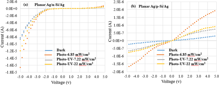
Figure 14. I–V of flipped-over structures (a). Ag/n-Si/Ag, (b). Ag/p-Si/Ag in planar mode, characterized also for light illumination of halogen and UV.
Download figure:
Standard image High-resolution image
Figure 15. I–V of flipped-over structures (a). PEDOT/n-Si/PEDOT, (b). PEDOT/p-Si/PEDOT in planar mode. Characterized also for light illumination of halogen and UV.
Download figure:
Standard image High-resolution image
Table 2. Summary of corresponding peak current of the planar Si μ-wires.
| Transfer type | Type of devices | Peak dark current (μA) at 5.0 V. | Peak photo 5 current (μA) at 5.0 V. | Peak photo UV 2 current (μA) at 5.0 V. | Maximum Ion/Ioff |
|---|---|---|---|---|---|
| Stamp-assisted transfer printed | Ag/n-Si/Ag | 7.22 | 23.2 | 1.32 | 3.22 |
| Ag/p-Si/Ag | 0.13 | 0.5 | 0.25 | 3.85 | |
| PEDOT/n-Si/PEDOT | 7.6 | 12.2 | 7.18 | 1.60 | |
| PEDOT/p-Si/PEDOT | 18.3 | 46.5 | 82.5 | 4.51 | |
| Flip-over transfer printed | Ag/n-Si/Ag | 0.6 | 0.953 | 0.6 | 1.58 |
| Ag/p-Si/Ag | 0.3 | 1.96 | 0.907 | 6.53 | |
| PEDOT/n-Si/PEDOT | 10 | 9.89 | 2.58 | 0.98 | |
| PEDOT/p-Si/PEDOT | 0.1 | 2.46 | 4.38 | 43.8 |
4. Conclusion
This research was carried out for a comparative study of various configurations of asymmetric MSM structures. The two differently doped p- and n-Si microwires were developed by standard photolithography and etching techniques. Stamp assisted and flip-over transfer printing were used to relocate Si microwires to secondary flexible substrates. In stamp assisted approach, more than 90% transfer yield was obtained by using a planar PDMS stamp is to pick and place Si microwires deterministically at desired locations on secondary substrates. On the other hand, 100% transfer yield achieved with flip-over technique by stamping the target substrate to pick the microwires. For conductive patterns, Ag nanoparticles based colloidal solution and an organic conductor i.e. PEDOT-PSS were spray coated by using shadow masks. The MSM structures were characterized both in planar and bent orientations to investigate the I–V response of the microwires. Significant decrease in current values i.e. 7.24 μA of planar Ag/n-Si/Ag is observed while undergoing a convex bend. Similar results of current decrease i.e. 17.1 μA while bending is observed for PEDOT/n-Si/PEDOT devices. The MSM structures were also characterized for the optical illumination of two different light sources, i.e. halogen and UV lamps. PEDOT/p-Si/PEDOT showed maximum responses in dark as well as current gains during illumination. The highest Ion/Ioff ratio i.e. 43.8 is presented by flipped-over PEDOT/p-Si/PEDOT devices for the current gains of 4.38 μA. The rapid changes in the current gains for turning on and off the light illumination present attractive results for fast optical switches.
The evaluation of the transfer printing procedures was also central to the investigation within this research. Despite the simple processing and acceptable current responses, flip-over Si microwires have several drawbacks hindering their usage for useful applications. The non-availability of the top-finished surface of Si device layer is one of the major obstacles resulting in the lower current values as shown in table 2. Additionally, it is more challenging to pattern conductive contacts on the adhesive layer at the pre- and post-transfer stage. Processing to pattern would deteriorate the adhesive layer, ultimately affecting the microwires adhesion to the PI substrate. On the other hand, stamp assisted transfer printed Si microwires on PET substrate are possible to be patterned before spin coating the adhesive layer. Therefore, microwires transferred through stamp-assisted transfer have more attractions to be used for diverse applications. For instance, a back-gated MISFET structure is essential for using these microwires for sensor, where the top functionalized surface is available for direct interaction with the transducer materials. These back-gated structures are also interesting for optical related application such as UV and visible light detection, artificial photosynthesis and fuel cells etc.
Acknowledgments
This work was supported by the European Commission under grant agreement PITN-GA-2012-317488-CONTEST and Engineering and Physical Sciences Council (EPSRC) Fellowship for Growth—Printable Tactile Skin (EP/M002527/1).