
Abstract
We investigate the strain evolution and relaxation process as function of increasing lattice mismatch between the GaAs core and surrounding InxGa1−xAs shell in core–shell nanowire heterostructures grown on Si(111) substrates. The dimensions of the core and shell are kept constant whereas the indium concentration inside the shell is varied. Measuring the  and
and  in-plane Bragg reflections normal to the nanowire side edges and side facets, we observe a transition from elastic to plastic strain release for a shell indium content x > 0.5. Above the onset of plastic strain relaxation, indium rich mounds and an indium poor coherent shell grow simultaneously around the GaAs core. Mound formation was observed for indium contents x = 0.5 and 0.6 by scanning electron microscopy. Considering both the measured radial reflections and the axial 111 Bragg reflection, the 3D strain variation was extracted separately for the core and the InxGa1−xAs shell.
Export citation and abstract BibTeX RIS

Original content from this work may be used under the terms of the Creative Commons Attribution 4.0 licence. Any further distribution of this work must maintain attribution to the author(s) and the title of the work, journal citation and DOI.
Introduction
Compared to planar heteroepitaxy, the formation of axial or radial heterostructures in the form of nanowires has opened up new horizons for the design of heterostructures in a more efficient and less costly way [1–5]. One of the most beneficial qualities of core–shell nanowires is surface passivation of the core by the surrounding shell which can be utilized to enhance the efficiency of photo-emission because it reduces non-radiative surface recombination [6, 7] and thereby enhances the opto-electronic properties of the device [8–10].
Strain relaxation in core–shell nanowires has been thoroughly investigated in recent years, revealing higher sustainability of elastic strain compared to planar heterostructures [11, 12]. Above a critical lattice mismatch between the core and shell materials, the misfit strain can relax via the formation of misfit dislocations [13, 14], quantum dots [15, 16] and stress-driven surface roughening [17, 18]. The aforementioned strain relaxation mechanisms within the nanowire core–shell system strongly depend on the diameter of the core, thickness of the shell and the lattice mismatch between the core and shell. For instance, Treu et al have reported that a 10 nm thick InAs0.91P0.09 shell grows coherently around an InAs core. However, an InP shell of the same thickness shows the formation of dislocations [19]. Furthermore, it was revealed that the photoluminescence emission of this core–shell nanowire system exacerbates for higher P contents within the shell. This indeed indicates that the investigation of the strain relaxation mechanisms and critical composition of core–shell nanowires are of paramount importance for the fabrication of high performance devices with nanowire heterostructures.
Moreover, a novel strain relaxation process was recently revealed by Lewis et al 2017 [20] for GaAs nanowire cores surrounded by Inx Ga1−x As shells. Based on lab x-ray diffraction of the axial 111 Bragg reflection and transmission electron microscopy measurements, it was demonstrated that above a critical lattice mismatch, plastically relaxed mounds form along the nanowire sidewall facets. The relaxed mounds and a coherent shell grow simultaneously from the beginning of Inx Ga1−x As deposition such as, driven by strain relief, incoherent mound growth is increasingly favored for higher lattice mismatches. Furthermore, it was unveiled that the mounds are indium rich compared to an indium poor shell. However, Lewis et al did not measure the radial lattice parameters preventing 3D strain analysis.
In this work, we complement the above-described measurements by recording reciprocal space maps (RSMs) of the  and
and  Bragg reflections which are orthogonal to the nanowire growth axis, and normal to the side edges and side-facets, respectively from GaAs\Inx
Ga1−x
As core–shell nanowires with 20% ≤ x ≤ 60% In. From these diffraction maps, on the one hand, we confirm the appearance of plastic strain relaxation for the highest In content of 60%, resulting in the simultaneous growth of indium rich mounds and an indium poor Inx
Ga1−x
As shell, in agreement with [20]. However, the formation of mounds is observed for indium concentrations of 50% and above by scanning electron microscopy (SEM). We extend on these findings by calculating the 3D strain of the GaAs core and Inx
Ga1−x
As shell at the edges and side-facets, revealing a strain variation of the core which reaches its maximum for nanowires with 50% of indium in the Inx
Ga1−x
As shell. Notably, for an indium concentration of 20%, the crystal lattice of the Inx
Ga1−x
As shell at the side-facets and edges undergoes 3D compression whereas the GaAs core expands along and perpendicular to the growth direction regardless of the lattice mismatch.
Bragg reflections which are orthogonal to the nanowire growth axis, and normal to the side edges and side-facets, respectively from GaAs\Inx
Ga1−x
As core–shell nanowires with 20% ≤ x ≤ 60% In. From these diffraction maps, on the one hand, we confirm the appearance of plastic strain relaxation for the highest In content of 60%, resulting in the simultaneous growth of indium rich mounds and an indium poor Inx
Ga1−x
As shell, in agreement with [20]. However, the formation of mounds is observed for indium concentrations of 50% and above by scanning electron microscopy (SEM). We extend on these findings by calculating the 3D strain of the GaAs core and Inx
Ga1−x
As shell at the edges and side-facets, revealing a strain variation of the core which reaches its maximum for nanowires with 50% of indium in the Inx
Ga1−x
As shell. Notably, for an indium concentration of 20%, the crystal lattice of the Inx
Ga1−x
As shell at the side-facets and edges undergoes 3D compression whereas the GaAs core expands along and perpendicular to the growth direction regardless of the lattice mismatch.
Experiment and results
The samples investigated in this work are GaAs/Inx Ga1−x As core–shell nanowires grown by molecular beam epitaxy using the Ga-assisted vapor−liquid−solid growth on n-type Si(111) substrates covered by native oxide. The core diameter and shell thickness are kept constant at 140 nm and 18 nm respectively whereas the nominal indium concentration inside the shell is varied from 20% to 60% with steps of 10% for the five investigated samples (samples 1–5). A detailed description of the nanowire growth procedure can be found elsewhere [20]. SEM micrographs of nanowires from samples 1–5 are displayed in figure 1. The nanowires from samples 1–3 display a smooth surface whereas nanowires from samples 4–5 show exterior presence of mounds. However, the number density and relative size of the mounds is smaller for sample 4 (discussed later).

Figure 1. Panels (a)−(e) show SEM images of nanowires from samples 1−5, respectively. The scale bar in (a) is 1 μm and applies to all SEM images.
Download figure:
Standard image High-resolution imageThe x-ray diffraction measurements were carried out on as-grown nanowire ensembles at beamline BL9 [21] of the DELTA synchrotron (Dortmund, Germany) with 1 mm2 beam and photon energy of 13 keV. To access the radial strain normal to the side facets and edges of the core and shell, rocking scans were performed in the vicinities of the  and
and  in-plane Bragg reflections collecting the scattered intensity distribution using a two dimensional 100 k Pilatus detector placed 1 meter away from the sample. The experiment was executed in grazing incidence geometry where the angle of the incident beam with respect to the substrate surface was set to zero and the diffracted intensities of the
  and
and  Bragg reflections were measured in the plane perpendicular to the surface normal at Bragg angles at around 27.6° and 48.80°, respectively. The 2D intensity frames collected at each rocking angle were integrated to compose 2D RSMs of the respective Bragg reflections. More information about the diffraction setup, and equations used to translate from real space angular coordinates into reciprocal space vectors can be found in [22]. From the width of a Si
  substrate reflection measured at the same beamline under identical conditions (same beam energy, detector, sample to detector distance and beam size) an angular resolution of about 0.05° can be inferred.
RSMs of the  and
and  reflections are displayed in panels (a)–(e) and (f)–(j) of figure 2, respectively, ranging from samples 1 to 5 (from left to right). Reciprocal space vectors
  and
and  are defined along the scattering direction of the measured planes in reciprocal space. In other words,
  and
and  are sensitive to the variation in the spacing of the respective lattice planes. Reciprocal space vectors
  and
and  are defined along [
 ] and [
 ] respectively, and are sensitive to the nanowire tilt along the corresponding directions.
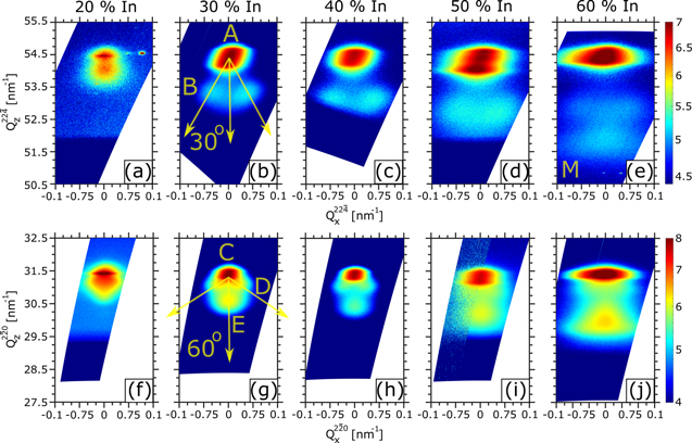
Figure 2. Panels (a)–(e) and (f)–(j) show RSMs of the  and
and  Bragg reflections for samples 1–5 respectively. All maps are plotted using the same color scale. The nominal indium concentration of each sample is mentioned on top of the each panel. Peaks A-E and M are explained in text.
Download figure:
Standard image High-resolution imageThe scattering peaks, named A-E, in the RSMs of figures 2(b) and (g) can be explained by the strain impact on the lattice planes of different sections of the core–shell nanowire system [22–24]. For better clarity, a schematic correlation between the respective RSMs recorded for sample 2, and sketches of the core–shell nanowire cross-section overlapped by the  and
and  lattice planes are illustrated in figures 3(a) and (b). Peak A in the
  RSMs originates from the
  lattice planes of the GaAs core and the Inx
Ga1−x
As side facets that are aligned vertically onto the side walls of the core in figure 3(a). The two sub-peaks B, indicated by red arrows at lower
lattice planes of the GaAs core and the Inx
Ga1−x
As side facets that are aligned vertically onto the side walls of the core in figure 3(a). The two sub-peaks B, indicated by red arrows at lower  values, make an angle of 30° with [
 ] and therefore originate from the
  lattice planes of the neighboring Inx
Ga1−x
As side facets. The slight asymmetry in the intensity of the split peaks B for samples 2–4 (figures 2(b)–(d)), clearly seen in figure 3(a) for sample 2, where the peak on the right is more intense than the left one, can be attributed to the asymmetry of the (In,Ga)As shell i.e. the opposing side facets of the shell contributing to the right diffraction peak are thicker than the opposing side facets contributing to the left diffraction peak. This slight asymmetry can, in turn, result in a small nanowire bending which is responsible for the slanting of peak A for samples 2–4. The inhomogeneity of the shell may originate from the geometry of the evaporation sources with respect to the substrate in the growth chamber. Interestingly for sample 5, an additional sub-peak, labelled by M, is visible at low
lattice planes of the neighboring Inx
Ga1−x
As side facets. The slight asymmetry in the intensity of the split peaks B for samples 2–4 (figures 2(b)–(d)), clearly seen in figure 3(a) for sample 2, where the peak on the right is more intense than the left one, can be attributed to the asymmetry of the (In,Ga)As shell i.e. the opposing side facets of the shell contributing to the right diffraction peak are thicker than the opposing side facets contributing to the left diffraction peak. This slight asymmetry can, in turn, result in a small nanowire bending which is responsible for the slanting of peak A for samples 2–4. The inhomogeneity of the shell may originate from the geometry of the evaporation sources with respect to the substrate in the growth chamber. Interestingly for sample 5, an additional sub-peak, labelled by M, is visible at low  values (see figure 2(e)), presumably originating from the Inx
Ga1−x
As mounds (see figure 1(e)). The same is expected for sample 4, as will be extended on later, but it is not visible due to the smaller scanning range (figure 2(d)). We attribute peak C in the
values (see figure 2(e)), presumably originating from the Inx
Ga1−x
As mounds (see figure 1(e)). The same is expected for sample 4, as will be extended on later, but it is not visible due to the smaller scanning range (figure 2(d)). We attribute peak C in the  RSMs to Bragg diffraction from the
  lattice planes of the GaAs core. Sub-peaks D, making an angle of about 60° with [
 ], are explained by diffraction from the
  lattice planes of neighboring Inx
Ga1−x
As side facets. Peak E, indicated by a red circle in figure 3(b), belongs to the
lattice planes of neighboring Inx
Ga1−x
As side facets. Peak E, indicated by a red circle in figure 3(b), belongs to the  lattice planes of the measured couple of Inx
Ga1−x
As opposite side facets that are aligned horizontally with the GaAs core.
lattice planes of the measured couple of Inx
Ga1−x
As opposite side facets that are aligned horizontally with the GaAs core.

Figure 3. (a) and (b) Top rows show sketches of the core–shell nanowire cross-section oriented along  and
and  illustrating the lattice planes of the respective reflections. RSMs of the
  and
and  Bragg reflections of sample 2 are displayed in the bottom row. Peaks A-E are explained in text.
Download figure:
Standard image High-resolution imageQualitatively, the central peaks appearing at  = 54.5 nm−1 and
  = 31.5 nm−1 broaden along
  and
and  for increasing nominal indium concentration in the Inx
Ga1−x
As shell. The broadening along Qz
reflects the higher strain variation that the core undergoes whereas the broadening along Q
x
resembles a higher angular tilt of the nanowires with respect to the substrate normal as the core–shell lattice mismatch increases. The broadest peak is observed for nanowires with 50% of nominal indium content. This is the transition point from elastic deformation to plastic strain relaxation via the formation of Inx
Ga1−x
As aggregates found by [20].
for increasing nominal indium concentration in the Inx
Ga1−x
As shell. The broadening along Qz
reflects the higher strain variation that the core undergoes whereas the broadening along Q
x
resembles a higher angular tilt of the nanowires with respect to the substrate normal as the core–shell lattice mismatch increases. The broadest peak is observed for nanowires with 50% of nominal indium content. This is the transition point from elastic deformation to plastic strain relaxation via the formation of Inx
Ga1−x
As aggregates found by [20].
To estimate the strain variation in the core, the radial  and
and  lattice constants and indium content of the Inx
Ga1−x
As shell, we integrate the
lattice constants and indium content of the Inx
Ga1−x
As shell, we integrate the  and
and  Bragg reflections along Qx
and fit the resulting Qz
line profiles, displayed in figure 4 with multi-Gaussians.
Bragg reflections along Qx
and fit the resulting Qz
line profiles, displayed in figure 4 with multi-Gaussians.
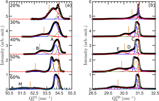
Figure 4. (a) and (b) show waterfall intensity integrations of the  and
and  RSMs in figure 2. The red dashed lines at
  = 54.5 nm−1 and
  = 31.5 nm−1 indicate the positions of unstrained GaAs. The cut vertical orange lines represent the positions of unstrained
  and
and  Inx
Ga1−x
As for the nominal indium concentration of the sample. The colored Gaussian fits are explained in text.
Inx
Ga1−x
As for the nominal indium concentration of the sample. The colored Gaussian fits are explained in text.
Download figure:
Standard image High-resolution imageThe red dashed lines at  = 54.5 nm−1 and
  = 31.5 nm−1 in figure 4 indicate the positions of the respective unstrained lattice planes for GaAs. The cut vertical orange lines represent the positions of unstrained
  and
and  Inx
Ga1−x
As lattice planes for the nominal indium concentration of the sample. The red curves represent peaks B and E in
Inx
Ga1−x
As lattice planes for the nominal indium concentration of the sample. The red curves represent peaks B and E in  and
and  respectively. The most intense peaks in
  and
and  are peaks A and C. Their broadening originates from the strain variation acting on the respective lattice planes of the GaAs core for peak C, and from the
  lattice planes of the core and the Inx
Ga1−x
As facets which are aligned vertically on the sides of the core (see figure 3(a)) for peak A. Representing the lower and upper edges of this variation by the green and blue Gaussians, the strain variation can be calculated from the difference between these two peaks. The values of the strain variation calculated accordingly for the GaAs core for samples 1–5 are listed in table 1. The pink Gaussian peak along [
lattice planes of the core and the Inx
Ga1−x
As facets which are aligned vertically on the sides of the core (see figure 3(a)) for peak A. Representing the lower and upper edges of this variation by the green and blue Gaussians, the strain variation can be calculated from the difference between these two peaks. The values of the strain variation calculated accordingly for the GaAs core for samples 1–5 are listed in table 1. The pink Gaussian peak along [ ] represents sub-peaks D. Conventionally, the Bragg peak of the substrate, supposed to be unstrained, is used as a reference to calculate the absolute strain in the nanowires. However, due to the absence of the Si peak in the in-plane diffraction pattern, we set the right edge of the core peak (colored in green in figure 4) to the position of unstrained GaAs for both
  and
and  All other peaks have been shifted subsequently. This is an approximation because the GaAs core is affected by a small tensile strain induced by the surrounding shell which results in a tiny shift towards lower Qz
values. However, this effect is neglected. The Inx
Ga1−x
As shell of the nanowires in sample 1 is compressed as the red peak is centered at a higher
All other peaks have been shifted subsequently. This is an approximation because the GaAs core is affected by a small tensile strain induced by the surrounding shell which results in a tiny shift towards lower Qz
values. However, this effect is neglected. The Inx
Ga1−x
As shell of the nanowires in sample 1 is compressed as the red peak is centered at a higher  value compared to the unstrained position assuming the nominal In content, which is indicated by a vertical cut line. For samples 2 (30% In) and 3 (40% In), the red Gaussian is almost centered at the
  values of unstrained In0.3Ga0.7As and In0.4Ga0.6As which leads to two possible explanations. The first is that the Inx
Ga1−x
As shell is fully relaxed whereas the second is that the Inx
Ga1−x
As shell is strained, but the tetragonal distortion is at an angle, so the compression and expansion mostly cancel out resulting in an average peak that is found at the unstrained
values of unstrained In0.3Ga0.7As and In0.4Ga0.6As which leads to two possible explanations. The first is that the Inx
Ga1−x
As shell is fully relaxed whereas the second is that the Inx
Ga1−x
As shell is strained, but the tetragonal distortion is at an angle, so the compression and expansion mostly cancel out resulting in an average peak that is found at the unstrained  However, the
  Bragg reflection of the Inx
Ga1−x
As shell being visible at lower
Bragg reflection of the Inx
Ga1−x
As shell being visible at lower  with respect to the unstrained value (peak E) indicates that the Inx
Ga1−x
As lattice, in agreement with [20], is indeed strained and therefore negates the first explanation. For sample 5 (60% of indium), two peaks colored in red and cyan are visible along
with respect to the unstrained value (peak E) indicates that the Inx
Ga1−x
As lattice, in agreement with [20], is indeed strained and therefore negates the first explanation. For sample 5 (60% of indium), two peaks colored in red and cyan are visible along  and
and  The cyan peaks are at lower
  and
and  values compared to the unstrained position whereas the red Gaussians are at higher ones. This indicates that the Inx
Ga1−x
As shell is indeed formed of two volumes with different indium concentrations higher and lower than 60%. As the nanowires of samples 4 and 5 show the formation of mounds at the nanowire surface (see figures 1(d) and (e)), Inx
Ga1−x
As of sample 4 would be expected to be represented by two Bragg peaks, similar to sample 5. However, the relatively lower number density and smaller size of the Inx
Ga1−x
As mounds of sample 4 (figure 1(d)) compared to those of sample 5 (figure 1(e)) indicate the early stage of mound formation and thereby the smaller impact the mounds have on the Inx
Ga1−x
As shell. This will be expanded on in the discussion part.
values compared to the unstrained position whereas the red Gaussians are at higher ones. This indicates that the Inx
Ga1−x
As shell is indeed formed of two volumes with different indium concentrations higher and lower than 60%. As the nanowires of samples 4 and 5 show the formation of mounds at the nanowire surface (see figures 1(d) and (e)), Inx
Ga1−x
As of sample 4 would be expected to be represented by two Bragg peaks, similar to sample 5. However, the relatively lower number density and smaller size of the Inx
Ga1−x
As mounds of sample 4 (figure 1(d)) compared to those of sample 5 (figure 1(e)) indicate the early stage of mound formation and thereby the smaller impact the mounds have on the Inx
Ga1−x
As shell. This will be expanded on in the discussion part.
Table 1. Strain values along [ ] and [
 ] for the GaAs core (calculated with respect to unstrained GaAs from the blue curves using equation (1)) and the Inx
Ga1−x
As shell and mounds (calculated with respect to unstrained Inx
G1−x
aAs from the red and cyan curves using equation (1), and plotted in figure 5. The strain values along [111] are taken from [20].
] for the GaAs core (calculated with respect to unstrained GaAs from the blue curves using equation (1)) and the Inx
Ga1−x
As shell and mounds (calculated with respect to unstrained Inx
G1−x
aAs from the red and cyan curves using equation (1), and plotted in figure 5. The strain values along [111] are taken from [20].
 (%) (%) |
 (%) (%) |
 (%) (%) | |||
|---|---|---|---|---|---|
| In | Blue–Green | Red | Blue–Green | Red | |
| 20% | 0.10 ± 0.10 | −0.62 ± 0.92 | 0.05 ± 0.12 | −0.45 ± 2.03 | 0.45 |
| 30% | 0.55 ± 0.63 | −0.03 ± 1.13 | 0.42 ± 0.25 | 0.55 ± 0.97 | 0.70 |
| 40% | 0.44 ± 0.38 | −0.30 ± 0.72 | 0.48 ± 0.28 | 0.44 ± 1.02 | 0.96 |
| 50% | 1.02 ± 0.29 | −0.01 ± 0.81 | 0.96 ± 0.21 | 0.57 ± 1.78 | 0.74 |
| 60% | 0.44 ± 0.34 | 0.96 ± 1.22 (mounds) | 0.37 ± 0.23 | 0.93 ± 1.07 (mounds) | 0.46 |
| −1.00 ± 0.83 (shell) | −0.63 ± 3.71 (shell) | ||||
The percentage lattice difference of the strained (In,Ga)As shell, mounds and GaAs core with respect to unstrained GaAs along [ ] (
] ( ) and [
 ] (
] ( ) can be calculated from the peak positions extracted from the Gaussian curves (red and cyan for the (In,Ga)As shell and mounds, respectively; blue for the GaAs core) using the equation below,
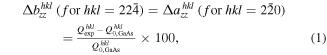
where  is the position of unstrained GaAs along the respective [hkl] direction in Qz
and
is the position of unstrained GaAs along the respective [hkl] direction in Qz
and  is the experimental peak positions of the Gaussian curves. The results are plotted in figures 5(a) and (b).
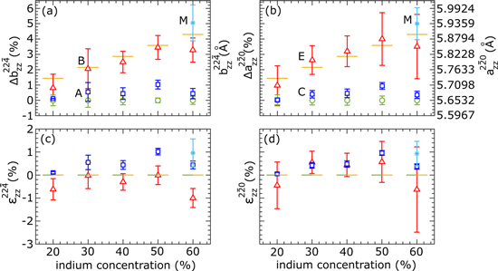
Figure 5. (a) and (b) display the percentage lattice difference of the strained shell, mounds and GaAs core with respect to unstrained GaAs along [ ] (
] ( ) and [
 ] (
] ( ). The spacing between the red dots and the orange cut lines represent the strain acting on the Inx
Ga1−x
As shell as explained in the text below figure 4. The blue and green data points represent the right and left edges of the diffraction peak which originates from the core (figure 4). The cyan data points represent the Inx
Ga1−x
As mounds for 60% of indium. The strain variation of the core and the strain acting on the Inx
Ga1−x
As shell and mounds along [
). The spacing between the red dots and the orange cut lines represent the strain acting on the Inx
Ga1−x
As shell as explained in the text below figure 4. The blue and green data points represent the right and left edges of the diffraction peak which originates from the core (figure 4). The cyan data points represent the Inx
Ga1−x
As mounds for 60% of indium. The strain variation of the core and the strain acting on the Inx
Ga1−x
As shell and mounds along [ ] and [
 ] are plotted in panels (c) and (d).
Download figure:
Standard image High-resolution imageThe strain variation of the GaAs core is calculated from the blue curves using equation (1) since the green curves are already shifted to the position of unstrained GaAs ( =
=  = 0), and the strain acting on the Inx
Ga1−x
As shell and mounds was calculated from the red and cyan curves replacing
= 0), and the strain acting on the Inx
Ga1−x
As shell and mounds was calculated from the red and cyan curves replacing  by
by  which is the position of unstrained Inx
Ga1−x
As along the respective [hkl] direction in Qz
. The numerical strain values are listed in table 1 and plotted in figures 5(c) and (d).
which is the position of unstrained Inx
Ga1−x
As along the respective [hkl] direction in Qz
. The numerical strain values are listed in table 1 and plotted in figures 5(c) and (d).
The colors of the data points in figure 5 are correlated with those of the Gaussian fits in figure 4. As the green curves and cut orange lines in figure 4 were attributed to unstrained GaAs and Inx
Ga1−x
As, the respective inplane strain values being zero were represented by horizontally stitched green and orange lines at  =
=  = 0 (figures 5(c) and (d)). On the one hand, looking at the separation between the blue data points and green lines, the strain variation in the core reaches a maximum of 1.02 ± 0.29% and 0.96 ± 0.21% along
  and
and  for the sample with 50% of indium content before decreasing down to 0.44 ± 0.34% and 0.37 ± 0.23% for the sample with 60% of indium. The values of the strain variation for samples 1–5 are listed in table 1. On the other hand, the strain acting on Inx
Ga1−x
As is represented by the separation between the red data points and the cut orange lines (figures 4 and 5). The red data points of samples 2–4 being centered at positive
for the sample with 50% of indium content before decreasing down to 0.44 ± 0.34% and 0.37 ± 0.23% for the sample with 60% of indium. The values of the strain variation for samples 1–5 are listed in table 1. On the other hand, the strain acting on Inx
Ga1−x
As is represented by the separation between the red data points and the cut orange lines (figures 4 and 5). The red data points of samples 2–4 being centered at positive  values (figure 5(d)) compared to
  reveal that the
  lattice planes of the Inx
Ga1−x
As shell undergo higher expansion compared to the
lattice planes of the Inx
Ga1−x
As shell undergo higher expansion compared to the  lattice planes resulting from the compression along [111]. A similar higher lattice expansion along [
 ] has been observed by Balaghi et al 2019 [25] for the GaAs cores when surrounded by thicker Inx
Ga1−x
As shells. Interestingly, for sample 1, the Inx
Ga1−x
As shell is compressed in all directions. For sample 5, the cyan and red data points at higher and lower values compared to
] has been observed by Balaghi et al 2019 [25] for the GaAs cores when surrounded by thicker Inx
Ga1−x
As shells. Interestingly, for sample 1, the Inx
Ga1−x
As shell is compressed in all directions. For sample 5, the cyan and red data points at higher and lower values compared to  =
=  = 0 (see figures 4 and 5) are both associated with Inx
Ga1−x
As. The first originates from an Inx
Ga1−x
As volume with an indium concentration higher than 60% whereas the second shows a lower indium content. The TEM data for this sample from Lewis et al indicated that the mounds are indium rich whereas the Inx
Ga1−x
As shell, coherent to the core, is indium poor. The error bars were calculated taking into consideration the FWHM of the Gaussians as an input for equation (1).
= 0 (see figures 4 and 5) are both associated with Inx
Ga1−x
As. The first originates from an Inx
Ga1−x
As volume with an indium concentration higher than 60% whereas the second shows a lower indium content. The TEM data for this sample from Lewis et al indicated that the mounds are indium rich whereas the Inx
Ga1−x
As shell, coherent to the core, is indium poor. The error bars were calculated taking into consideration the FWHM of the Gaussians as an input for equation (1).
To get a better understanding of the 3D strain behavior in the core and shell, we performed FEM simulations using a single nanowire model composed of a 140 nm thick GaAs core (blue colored volume in figure 6(a)) and 18 nm Inx
Ga1−x
As shell with indium concentration of 30% (colored in red). More details about the numerical input, meshing procedure (figure 6(b)) and calculation scheme can be found in the FEM section of [24]. Iso-surface slices of the axial strain are demonstrated in figure 6(c) where apart from the upper section of the nanowire model, the core and shell share the same lattice parameter. Line profiles of the strain components  and
and  (see figure 3 for orientation) extracted through one pair of opposite side facets and edges are displayed in the panels (d) and (e) of figure 6, respectively. In confirmation to our assumption, the Inx
Ga1−x
As shell shows lattice expansion larger than the expected nominal lattice mismatch, as a result of the compression along the [111] direction. Interestingly, the inner section of the GaAs core shows slight expansion along [111], [
(see figure 3 for orientation) extracted through one pair of opposite side facets and edges are displayed in the panels (d) and (e) of figure 6, respectively. In confirmation to our assumption, the Inx
Ga1−x
As shell shows lattice expansion larger than the expected nominal lattice mismatch, as a result of the compression along the [111] direction. Interestingly, the inner section of the GaAs core shows slight expansion along [111], [ ] and [
 ], faced by compression as one approaches the core–shell interface. For instance, for the nanowire model with 30% nominal indium concentration, the inner volume of the GaAs core undergoes a lattice expansion of 0.15% along [
 ] and a maximum lattice compression of −0.20% at the core–shell interface, forming a strain variation of 0.35%. This is in agreement with the strain variation deduced experimentally from the difference between the green and blue Gaussian peaks of 0.41%. This experimental value might be overestimated because of normalization of the GaAs peak (see above).

Figure 6. (a)–(c) show the core–shell configuration of the nanowire model, the mesh used and the slices of the axial strain along the nanowire axis, respectively. Panels (d) and (e) are line profiles of the strain components  and
and  extracted through the side facets and edges for samples 1–3, respectively.
Download figure:
Standard image High-resolution image
Discussion
The investigation of the strain behavior in nanowire heterostructures is essential for tuning the opto-electronic performance of the device. For instance, the strain induced by growing an Inx Ga1−x As shell onto one side of a mismatched GaAs core has been utilized to control the bending radius of the nanowire [26] which would enable the realization of a complex spatially varying strain field opening up new possibilities for elastic strain and band structure engineering where the latter can be exploited to control the motion of charge carriers within the nanowire [26–28] and therefore tune its optical properties [29]. Moreover, GaAs nanowire cores exhibit reduction of their bandgap by up to 40% when overgrown with lattice-mismatched thick Inx Ga1−x As shells [25].
Nevertheless, for high lattice mismatches (indium content 50% and above), Inx
Ga1−x
As deposition around a thick GaAs core results in the simultaneous growth of an indium poor coherent shell and indium rich Inx
Ga1−x
As mounds [20] (figures 1(d) and (e)). In the present work, this finding is confirmed by the presence of two Inx
Ga1−x
As diffraction peaks along [ ] and [
 ] for sample 5 (red peak for the coherent shell and cyan peak for the mounds in figures 4 and 5). The lattice spacing of the mounds calculates to 5.9537
  corresponding to a mismatch of
  5.3% which is above the theoretical lattice mismatch considering 60% of indium by 1%. This reflects that the mounds are indeed indium rich compared to the Inx
Ga1−x
As shell. The average indium concentration extracted from the cyan diffraction peaks in
5.3% which is above the theoretical lattice mismatch considering 60% of indium by 1%. This reflects that the mounds are indeed indium rich compared to the Inx
Ga1−x
As shell. The average indium concentration extracted from the cyan diffraction peaks in  and
and  using Vegard's law is around 75%, which is reported to reach up to 80% in [20]. The indium enrichment of the mounds coincides with an indium depletion of the neighboring shell regions. The red Bragg peaks representing the coherent Inx
Ga1−x
As shell translates into a mean indium concentration of 45%. However, the homogeneity of the indium distribution within the mounds depends on how indium diffuses from the shell into the mounds. In contrast to sample 5, sample 4 showed only one diffraction peak attributed to the shell and centered at the position corresponding to 50% of indium. This could be due to the short scan range in reciprocal space. However, an additional peak would be expected to be relatively less intense compared to that of sample 5. This could be attributed to the early stage of mound formation resembled by the relatively low number density and small size of the mounds (figure 1(d)) compared to those of sample 5 (figure 1(e)). Indeed, Lewis et al measured the intensity of the relaxed Inx
Ga1−x
As signal from the 111 Bragg reflection, demonstrating a constant value for 20%–40% of indium (attributed to parasitic growth on the substrate) and then an increase in the integrated intensity from 50%. The intensity between 50% and 60% doubles, reflecting the increasing mound volume with increasing In content.
using Vegard's law is around 75%, which is reported to reach up to 80% in [20]. The indium enrichment of the mounds coincides with an indium depletion of the neighboring shell regions. The red Bragg peaks representing the coherent Inx
Ga1−x
As shell translates into a mean indium concentration of 45%. However, the homogeneity of the indium distribution within the mounds depends on how indium diffuses from the shell into the mounds. In contrast to sample 5, sample 4 showed only one diffraction peak attributed to the shell and centered at the position corresponding to 50% of indium. This could be due to the short scan range in reciprocal space. However, an additional peak would be expected to be relatively less intense compared to that of sample 5. This could be attributed to the early stage of mound formation resembled by the relatively low number density and small size of the mounds (figure 1(d)) compared to those of sample 5 (figure 1(e)). Indeed, Lewis et al measured the intensity of the relaxed Inx
Ga1−x
As signal from the 111 Bragg reflection, demonstrating a constant value for 20%–40% of indium (attributed to parasitic growth on the substrate) and then an increase in the integrated intensity from 50%. The intensity between 50% and 60% doubles, reflecting the increasing mound volume with increasing In content.
The GaAs core undergoes a strain inhomogeneity, induced by the surrounding Inx
Ga1−x
As shell, reflected by the broadening of its Bragg reflection along the scattering directions,  and
and  As the indium content within the Inx
Ga1−x
As shell increases from 20% to 50% (increasing lattice mismatch with constant core and shell dimensions), the strain variation acting on the core increases from (0.10 ± 0.10%) to (1.02 ± 0.29%) along [
As the indium content within the Inx
Ga1−x
As shell increases from 20% to 50% (increasing lattice mismatch with constant core and shell dimensions), the strain variation acting on the core increases from (0.10 ± 0.10%) to (1.02 ± 0.29%) along [ ] and from (0.05 ± 0.12%) to (0.96 ± 0.21%) along [
 ]. Interestingly, as the nominal indium content increases to 60% (Sample 5), the GaAs core relaxes as the strain variation drops down to (0.44 ± 0.34%) along [
 ] and to (0.37 ± 0.23%) along [
 ]. Absolute strain reduction has been observed axially for the GaAs core in [20], and can be explained by the favored growth of the mounds rather than a coherent shell for an increasing core–shell lattice mismatch. The thinner the shell is, the less is the amount of strain induced on the core.
The Inx
Ga1−x
As shell at the side-facet acts as a thin layer deposited on top of a GaAs substrate, which compresses along [111] and [ ] (
] ( ) to match the in-plane lattice spacing of the GaAs core (
 ). This biaxial compression translates into expansion of Inx
Ga1−x
As along [
). This biaxial compression translates into expansion of Inx
Ga1−x
As along [ ] (
] ( ). This, indeed, has been experimentally validated and illustrated in figure 5 (red data points). However, for the nominal indium concentration of 20% (sample 2), the Inx
Ga1−x
As shell seems to exhibit hydrostatic or tri-axial lattice compression, which is not understood. The complete opposite is expected for the GaAs core, which is supposed to undergo only slight expansion, due to its much larger volume, which increases when approaching the hetero-interface. Moreover, supported by the FEM simulations in figure 6, the GaAs core is expected to expand in all directions, being pulled apart by the surrounding lattice mismatched shell. Indeed, the GaAs core is simultaneously expanded axially and radially near the hetero-interface at the side-facets (blue data points in figure 5). Similar behavior has been reported before for thin GaAs cores surrounded by a relatively thick Inx
Ga1−x
As shell [25].
). This, indeed, has been experimentally validated and illustrated in figure 5 (red data points). However, for the nominal indium concentration of 20% (sample 2), the Inx
Ga1−x
As shell seems to exhibit hydrostatic or tri-axial lattice compression, which is not understood. The complete opposite is expected for the GaAs core, which is supposed to undergo only slight expansion, due to its much larger volume, which increases when approaching the hetero-interface. Moreover, supported by the FEM simulations in figure 6, the GaAs core is expected to expand in all directions, being pulled apart by the surrounding lattice mismatched shell. Indeed, the GaAs core is simultaneously expanded axially and radially near the hetero-interface at the side-facets (blue data points in figure 5). Similar behavior has been reported before for thin GaAs cores surrounded by a relatively thick Inx
Ga1−x
As shell [25].
Hetero-epitaxy of strained layers gives access to strain engineering. However, radiative recombination takes place at defect free strained layers only. Plastic strain relaxation associated with the formation of dislocations and other defects creates sources for non-radiative recombination of charge carriers [30] and reduce the luminescence intensity [31]. Considering Stranski-Krastanov growth mode known for lateral hetero-structures, there is a critical thickness beyond which misfit dislocations are created acting as non-radiative centers within the complete layer. In this study we demonstrate that in the case of GaAs/(In,Ga)As radial nanowire hetero-structures there exists also a critical indium concentration which changes the epitaxial growth. However, it is shown that a part of the shell remains coherently strained without dislocations where the strain is released through the formation of In rich mounds at the edges of the shell side-facets [20]. In consequence it means that the strained part still can provide radiative recombination as functional element of a respective optical device.
Conclusions
In summary, sharing the same lattice parameter axially, the GaAs core and the Inx
Ga1−x
As shell have different radial lattice spacings. This makes measuring in-plane Bragg reflections by XRD, namely  and
and  which are normal to the nanowire side-facets and edges, the perfect technique to perform a detailed investigation of the 3D strain behavior and variation in the core and the shell separately. Accordingly, we observed an increase in the average strain variation acting on the GaAs core when increasing the indium content from 10% to 50%, and strain relaxation for 50% and 60%. In addition, for indium concentrations of 50% and 60%, simultaneous growth of relaxed indium rich mounds and an indium poor coherent shell takes place. These were represented by two diffraction peaks along [
 ] and [
 ] for the sample with 60% of indium. However, one diffraction peak centered at the position corresponding to 50% of indium was evident for nanowires with nominal indium content of 50% in the shell, presumably due to the small volume of the mounds near the onset of mound formation and thereby the negligible impact on the shell. Furthermore, the lattice planes of the Inx
Ga1−x
As shell showed relatively higher expansion along [
] for the sample with 60% of indium. However, one diffraction peak centered at the position corresponding to 50% of indium was evident for nanowires with nominal indium content of 50% in the shell, presumably due to the small volume of the mounds near the onset of mound formation and thereby the negligible impact on the shell. Furthermore, the lattice planes of the Inx
Ga1−x
As shell showed relatively higher expansion along [ ] compared to [
 ]. Therefore, this technique is ideal for the investigation of the strain evolution and relaxation mechanism in nanostructures which can be correlated with further optical measurements.
Acknowledgments
The authors would like to thank A-K Bluhm for the acquisition of SEM images and M Höricke as well as C Stemmler for maintenance of the molecular beam epitaxy system used for growth. We thank the DELTA machine group for providing synchrotron radiation at beamline BL9 and acknowledge Michael Paulus for support and discussions.
Data availability statement
The data that support the findings of this study are available upon reasonable request from the authors.
Funding
This work was supported by the Deutsche Forschungsgemeinschaft (grant no. Pi217/38). R.B.L. is grateful for additional funding from the Alexander von Humboldt Foundation.