

Abstract
Two-dimensional (2D) semiconducting transition metal dichalcogenides (TMDs) are promising platforms for developing next-generation electronic and optoelectronic devices due to their unique properties. To achieve this, the growth of large single-crystal TMDs is a critical issue. Unraveling the factors affecting the nucleation and domain orientation should hold fundamental significance. Herein, we design the chemical vapor deposition growth of monolayer MoS2 triangles on Au(111) and Au(100) facets, for exploring the substrate facet effects on the domain orientations. According to multi-scale characterizations, we find that, the obtained triangular MoS2 domains present two preferential orientations on the six-fold symmetric Au(111) facet, whereas four predominant orientations on the four-fold symmetric Au(100) facet. Using on-site scanning tunneling microscopy, we further reveal the preferred alignments of monolayer MoS2 triangles along the close-packed directions of both Au(111) and Au(100) facets. Moreover, bunched substrate steps are also found to form along the close-packed directions of the crystal facets, which guides the preferential nucleation of monolayer MoS2 along the step edges. This work should hereby deepen the understanding of the substrate facet/step effect on the nucleation and orientation of monolayer MoS2 domains, thus providing fundamental insights into the controllable syntheses of large single-crystal TMD monolayers.
Export citation and abstract BibTeX RIS
1. Introduction
Two-dimensional (2D) transition metal dichalcogenides (TMDs) have triggered enormous research interests due to their exotic electronic, optical, mechanical, and catalytic properties, etc [1–6]. As very stable 2D semiconductor in the TMDs family, monolayer molybdenum disulfide (MoS2) has promising applications in field effect transistors, photodetectors, integrated circuits and sensors, etc [7–12]. To achieve these, large-area uniform MoS2 monolayers have been successfully synthesized on various substrates by chemical vapor deposition (CVD) routes [13–18]. However, polycrystalline MoS2 films were usually obtained, featured with many grain boundaries caused by the coalescence of randomly oriented domains [19–21]. The high density of grain boundaries were reported to seriously degrade the electrical transport and deteriorate the device performance [22]. In this regard, precisely controlling the orientations of monolayer MoS2 is highly desired to achieve large single crystals on specific substrates through the merging of mono-oriented domains [23–27].
According to the published references, the orientations of monolayer MoS2 strongly depended on the lattice structures and surface symmetries of the substrates [28–34]. Indeed, the lattice matched substrates (such as c-plane sapphire and mica) were selected for the quasi epitaxial growth of monolayer MoS2, resulting in two main orientations (0°/60° rotated), with the formation of only mirror twin boundaries [31–34]. In this way, the density of grain boundaries was largely decreased. Besides, some substrates with distinct lattice symmetries were also employed for the growth of 2D TMDs [35–37]. For example, two-fold symmetric a-plane sapphire was applied to achieve unusual rectangular monolayer MoS2 domains with nearly uniform orientation [37]. The anisotropic substrate structure was proposed to induce the rapid growth of MoS2 along [1–100] direction of a-plane sapphire.
Moreover, the substrate step was also explored to play a critical role in the orientation of 2D materials [25–27, 38–40]. Recently, the unidirectional alignment of monolayer h-BN domains was realized on the vicinal Cu(110) substrate by the coupling of step edges with h-BN zigzag edges [25]. Quite recently, the epitaxial growth of centimeter-scale single-crystal MoS2 monolayer was also achieved on vicinal Au(111), and the step edges of Au(111) were proposed to guide the unidirectional nucleation and growth behavior [27]. However, the correlation and the internal mechanism between the step-edge-induced and the surface-symmetry-guided growth of MoS2 are still not fully addressed with exact experimental data.
The polycrystalline Au substrate has been widely used for the large-area uniform, large-domain, and fast growth of monolayer TMDs [41–43]. The different facets of Au foils were reported to imply tremendous effects on the domain size and coverage of monolayer MoS2 [43]. Large-domain monolayer MoS2 triangles preferentially grow on Au(100) and Au(110) facets rather than on Au(111) facet at higher growth temperature. However, the modulation effect of Au facets on the orientation of MoS2, and further how MoS2 is aligned with different symmetric Au substrates remain unclear. On-site scanning tunneling microscopy (STM) is a powerful technique for characterizing the atomic-scale structures (especially the lattice direction, superstructure and grain boundary structure), as well as the detailed morphology (e.g. surface steps), making it a suitable tool for addressing the above mentioned issues.
Herein, we demonstrate the orientation-controlled growth of monolayer MoS2 triangles on different symmetric Au(111) and Au(100) facets through an ambient-pressure CVD (APCVD) method. The relative orientations of individual monolayer MoS2 domains on different Au facets are determined definitely by statistical results. Moreover, on-site atomic resolution STM technique is introduced to identify the lattice alignment of MoS2 with the underlying Au facets. The correlation among the lattice orientation of MoS2, step direction and the symmetry of the Au facet is thereby clearly unveiled. Furthermore, the possible mechanism for the nucleation and oriented growth of monolayer MoS2 is also discussed in detail.
2. Methods
2.1. Growth of monolayer MoS2 domains on the Au(111) and Au(100) substrates
The growth of monolayer MoS2 triangular domains on Au(111) and Au(100) facets was performed in an APCVD system which was equipped with a 1 inch diameter quartz tube. The growth conditions are the totally same for the two type samples. Sulfur powder (Alfa Aesar, purity 99.5%) was placed outside the hot zone, which was mildly sublimated at ∼102 °C with heating belts. The downstream Au(111) and Au(100) substrates were placed faced downward to the MoO3 powder (Alfa Aesar, purity 99.9%). In a typical growth process, Ar gas with a rate of 10 sccm was used as the carrier gas. The Au substrates were heated to ∼720 °C within 30 min and maintained about 3 min for growth.
2.2. STM characterizations
An Omicron ultrahigh vacuum (UHV) variable-temperature-STM system was utilized under a base pressure better than 10–10 mbar in room temperature. Low temperature Unisoku STM system was also used for the detailed structural characterizations under a base pressure better than 10–10 mbar. The atomic-scale morphologies of MoS2/Au(111) and MoS2/Au(100) were obtained directly by transferring the samples into the UHV chamber, annealed or unannealed in prior to the STM characterizations.
3. Results and discussion
To explore the substrate symmetry effect on the orientation of monolayer MoS2 flakes, two typical Au facets including six-fold symmetric Au(111) and four-fold symmetric Au(100), are selected as the growth substrates. As shown schematically in figures 1(a) and (b), Au(111) and Au(100) substrates demonstrate distinct arrangements of Au atoms, as well as different step directions on the surfaces, which should have significant effect on the orientation of monolayer MoS2.
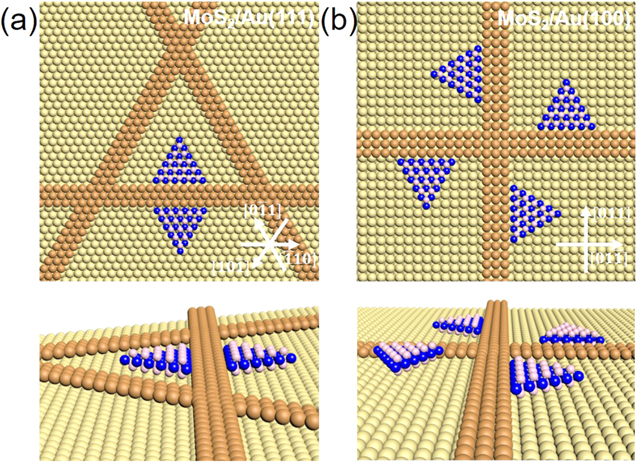
Figure 1. Preferential orientations of monolayer MoS2 triangular domains on Au(111) and (100) facets. (a), (b) Schematics of monolayer MoS2 triangles on six-fold symmetric Au(111) and four-fold symmetric Au(100) facets, respectively. The white arrows show the three equivalent close-packed directions of Au(111) facet in (a), and the two equivalent close-packed directions of Au(100) facet in (b). Brown and yellow atoms denote the step and underlying Au surface, respectively. Blue and pink atoms represent the molybdenum and sulfur atoms, respectively.
Download figure:
Standard image High-resolution imageIn our experiment, Au(111) and Au(100) substrates were firstly prepared by the different annealing methods of Au foils, as also reported previously [27, 44]. Specifically, the single-crystal Au(111) film was achieved by melting and resolidifying the commercial Au foil on a tungsten template at ∼1050 °C for 10 min in an Ar/H2 mixed atmosphere. The Au(100) facet was obtained by annealing the commercial Au foil under a standard process at ∼300 °C for 12 h in an UHV chamber. Electron backscatter diffraction (EBSD) maps in figures 2(a) and (b) confirm the evolution of Au(111) and Au(100) facets, respectively. And then, monolayer MoS2 domains were synthesized directly on Au(111) and Au(100) facets in the APCVD system with MoO3 and sulfur powders as precursors (∼720 °C, ∼3 min) [27, 45].

Figure 2. Facet-dependent orientations of monolayer MoS2 domains on Au(111) and (100) facets. (a), (b) EBSD maps of Au(111) and Au(100) facets, respectively. (c), (d) Representative SEM images of monolayer MoS2 triangles grown on Au(111) and (100) facets, respectively. There are mainly two-orientated MoS2 domains appearing on Au(111) facet whereas four-orientated MoS2 domains on Au(100) facet. The typical orientations of MoS2 on Au(111) and Au(100) are marked by the colored triangles. (e), (f) Statistical histograms of the relative angles of the MoS2 domains on Au(111) and (100) facets, respectively.
Download figure:
Standard image High-resolution imageRaman spectroscopy was firstly performed on the as-grown samples to confirm the formation of monolayer MoS2 (figure S1, available online at stacks.iop.org/NANO/32/095601/mmedia). Two typical peaks corresponding to  and A1g modes of MoS2 occurred at ∼385.0 cm–1 and ∼403.0 cm–1, respectively. The peak position difference of ∼18 cm–1 strongly indicates the monolayer nature of MoS2 [43]. Moreover, the peak positions are nearly identical on the two typical Au facets. The morphology and orientation of the monolayer MoS2 flakes on Au(111) and (100) facets were also analyzed by scanning electron microscopy (SEM). As shown in figures 2(c) and (d), the equilateral triangular MoS2 domains with relatively uniform size and distribution are distinguishable on the Au(111) and (100) substrates. Notably, the triangular-shaped monolayer MoS2 domains appeared on various substrates (e.g. Au foils) were identified as single-crystal domains [27, 28, 34, 46, 47]. This result facilitates the identification and analysis of the MoS2 domain orientations on different symmetric Au facets.
Statistical calculations on the orientations of the monolayer MoS2 domains were subsequently performed. Two preferential orientations of MoS2 on the Au(111) facet can be identified with the relative rotation angles of 0° and 60°, respectively. The ratio of the two type rotated domains is nearly 1:1, as revealed by the quantitative orientation distribution histogram (figure 2(e)). Herein, the specific orientation angle of a monolayer MoS2 domain is defined as the rotation angle (θ) with respect to the selected triangular domain (illustrated in the upper right inset of figure 2(e)). Such 0°/60° rotated MoS2 domains were also obtained on the Au/Mo alloy surface with an Au(111) facet, as synthesized by a low-pressure CVD method [48]. It was reported that, the coalescence of 0° and 60° MoS2 monolayer domains led to the formation of unique mirror twin boundaries [21, 49–51]. Altogether, for the MoS2/Au(111) system with two specific domain orientations, the density of the domain boundaries was largely suppressed with regard to that with randomly oriented domains.
The orientations of monolayer MoS2 domains on the Au(100) facet is more complicated. It is surprising to find that, there are four predominant orientations of the monolayer MoS2 domains, showing 0°, 30°, 60°, 90° rotation angles (figure 2(f)). Similar orientation distributions were also observed for the case of monolayer h-BN domains on the Cu(100) substrate, due to the anisotropic interaction between h-BN edge and the substrate [52–54]. More SEM images for MoS2 on Au(111) and Au(100) facets collected from randomly selected locations are also presented in figure S2, again confirming the versatile orientation feature.
To further elucidate the orientation of the monolayer MoS2 triangles with respect to the underlying Au substrates, the atomic structures of monolayer MoS2 on Au(111) and Au(100) facets were intensively explored, respectively. The AFM image of the bare Au(111) surface is shown in figure 3(a), which presents bunched steps along three typical directions with a crossing angle of 60°, as highlighted by yellow arrows. The representative STM image of the Au(111) substrate (figure S3(a)) shows the step edges oriented along the close-packed directions of [0–11], [–101] and [–110]. This presents the six-fold symmetric structure of the Au(111) facet. As reported in the literatures, the evolution of step bunching (composed by multiple atomic steps) is usually observed on the substrate surface, as mainly driven by the minimization of surface energy [55–58]. Notably, the growth of 2D materials can facilitate the formation of step bunching on the substrate surface, such as the growth of graphene on the Cu substrate [59, 60]. The decelerated motion of the Cu steps under the graphene islands usually occurred due to the evaporation and diffusion of non-uniform Cu atom, leading to the formation of step bunching.
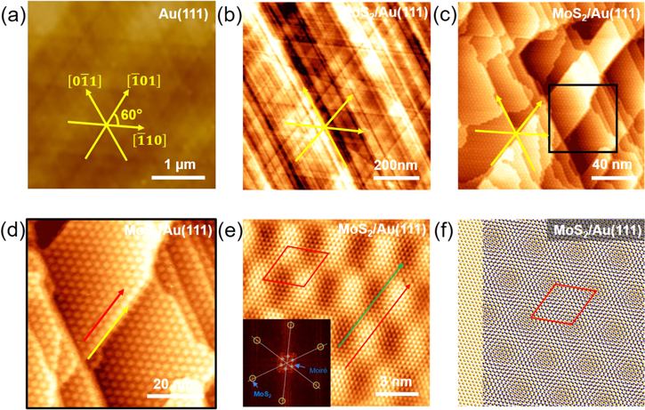
Figure 3. Monolayer MoS2 domains on the stepped Au(111) surface. (a) AFM image of the Au(111) surface, showing steps aligned along three directions (highlighted by yellow arrows) with a crossing angle of 60°. (b), (c) STM images (VSample = –0.01 V, ITunneling = 30.77 nA and –0.42 V, 3.44 nA) of the full-coverage monolayer MoS2 on the Au(111) facet, with the atomic steps of Au(111) clearly visible. (d) Magnified STM image (–0.30 V, 3.90 nA) of the black square region in (c), showing a hexagonal moiré pattern of MoS2/Au(111) with a period of ∼3.21 nm. The orientations of moiré pattern and Au(111) step are denoted by red and yellow arrows, respectively. (e) Atomically resolved STM image (–0.06 V, 12.64 nA) of MoS2/Au(111) presenting the perfect alignment of the orientation of the MoS2 lattice with the moiré row direction, as denoted by green and red arrows, respectively. Inset: the corresponding 2D-FFT pattern. (f) Simulation of moiré pattern for monolayer MoS2 stacking on Au(111) without relative rotation. The moiré supercell is highlighted by a red rhombus, corresponding to a (10 × 10) supercell of MoS2 as well as a (11 × 11) supercell of Au(111).
Download figure:
Standard image High-resolution imageAfter the growth of monolayer MoS2 triangular domains, as shown in the large-area STM image in figure 3(b), the bunched steps on Au(111) surface are well preserved. Although the steps seem to be straight and parallel on average, the magnified STM images (figure S4) indicate that, the atomic steps are locally meandering and consist of many short segments connected by kinks, the same as the references [39, 61]. This step morphology is very universal on the substrate surface since it can lower the free energy of the step [62–64].
After annealing the MoS2/Au(111) system at ∼400 °C for 10 h in the UHV chamber, the Au(111) surface becomes more smooth, presenting relatively large flat terraces separated by sparse steps (figure 3(c)). Further magnified image (from the region marked by black square in figure 3(c)) presents the evolution of large-area hexagonally shaped moiré pattern with a period of ∼3.21 nm (figure 3(d)). Notably, the orientation of the moiré pattern is well aligned along the direction of the Au(111) step, as highlighted by the red and yellow arrows, respectively. From the atomically resolved STM image in figure 3(e), the atomic lattices of MoS2 are observed with a measured interatomic distance of ∼0.320 nm. Moreover, the perfect orientation alignment of MoS2 atomic row with the moiré row is revealed, as denoted by green and red arrows, respectively, which is also confirmed by the corresponding 2D fast Fourier transform (2D-FFT) image (inset of figure 3(e)). Altogether, the atomic resolution STM images demonstrate an epitaxial relationship between monolayer MoS2 and the underlying Au(111) facet. As shown in figure 3(f), the simulation generated from non-rotated MoS2 monolayer on Au(111) presents a hexagonal moiré pattern with a period of ∼3.23 nm, which agrees well with the experimental data. Thus it can be determined that, the hexagonal moiré pattern mainly originates from the lattice mismatch effect between MoS2 (a1 = 0.320 nm) and Au(111) (a2 = 0.288 nm) rather than their relative rotation, according to the previous literatures for MoS2/Au(111) [65, 66]. Furthermore, the moiré supercell (highlighted by a red rhombus) is approximately corresponding to a (10 × 10) supercell of MoS2 as well as a (11 × 11) supercell of Au(111).
Notably, numerous STM characterizations focused on the edges of monolayer MoS2 domains show that, one edge of the triangular MoS2 domain is preferentially attached to the step edge of Au(111), which are highlighted by the representative STM images in figures 4(a) and (b). For more details, figure 4(c) presents a height profile analysis taken along the blue line (line ABC) in figure 4(b). Evidently, the height difference between B and C points is ∼0.20 nm, in line with the monatomic step height of Au(111). However, a larger height difference of ∼0.50 nm appears between A and B points, revealing the presence of a bunched Au(111) step (marked by black dashed line in figures 4(a) and (b)). In this regard, this MoS2 monolayer domain edge is attached to the bunched step of Au(111). The bunched step runs along the close-packed direction of Au(111), hereby the edge orientation of the MoS2 domain is also parallel to this substrate high symmetry direction.
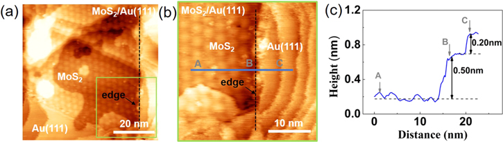
Figure 4. Observation of monolayer MoS2 domain attached to the step edge of Au(111). (a) Typical STM image (–0.54 V, 3.55 nA) showing one edge of the MoS2 triangular domain attached to the step edge of the Au(111) substrate. The edge is marked by the black dashed line. (b) Magnified STM image (–0.58 V, 4.29 nA) of the green square region in (a). (c) Height profile of MoS2/Au(111) taken along the blue line in (b).
Download figure:
Standard image High-resolution imageIt has been theoretically predicted that, the nucleation of 2D materials near a step edge is energetically more favorable than that on a flat terrace, due to its lower formation energy with the edge of 2D layers [38, 39, 67]. Such preferential nucleation behavior was also reported for the aligned growth of h-BN domains on the Cu(110) surface [25]. On this basis, the probable growth process for monolayer MoS2 on Au(111) is proposed as follows. At the initial stage, MoS2 preferentially nucleated along the step edge, rather than on the flat terrace of Au(111). Subsequently, under the guidance of both the step edge and the similar surface lattice symmetry of Au(111), monolayer MoS2 nuclei grew laterally to show larger domain sizes and two preferential domain orientations.
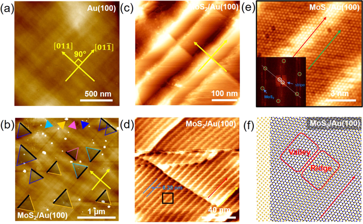
In addition, the orientation relationship between the MoS2 domains and underlying Au(100) was also investigated at the atomic scale. Different from the six-fold symmetric Au(111), the four-fold symmetric Au(100) surface shows bunched steps aligned along two perpendicular directions (marked by yellow arrows in figure 5(a)). As also evidenced by the high resolution STM image, the step edges are aligned along the close-packed directions of [011] and [01–1] of the Au (100) facet (figure S3(b)). After the CVD growth process, the MoS2 domains appeared to show mainly four orientations (highlighted by colored triangles in figure 5(b)) on the Au(100) surface. Intriguingly, one of the MoS2 domain edges (denoted by black lines) is always parallel to the step edge of Au(100) (marked by yellow arrows), similar with those on the Au(111) surface. Besides, the perpendicular steps underneath MoS2 are well preserved, according to the STM image in figure 5(c).
Figure 5. Monolayer MoS2 triangular domains on the stepped Au(100) surface. (a) AFM image of the Au(100) surface showing the steps aligned along two perpendicular directions of [011] and [01–1], as marked by yellow arrows. (b) AFM image of monolayer MoS2/Au(100) with one of the MoS2 domain edges (highlighted by black lines) aligning parallel to the Au(100) step edge (marked by yellow arrows). (c) Large-scale STM image (–0.31 V, 3.12 nA) of monolayer MoS2 on Au(100). The two perpendicular steps of the underlying Au(100) are visible (marked by yellow arrows). (d) STM image (–0.02 V, 7.85 nA) of MoS2/Au(100) showing a striped superstructure pattern with a period of ∼6.20 nm. The orientations of the striped pattern and Au(100) step are denoted by red and yellow arrows, respectively. (e) Atomically resolved STM image (–0.02 V, 11.86 nA) of the black square region in (d), revealing the MoS2 atomic row (marked by green arrow) aligning well with the striped pattern (marked by red arrow). Inset: the corresponding 2D-FFT pattern. (f) Simulation of the striped pattern formed by monolayer MoS2 stacking on the Au(100) lattice without relative rotation. The ridges and valley (bright and dark) regions of the striped pattern are highlighted by rectangles.
Download figure:
Standard image High-resolution image
According to the STM characterization of MoS2/Au(100) (figure 5(d)), a striped superstructure pattern is observed with a period of ∼6.20 nm between the adjacent stripes. According to the published reference, the typical striped superstructure is mainly due to the stacking of three-fold symmetric MoS2 on four-fold symmetric Au(100) and their lattice mismatch effect [68]. Moreover, the orientation of the striped superstructure is well aligned with the Au(100) step edge, as marked by red and yellow arrows, respectively. Further magnified STM image of the black square region in figure 5(d) indicates that, the MoS2 atomic row is also well aligned with the stripe direction of the superstructure, as denoted by the green and red arrows, respectively (figure 5(e)). Therefore, the lattice direction of the monolayer MoS2 is aligned along the direction of the stripe, or the close-packed direction of the Au(100) lattice. Besides, the corresponding 2D-FFT image of MoS2/Au(100) (inset of figure 5(e)) presents two types of spots for MoS2 lattice (green circles) and striped pattern (white circles), revealing the lattice alignment relationship between MoS2 and Au(100). Moreover, the structural simulation (figure 5(f)) by the parallel stacking of monolayer MoS2 on Au(100) is consistent well with the experimental result. Considering the four-fold symmetry of Au(100), there are four equivalent rotatory configurations of monolayer MoS2 domains on the Au(100) facet that can achieve the lattice alignment between MoS2 and Au(100), as schematically shown in figure 1(b).
Notably, the bunched steps prefer to form along the close-packed directions of Au(111) and Au(100) facets (i.e. [0–11], [–101] and [–110] for Au(111), [011] and [01–1] for Au(100)). Due to the existence of dangling bonds and defects, these step edges have higher binding energies and are more attractive to reactants than flat terraces [69], and therefore, the preferential nucleation of MoS2 occurs at the (bunched) step edges, resulting in the formation of oriented nuclei. In addition, according to the theoretical calculation [70], the binding energy between MoS2 and Au is 0.35 eV per unit, higher than that of interlayer MoS2 (0.23 eV per unit). The interface interaction between MoS2 and Au is stronger than the interlayer van der Waals (vdW) interactions in bulk MoS2, but not as strong as typical covalent bonding [70–73]. By exploiting the relatively strong MoS2-Au interaction, the MoS2 nuclei can be stabilized against decomposition and grow laterally. Eventually, monolayer MoS2 triangles are formed and tend to align with one of their edges along the close-packed directions of Au(111) and Au(100) facets, as dictated by the substrate symmetry and the presence of step edges.
4. Conclusion
In summary, the orientation-controlled growth of monolayer MoS2 triangular domains has been realized on different symmetric Au(111) and Au(100) facets by using the APCVD method. Triangular monolayer MoS2 domains on the six-fold symmetric Au(111) facet are unveiled to present two type orientations with rotation angles of 0° and 60°, whereas four type orientations on four-fold symmetric Au(100) facet showing 0°, 30°, 60°, 90° rotation angles. Moreover, with the aid of on-site STM technique, the orientation relationships between MoS2 and the different symmetric Au substrates are well established. Specifically, the edges of monolayer MoS2 domains are always aligned along the close-packed directions of either Au(111) or Au(100) substrates. Besides, the bunched steps are also formed along the close-packed directions of Au substrates, which are proposed to be responsible for the preferential nucleation of monolayer MoS2 at the initial nucleation stage. Note that MoS2 with predefined orientation can be applied to further explore specific merging behavior and physical/electrical properties of different MoS2 domains. Especially, the relative uniform orientation of monolayer MoS2 on Au(111) can dramatically decrease the existence of domain boundaries. The mono-orientation of monolayer MoS2 is also possible by further tailoring the CVD growth process from kinetic point of view. Briefly, this work should contribute significantly to understanding the substrate facet/step effects on the nucleation and orientation of monolayer TMDs, and provides valuable insights into the syntheses of large TMD single crystals for future device related applications.
Acknowledgments
The work was supported by the National Key Research and Development Program of China (No. 2018YFA0703700), the National Natural Science Foundation of China (Nos. 51991340, 51991344, 51925201 and 51861135201) and the Beijing Natural Science Foundation (No. 2192021).