

Abstract
Enhanced stability of a piezoelectric nanogenerator (PNG) was demonstrated using c- and m-axis GaN/V2O5 core–shell nanowires (NWs) by analyzing the capacitive coupling of the PNG's output. The NW array grown on GaN thin film was embedded in polydimethylsiloxane (PDMS) matrix, following which the matrix was transferred to an indium (In)-coated PET substrate for achieving superior flexibility of the PNG. The stability of the PNG was enhanced by holding the NW PDMS composite with a PDMS polymer as a bonding material on the PET substrate. The inserted PDMS layer improved the lifetime of the PNG, however, because of the insulating nature of PDMS, the piezoelectric output of GaN NWs was coupled capacitively to In contact on PET substrate and it resulted in a slight degradation of piezoelectric output due to the voltage drop across the bottom capacitive contact. The maximum piezoelectric current was 64 nA and output voltage was 11.9 V from the PNG with c-axis NWs. While the PNG with direct bottom contact exhibited 57% output reduction after 72 000 operation cycles, the PNG with capacitive contact did not show any degradation in stability even after 150 000 cycles.
Export citation and abstract BibTeX RIS
Introduction
A piezoelectric nanogenerator (PNG) is a mechanical-energy harvester that converts input mechanical energy to electricity. It can replace batteries in micro- and nano-devices because of its small footprint and low weight. In addition, it does not require periodic charging. Mechanical energy is abundantly available in our environment in various forms of motion such as human movements, wind, water flow, and sound waves. The efficient harvesting of mechanical energy in a wide range of frequencies is of great interest recently, and it is necessary to utilize flexible and stable piezoelectric materials to comply with vibration sources that have low amplitude and wide frequency range.
To meet the technological challenges while selecting a piezoelectric material, there are several other aspects that need to be considered. In the case of using ceramics as piezoelectric material, lead zirconate titanate (PZT) is one of the popular piezoelectric materials, but its poor biocompatibility due to toxic lead component limits its applications in medical nanodevices [1]. In this regard, semiconductor piezoelectric materials such as ZnO [2–4] and GaN [5–7], which are biocompatible and environmentally friendly, are actively investigated for developing PNGs. However, there is an inherent problem originating from the free carriers of a semiconductor-based PNG: screening of the piezoelectric field and the consequent degradation of the generated PNG output. Theoretical investigations based on the density functional theory show that ZnO has unintentional n-type conductivity due to interfacial charge traps and impurities [8, 9]; this conductivity enhances the free-carrier screening effect. Moreover, it is challenging to epitaxially fabricate ZnO pn-homojunction, which is essential for the formation of built-in potential and the suppression of junction current screening. Instead, GaN is more suitable for fabricating PNGs because of its high crystallinity and controlled n- and p-type conductivities [10].
The piezoelectric performance of GaN thin film (TF)-based PNGs is worse as compared with NW-based PNGs. Because of large lattice mismatch between GaN TF and sapphire substrate, Ga vacancies are favorably formed at the interface of GaN TF with the growth substrate [11]. Such kind of complications that are observed in bulk materials are avoided in case of GaN NWs because of strain relaxation (due to less coverage area of NW on substrate) between NWs and the growth substrate [12]. Furthermore, the single crystallinity and flexibility of GaN NWs enhance their applicability in self-powered electronics, and the lateral confinement of electron motion in GaN NWs reduces the free-carrier screening effect as well.
Regarding the fabrication of GaN-based PNGs, it was challenging to fabricate flexible PNGs as compared with rigid PNGs. The rigid PNGs [10, 13, 14] have limited applications due to lack of flexibility and stability. GaN TF-based flexible PNGs were fabricated by lifting–off GaN membranes via selective electrochemical etching [15, 16]. The maximum stability exhibited by GaN-TF-based flexible PNG was 800 cycles which was not enough to use it in many self–powered electronics where higher stability is needed. To demonstrate the potential of GaN-based PNGs as highly stable and high-performance energy harvesters, the GaN NWs were incorporated in the fabrication of flexible PNGs [17–19]. As discussed above, the GaN NWs have several advantages over GaN TF but their transfer from rigid to flexible substrate is a challenging task because of complicated lift-off processes. There are reports on manual peeling-off of the polydimethylsiloxane (PDMS) embedding NWs directly from the sapphire substrate [20, 21], but this technique is not successful enough because it leaves the residues of NWs on the rigid substrate. However, we fabricated the NW-based flexible PNGs using doctor blading technique which is the appropriate way to transfer the NW-matrix from rigid substrate. The maximum stability reported so far by the NW-based flexible PNGs was 36 000 cycles at frequency of 10 Hz [19], which was 45 times higher than the stability exhibited by TF-based flexible PNGs. However, during the repeated tests of GaN NW-based PNGs at high frequency, a marked drop in stability was later observed. The stability was degraded because of the mechanical damage of NWs due to direct NW-metal contact.
In this paper, we propose a simple and stable device design for the PNGs fabricated with c- and m-axis GaN/V2O5 core–shell NWs by fixing PDMS embedded NWs (NW-matrix) on a flexible substrate firmly with PDMS polymer layer. Because of the insertion of PDMS layer, the resulting capacitive coupling of piezoelectric power is designed for mechanical-energy harvesting. The measurement of piezoelectric characteristics and stability is performed on this PNG, and the effect of capacitive contact design is analyzed.
Experimental procedure
The PNGs were fabricated with c- and m-axis GaN/V2O5 core–shell NWs. The Au-catalyst assisted GaN NWs were grown on c-plane GaN TF by metal organic chemical vapor deposition (MOCVD) using the vapor–liquid–solid (VLS) growth technique. Prior to the growth of GaN NWs, the GaN TF was epitaxially grown on sapphire substrate using MOCVD. Trimethylgallium (TMGa) and NH3 were used as gallium and nitrogen sources. Initially, the GaN buffer layer was grown as seed layer on sapphire substrate for 130 s; the growth temperature was 640 °C and the NH3 and TMGa flow rates were 246 mmol min−1 and 66 μmol min−1, respectively. Subsequently, the GaN TF was grown at 1190 °C for 3240 s under the flow of TMGa (195 μmol min−1) and NH3 (424 mmol min−1).
For the growth of GaN NWs, a 0.7 nm thick Au film was evaporated on GaN TF using e-beam deposition. Two separate experiments were performed for the growth of c- and m-axis GaN NWs. The VLS growth of NWs was initiated by employing Au/In/Ga alloy catalyst which was fabricated by depositing a thin In-layer on Au coated GaN TF followed by the deposition of Ga-capping. The alloy catalyst was agglomerated in H2 environment for 700 s at 800 °C under the reactor pressure of 75 torr. The agglomeration conditions for the growth of c- and m-axis GaN NWs were same. Similarly, the growth temperature (825 °C), growth time (6000 s), and TMGa flow rate (37 μmol min−1) were also same for the growth of c- and m-axis GaN NWs. However, the reactor pressure and NH3 flow rate were different which were 50 torr and 4.5 mmol min−1 for c-axis GaN NWs and 60 torr and 6.7 mmol min−1 for m-axis GaN NWs, respectively. The NWs' length was approximately 3.5 μm both for the c- and m-axis orientations. Subsequently, 17 nm thick V2O5 shell was deposited using the RF magnetron sputter, and the detailed description of the deposition process can be seen in our preliminary report [19]. The core–shell NWs were then encapsulated in PDMS with optimized coating conditions followed by dry etching to remove the PDMS from the top of the NWs. Subsequently, Ni/Au (15/200 nm) was coated as a top contact on the top of the core–shell NWs by using an e-beam evaporator. Meanwhile, a flexible bottom substrate was fabricated by evaporating 4.5 μm indium TF on a PET membrane using e-beam deposition, and this is referred to as 'bottom substrate' in the following text. Prior to the transfer of NW matrix, a thin layer of PDMS (5 μm) was spin-coated on the bottom substrate as a bonding epoxy for 300 s at 7000 rpm. The NWs embedded in the PDMS matrix (NW-PDMS composite) were separated from the GaN TF by using the doctor blading technique [19]. Furthermore, the bottom substrate was spin coated with PDMS for holding the NW-PDMS composite, and the whole structure was baked for 600 s at 150 °C. The PDMS layer on the bottom substrate enhanced the bonding between the NW-PDMS composite and the substrate. The top contact was formed on V2O5-coated GaN NWs with Ni/Au, while the bottom side of the GaN NWs has capacitive contact due to PDMS layer on In-coated PET substrate. The fabricated PNG's dimension was ∼1 × 1 cm2. The PNG based on c-axis GaN/V2O5 core–shell NWs is referred to as PNG-c, while the PNG based on m-axis GaN/V2O5 core–shell NWs is referred to as PNG-m. Figure 1 depicts the conceptual design of PNG-c with PDMS layer between NW-PDMS composite and the bottom substrate along with the layered structure of the PNG.
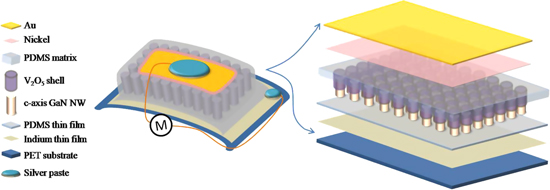
Figure 1. Schematic of PNG with capacitive contact and its layered structure.
Download figure:
Standard image High-resolution imageThe fabricated PNGs were installed in a mechanical actuator that periodically stretched and released the PNGs at different actuation frequencies [18]. The piezoelectric performances of the fabricated PNGs were characterized using a potentiostat/galvanostat/ ELS analyzer (PARSTAT 3000, Princeton Applied Research).
Results and discussion
The morphology and uniformity of the fabricated c- and m-axis GaN/V2O5 core–shell NWs were analyzed using scanning electron microscopy (SEM) and transmission electron microscopy measurements. The SEM images of the respective NWs after V2O5 deposition are depicted in figures 2(a) and (c). The c-axis GaN NWs were observed to be vertically aligned to the growth substrate, and they showed cylindrical morphology with uniform diameter. The NWs' diameter was approximately 60 nm after V2O5 deposition. However, the m-axis GaN NWs were observed to be tilted with respect to the substrate, and they showed tapered morphology. The conformal shell deposition of V2O5 on the c- and m-axis GaN NWs can be observed in figures 2(b) and (d), respectively.
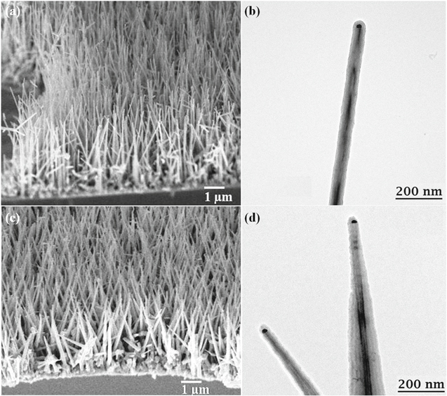
Figure 2. (a), (c) SEM and (b), (d) TEM images of GaN/V2O5 core–shell NWs. (a), (b) c-axis and (c), (d) m-axis NWs were characterized.
Download figure:
Standard image High-resolution imageAfterward, the NWs were fabricated into flexible PNGs with PDMS as a bonding layer. The piezoelectric performance of the fabricated PNGs was measured at different actuation frequencies. Figure 3(a) depicts the piezoelectric output current of PNG-c under actuation frequencies of 4, 6, 8, and 10 Hz. At 4 Hz, the short-circuit current was 12 nA, and it increased to 32 nA at 6 Hz, 52 nA at 8 Hz, and 64 nA at 10 Hz. Figure 3(b) depicts the output current exhibited by PNG-m under the same frequency range from 4 to 10 Hz. The maximum output current exhibited by PNG-m at 10 Hz was 47 nA, which was lower than the current exhibited by PNG-c at the same frequency.

Figure 3. (a), (b) Piezoelectric output current and (c), (d) voltage of PNGs with capacitive contact at different actuation frequencies, (a), (c) was from PNG-c and (b), (d) from PNG-m.
Download figure:
Standard image High-resolution imageThe voltage responses of the fabricated PNGs were evaluated at different actuation frequencies ranging from 4 to 10 Hz. The maximum open-circuit voltages exhibited by PNG-c and PNG-m at 10 Hz were observed to be 11.6 and 7.8 V, respectively, as depicted in figures 3(c) and (d). The piezoelectric output exhibited by PNG-c is greater than the piezoelectric output exhibited by PNG-m because of high piezoelectric coefficient of c-axis GaN NWs. Moreover, unlike piezoelectric output current, the amplitude of the output voltage peaks does not depend upon the actuation frequency. The change in the actuation frequency does not generate new piezoelectric charges, but it fastens the piezoelectric polarization process, which, in turn, increases the drift velocity of free carriers.
When PNGs are bent in the concave downward direction, the NWs embedded in PDMS matrix experience different forces depending on the NWs' alignment inside the PDMS matrix. For PNG-c, the NWs are vertically aligned inside the PDMS matrix. Therefore, upon bending the PNG, the NW-PDMS composite stretches laterally, thereby causing compressive force in the normal direction. As a result, the embedded c-axis NWs experience uniform compressive stress on the top plane and tensile stress on their side walls, resulting in the generation of piezoelectric polarization along the c-axis. In the case of PNG-m, the NWs inside the PMDS matrix are tilted with respect to the bottom substrate. Therefore, during the bending, the NW-PDMS composite shows the same behavior as discussed above (i.e. lateral stretching); however, the PDMS-embedded m-axis NWs experience shear stress due to their tilted orientation. Consequently, the shear stress elongates the NWs, thereby resulting in the generation of piezoelectric polarization along the m-axis.
The generation of piezoelectric output from GaN/V2O5 core–shell NWs is discussed for PNGs that have capacitive contact with the help of an energy-band diagram, as depicted in figure 4. Moreover, the operation principle is compared to a PNG with direct contact. The PNG with direct contact is a PNG device with the same structure except it does not have the bonding PDMS layer; therefore, in a PNG with direct contact, the charge flows directly from NWs to In metal contact. The work function of In metal is 4.09 eV, while the electron affinities of GaN and V2O5 are 4.5 and 2.4 eV, respectively, as depicted in figure 4(a). When NWs are compressed vertically, positive and negative piezoelectric charges are generated, respectively, at the top and bottom sides of GaN NWs. With respect to the PNGs with capacitive contact (i.e. with PDMS bonding layer), the band bending and equivalent charge distribution across the capacitive contact and GaN-V2O5 interface is analyzed. Upon the generation of piezoelectric charges by applying stress, the resulting piezoelectric polarization induces the electric field inside the GaN region and bends the energy bands accordingly. Subsequently, free carriers are drifted on the opposite ends of GaN NWs under the induced piezoelectric field. The drifted carriers, then, establish an electric field that screens the piezoelectric field in the neutral GaN region. In this way, free electrons move to the edge of the GaN depletion region and, therefore, reduce the depletion region's width. However, the negative piezoelectric charges at the bottom side of GaN NWs are not fully screened because of the capacitance in the GaN/PDMS/In structure. Figure 4(b) depicts the energy-band bending and the corresponding charge distribution after the free-carrier screening. It is clearly presented that Fermi level in n-GaN is higher than that in p-V2O5 on the basis of the modified depletion region from the thermal equilibrium. This is the origin of piezoelectric voltage, when the piezoelectric medium is a conductive semiconductor.
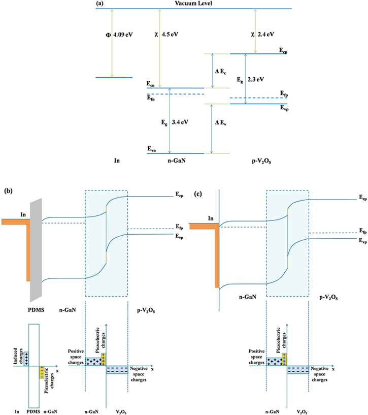
Figure 4. Energy-band diagram of PNG with respect to (a) vacuum level, (b) energy-band bending under compressive stress and the respective charge distribution across bottom contact and GaN-V2O5 interface for PNG with capacitive contact, and (c) energy-band bending and electric charge distribution across the GaN-V2O5 interface for PNG with direct contact.
Download figure:
Standard image High-resolution imageThe GaN/PDMS/In structure works as a charged capacitor with capacitance C = εA/d, where ε is the dielectric constant, A the device area, and d the PDMS thickness. Therefore, the voltage drop across the PDMS layer is directly proportional to the charge accumulation at the GaN-V2O5 interface. In this regard, the output voltage from the PNG with capacitive contact is degraded from the actual value of GaN/V2O5 core–shell NW. In addition, the energy-band bending and charge distribution in the PNG with direct bottom contact is depicted in figure 4(c). Overall, the mechanisms for piezoelectric polarization and drift of free carriers are the same as discussed above, except the charge carrier transportation through the bottom contact. There is no voltage drop at the bottom contact because the capacitance is negligible due to ohmic contact.
The analysis based on energy-band bending is in good agreement with the piezoelectric performance presented in figure 3. The piezoelectric performance of the PNG with direct contact was shown in our previous publication [19], and it was compared with the performance of the PNG with capacitive contact. The piezoelectric output of the PNG with capacitive contact was observed to be relatively reduced because of the dielectric PDMS bonding layer. The PDMS bonding layer provides additional capacitance because the generated piezoelectric charges in GaN induce opposite charges on the other side of the PDMS layer (In metal layer). The additional capacitance degrades the piezoelectric output. Moreover, epoxy material for firm bonding of NWs is essential for highly stable PNGs. Therefore, the piezoelectric performance and stability should be compromised in a proper way.
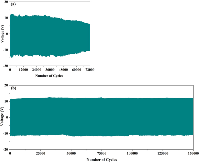
Because the effect of the PDMS bonding layer on the PNG's stability is of great concern, we tested PNG-c's both with capacitive contact and direct contact for comparison. For the PNG with direct contact, the device was fabricated without PDMS bonding layer, and m-axis GaN/V2O5 core–shell NWs were incorporated. So, the electrical connection of NWs to the bottom substrate was obtained by mechanical contact. Both the PNGs were installed in a bending-releasing actuator operating at 10 Hz, and their stability of piezoelectric voltage output is depicted in figure 5. The PNG with direct contact displays a gradual degradation in stability after 36 000 cycles, as depicted in figure 5(a). Finally, the output voltage dropped to 57% of the initial output after 72 000 cycles. The drop was attributed to the lack of proper bonding between the NW matrix and the In-coated PET substrate, so the damage of the bottom of NWs from mechanical friction is the primary cause of degradation. However, PNG with capacitive contact did not show significant degradation of the piezoelectric output voltage even after 150 000 cycles, as depicted in figure 5(b). As discussed earlier, the inserted PDMS layer between the NW matrix and the bottom substrate played a vital role in improving the lifetime of the PNGs. We believe that the piezoelectric output can further be enhanced by controlling the thickness of the PDMS layer and bottom PET substrate.
Figure 5. Stability test of PNGs (a) with direct contact and (b) with capacitive contact. The test was performed using a mechanical actuator at 10 Hz.
Download figure:
Standard image High-resolution image
Conclusion
It is challenging to fabricate semiconducting NW based flexible and stable PNGs for real-life applications. The c- and m-axis GaN NW arrays were grown on a GaN TF; however, for achieving enhanced flexibility for the PNG, transferring the NWs to a flexible PET substrate was a challenging task. The superior flexibility of PNGs was achieved by transferring the GaN/V2O5 core–shell NW arrays from GaN TF to the flexible PET substrate by using the doctor blading technique. For achieving enhanced stability of PNGs, a thin PDMS layer was used as an epoxy material for bonding the NW arrays with bottom substrate. Compared with PNGs fabricated with direct bottom contact, the PNGs with capacitive contact did not show any degradation in stability even after 150 000 cycles. This stability is attributed to the firm bonding of NWs with the bottom substrate. However, the PNGs with capacitive contact showed a slight degradation in piezoelectric output due to the voltage drop across the bottom capacitive contact. Therefore, the PNG with capacitive contact exhibits superior stability and reasonable piezoelectric output, and its biocompatibility makes it a promising candidate for in vivo medical applications.
Acknowledgments
This work was supported by the National Research Foundation of Korea Grant funded by the Korean Government (NRF-2019R1A2C1006360).