

Abstract
In this work, we use Joule-effect thermal evaporation to produce hybrid structures made of Ga and In nanoparticles (NPs) on Si (100) substrates. Taking advantage of the protective oxide shell, In NPs can be used as a template for a second deposition step without structural changes, enabling the hybridization of NPs of materials. These complex structures of mixed NPs present a spectrally broad plasmonic absorption that can be optically tuned with a wide range of photon energies from UV to IR regions with a full width at half maximum range of ∼400 to 800 nm. The results suggest that the localized surface plasmon resonance (LSPR) of the hybrid NPs is mainly due to the plasmonic coupling of the in-plane modes. Furthermore, different scenarios studied by discrete dipole approximation simulations show that the interconnection between NPs is extremely sensitive to the size and the local arrangement of the nanostructures. This kind of broadening and tunable LSPR may have interest for energy transfer applications, biosensing platforms and solar cells.
Export citation and abstract BibTeX RIS
1. Introduction
In the last decades, plasmonics has attracted a great deal of attention due to the powerful way to incorporate optics into nanoscience and nanotechnology [1, 2]. The principle is based on the manipulation of light as a result of the interaction with the collective oscillation of the free electrons. When this interaction occurs with metallic nanoparticles (NPs) the light is confined in the vicinities of them showing a strong oscillation mode called, localized surface plasmon resonance (LSPR). The surface plasmon (SP) energy is proportional to the resonance frequency of the oscillation and can be modified depending on the permittivity of the metal, particle size, shape and the surrounding medium [3, 4].
Typically, noble NPs such as Au and Ag have played a leading role in many studies, with their tunable LSPRs in the visible and infrared (IR) regions [4–8]. More recently, studies using nanostructures composed of poor metals such as In, Ga, Cu or Al show that this range can be extended from the ultraviolet (UV) to the IR spectrum [7, 9–13]. Moreover, the optimization and the enhancement of the electric field associated with the LSPR can be achieved by designing structures that have an inhomogeneous configuration, such as core–shell particles [1, 5, 14, 15] or by hybridization of the individual plasmon resonance [16, 17]. However, most of the studies related to the plasmon hybridization are based on theoretical calculations [18–22]. Calculations based on the electrodynamic theory of two adjacent NPs show that the near-field enhancement depends on the NP–NP hot-spot interaction and on the polarization of the incident light [22, 23]. On the other hand, the hybridization model indicates that the plasmon coupling between complex nanostructures can be understood in terms of interaction between the plasmon modes of the individual NPs [20, 24]. Both models contribute to the fundamental understanding in the application in plasmonics, such as the possibility to tune the resonance wavelength in a wide spectral range by varying the distance between particles, or by combining complex nanostructures.
Among the plasmonic nanoparticles used up today, those made of Ga and In are good candidates for UV plasmonics because of their resistance to oxidation at ambient conditions beyond their natural thin oxide-shell layer (∼2 nm) that has been demonstrated slightly affect its optical properties [25–27]. In particular, Ga is a material with low toxicity and low viscosity and such properties offer advantages to be used as a platform in biosensors and bioelectronics [28, 29]. More recently, has been reported that the use of Ga NPs induces a photoluminescence enhancement of 2D monolayer MoS2 [30]. Indium NPs has also potential applications in biotechnology (as tags for electrochemical detection of DNA hybridization) and due to its physical properties in nanoelectronics (for single-electron transistor) [31, 32]. On the other hand, when In and Ga NPs are exposed to the atmospheric environment, a typical thin oxide-shell is formed about 2 nm in thickness [14, 33]. In particular, the thermal stability and the influence of the Ga2O3 shell thickness on the plasmonic properties at low temperatures (RT–300 °C) and up to 900 °C have been studied by our group in the past [15, 27]. The results from these studies open the possibility of tuning the plasmon resonance in a wide range of temperatures without affecting the optical properties significantly. Moreover, we show an easy and effective method to control the liquid Ga–Ga2O3 ratio by thermal treatments and NPs radius. Thanks to this thin oxide layer is possible to create mixed nanostructures avoiding the eutectic Ga-In (EGaIn) formation [34]. Despite the advantages of the promising plasmonic properties of these materials, there is a scarcity of studies combining both elements.
In this paper, we investigate the hybridization of Ga and In NPs with the aim to spectrally broaden the absorption range, that can improve the performance in solar cells or energy transfer applications [35, 36]. We will explore the possibility to tune the LSPR from UV to IR range avoiding the miscibility of both materials.
2. Methods
Hybrid nanostructures composed of Ga and In NPs have been prepared by Joule-effect thermal evaporation using a vertical Edwards E306 system. The evaporation was carried out in a high vacuum chamber with a base pressure of 2 × 10⁻⁷ mbar. The hybrid nanostructures are obtained in two steps: by depositing first, In (99.99999% purity) on the substrate and immediately after, Ga (99.9999% purity). The size of the NPs are limited by the amount of In or Ga used, thus, different amount of metal masses were used in order to find the optimal plasmon resonance. The filament (tungsten 99.90% purity) power during the evaporation process was set to 40 W in case of In and 50 W in case of Ga, and the working pressure was 1.5 × 10⁻⁵ mbar. The substrate-metal-source distance and the duration of the evaporation process were kept constant at 200 mm and 60 s, respectively. The substrate used in this work was Si (100) one-side polished.
The morphology characterization of the In, Ga NPs and the hybrid system was imaged by means of field-emission scanning electron microscopy. The microscope is a FEI XL30-SFEG system, operating with 10 keV electron beam and nominal lateral resolution of 4 nm, being the secondary electrons collected and analysed with an Everhart-Thornley detector. The morphology characterization determined by SEM will be essential in order to create the nanostructures for discrete dipole approximation (DDA) simulations.
The optical properties of the samples were analyzed by means of spectroscopic ellipsometry (SE), using the M-2000® system from JA Woollam Co in the wavelength range from 210 to 1680 nm (5.90–0.74 eV). The measurements were taken in external reflection configuration at 70° incidence angle referred to the normal of the sample surface. The samples were illuminated with a light beam linearly polarized at 45º then, and after reflection from the sample surfaces, the change in the polarization state of the light beam was measured. The change in the polarization state characterized by the ellipsometric parameters psi (ψ) and delta (Δ) [37] is defined in the next equation:

where ρ is is a complex number defined as the ratio of the reflectivity for p-polarized light (rp) divided by the reflectivity for s-polarized light (rs). The ellipsometric parameters report this value in polar form where tan(Ψ) is the magnitude of the reflectivity ratio, and Δ is the phase. Finally, the pseudo-dielectric constants  of the sample can be obtained from the analytic transformation:
where  is the angle of incidence and ρ was defined in equation (1). The pseudo-dielectric function can be directly displayed of the current SE data with the CompleteEASE software from JA Woollam Co. More information about the ellipsometry applications for plasmon resonance characterization can be found in [38].
In order to analyse the plasmon resonance coupling of the In-Ga hybrid NPs, we evaluated the light particle interaction with the DDA code DDSCAT 7.2 [39]. As it has been demonstrated previously, there is a good match between experimental results for a large number of particles and with DDA simulations of isolated nanoparticle [14, 15, 27]. The enhancement of the electric field is simulated in both modes in-plane (parallel to the plane of incidence) and out-of-plane (perpendicular to the plane of incidence). The illuminating beam is a monochromatic linearly polarized plane wave with polarization ( ) perpendicular to the propagation (
 ) direction. The extinction efficiency (Qext) is calculated from the DDA simulations and the wavelength used for evaluating the electric near field is chosen where the Qext is maximum. The DDA simulations does not include the substrate in order to speed up the calculation time and to avoid introducing changes when they stand on a dielectric surface [26, 40]. Thus, we infer the results only from the interaction from the electric field between NPs. The nanostructures were created by a target generation tool program executed by Matlab [41]. These targets were discretized into arrays of N polarizable points with polarizabilities deployed on a cubic lattice following the same parametrization than in [27]. Calculations of the Qabs, Qscat and Qext efficiency were carried out using a dipole lattice spacing of 2 nm to ensure a number of dipoles higher than 100 000, achieving a good description of the target geometry by this method. For more information about the size parametrization, consult the [27]. The input dielectric properties of liquid Ga and In were taken from the literature [42–44].
3. Results and discussion
3.1. Individual non-hybridized NPs
In order to investigate the coupling of the LSPR, we have evaporated different masses of Ga and In NPs. Firstly, different In NPs with different sizes were evaporated on bare Si (100) substrates, with masses ranging from 25 up to 100 mg. Secondly, Ga NPs were evaporated on these samples with the aim of creating a hybrid system. The natural oxidation of the In NPs when they are exposed to air avoids the formation of the eutectic gallium-indium alloy [45]. Each evaporation process was carried out simultaneously on Si substrates, used as reference samples prior to the hybridization. The morphology of the as-grown structures on Si was characterized by SEM and their LSPR measured by SE (figure 1).

Figure 1. Top-view and cross-sectional (in the inset) SEM images of (a) In and (b) Ga NPs on Si substrates. On the right, the figure shows the SE spectra for different masses (c) of In and (d) of Ga NPs. The dot black line corresponds to 25 mg, the dashed red line corresponds to 50 mg and the blue line corresponds to 100 mg.
Download figure:
Standard image High-resolution imageFigure 1(a) shows faceted nanostructures corresponding to the In NPs while figure 1(b) shows the round shape of the Ga NPs. Additionally, the cross-sectional images are shown in the inset. Indium facets reveal the formation of a crystalline phase after the growth. The NPs are formed by a coalescence mechanism and, for very long evaporation process, this can lead to a uniform thin layer [46]. On the other hand, Ga is a liquid metal at room temperature, and when it is evaporated on Si tends to form liquid droplets. Due to the surface tension and surface mobility, the droplets can coalesce together and form bigger NPs with a hemispherical shape. Therefore, for long times the evaporation of Ga results in a bimodal distribution of NPs [27] but rarely can lead to a thin film.
The figures 1(c) and (d) show the imaginary part of the pseudodielectric constant 〈ε2〉 obtained by SE measurements for different masses 25, 50 and 100 mg of In and Ga NPs, respectively. These curves represent the intensity of the LSPRs versus the wavelength and energy due to the interaction between the light and the NPs. Moreover, as we can observe from the cross-sectional SEM images (insets in the figures 1(a) and (b)), both Ga and In NPs exhibit a clear different aspect ratio between vertical and longitudinal axes. Thus, results in two different resonance modes, which are visible in the spectrum form figure 1 with two dominant peaks: the out-of-plane and the in-plane [25]. In SE spectrum, the out-of-plane LSPR mode is only visible for bigger particles (larger masses, 100 mg) in the range of 200–300 nm. However, if the particles are big enough, the peak in the shortest wavelength region could be result affected for the contribution of high order LSPR. In this case, separate the two effects results very difficult. The in-plane LSPR mode redshifts toward the longer wavelength (from 400 to 1200 nm) with the increases masses. The resonant wavelength increases as the particle size increases showing a dependence of the spectral position of the LSPR [47]. These results are in agreement with those reported in the literature [25, 48].
3.2. Hybrid NP system
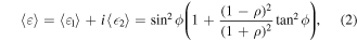
As shown previously the size of the NPs is directly correlated with the optical absorption, but an additional way of tuning the plasmon resonance is by coupling between different particles [1], which is studied here. Taking advantage of the flat surface of In, the In islands can be used as a substrate for a second deposition step without structural changes for Ga NPs. Thus, the Ga NPs can be accommodated easily on top. In addition, the resistant oxide shell of the Ga NP makes the liquid Ga stable at room temperature permitting the formation of the hybrid system [14, 15, 27]. To see how the plasmonic coupling changes with the particles size we have studied two cases: (i) we have fixed the Ga mass (25 mg) evaporated on different masses of In (25–100 mg) and (ii) we have evaporated different masses of Ga (25–100 mg) on a fixed mass of In (25 mg). During the hybridization process, some of the Ga particles will remain in the upper part, which enables coalescence and the formation of bigger particles. Other Ga NPs will stay surrounding the In NPs, grown on the empty spaces between In islands. The results of the different conditions (i) and (ii) are shown in figures 2 and 3 respectively.
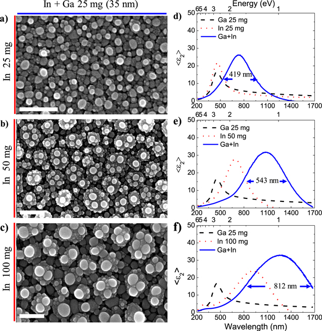
Figure 2. From (a) to (c) SEM images of In-Ga hybrid system: 25 mg of Ga deposited on different masses of In (a) 25 mg, (b) 50 mg, (c) 100 mg. The scale bar in all images is 200 nm. From (d) to (f) the results of SE measurements for each sample. The FWHM of In-Ga hybrid system is also depicted in the plots.
Download figure:
Standard image High-resolution image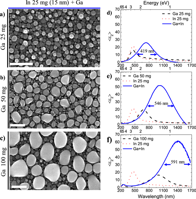
Figure 3. From (a) to (c) SEM images of In-Ga hybrid system: different masses of Ga (a) 25 mg, (b) 50 mg, (c) 100 mg deposited on 25 mg of In. The scale bar in all images is 200 nm. From (d) to (f) the results of SE measurements for each sample. The FWHM of In-Ga hybrid system is also depicted in the plots.
Download figure:
Standard image High-resolution imageFigure 2(a)–(c) show the SEM images for a fixed mass of Ga (25 mg) deposited on different masses of In (from 25 to 100 mg). For minor masses (figure 2(a)), the coalescence of Ga on top of the In islands is small and, thus, the radius of Ga is similar to the size of the In beneath. When the mass of In increases (figure 2(b)), more Ga NPs can be deposited on top of In islands, and this effect increases the coalescence and results in a higher density of Ga NPs per In islands. Simultaneously, Ga nanoparticles start to fill the flat regions between In islands, where the coalescence mechanisms also take place. Finally, for large In masses (figure 2(c)), the accessible area on top of the islands for the interaction between Ga NPs is larger and therefore the particles continue coalescing. On the contrary, the space between islands is reduced, so that Ga particles growth directly on the bare Si substrate tend to form bridges connecting the In particles between them. The SE measurements from the hybrid samples are shown in figures 2 (d)–(f) together with the SE from In and Ga samples as references. In all the hybrid samples, the plasmon resonance is more intense (reaching a maximum value of 33 in figure 2(f)) than the reference values and redshifts are due to the hybridization process. The resulting resonances from the hybridization are located in the red-IR region at 739, 1074 and 1246 nm, respectively. The redshift can be understood as a consequence of the overall increase of the plasmonic structures, as it happens with individual NPs when increasing the size (figure 1). A remarkable feature of the combined LSPR is that the FWHM increases with the increasing size of the In islands. Therefore, the broadening of the LSPR can be tuned from 419 nm up to 812 nm covering a wide range of the spectrum. This fact is due to the wider resonance of In islands for large masses, but also to the coupling with the Ga NPs deposited, as we will discuss later on.
Figure 3(a)–(c) show the SEM images for different masses of Ga (from 25 to 100 mg) deposited on a fixed mass of In (25 mg). In this case, the size of the In islands is quite small compared to the size of the Ga NPs. The Ga NPs can coalesce in the empty region between the In islands and few of them on top, forming bigger Ga NPs. This is possible because the coalescence of Ga is very fast, leading to form big coverings of Ga over the In NPs (see figures 3(b) and (c)). When greater masses of Ga are evaporated, the NPs form a leaf-like shape that can cover the In particles, which affect the surface tension of the resulting NPs, leading to a loss of their hemispherical shape. Thus, In islands lie buried underneath the Ga NPs. The corresponding pseudodielectric function for every particular system is shown in figures 3(d)–(f), together with the In and Ga spectrum references. The position for the hybrid LSPR changes with the Ga mass, resulting in peaks in the red-IR region: at 739, 1032, and 1400 nm, respectively. The FWHM of the plasmon resonance from the hybrid In-Ga (indicated in the figure 3) increases with the Ga mass from 419 to 591 nm. Moreover, the plasmon resonance becomes more intense for the hybrid NPs reaching the maximum value at 62 (see figure 3(f)).
As has been shown, we have two different ways to couple the LSPR of Ga and In. With the first system (figure 2) we get broader plasmon resonance and with the second system (figure 3), we get more intense plasmon resonance. The main difference between both systems (figures 2 and 3) is the coalescence of Ga NPs. In the first system, the coalescence of Ga NPs is limited by the In islands and therefore the size is controlled by the available area on top of the In islands and in the empty regions between the In NPs. This mode of coalescence favors the LSPR broadening by increasing the FWHM up to 812 nm. However, in the second case, the In NPs are so small that Ga NPs can coalescence without boundaries, leaving In NPs buried, and affecting the surface tension and the shape of the NPs. The Ga NPs lose the sphericity and likely the contribution of In NPs becomes negligible to the LSPR broadening, although this mode of coalescence favors the intensity because the NPs are very large. In both cases, the LSPR after the hybridization experiences a redshift accompanied by a broadening and an increase in the intensity.
3.3. DDA simulations
The main cause for the observed effects of the hybridization process is the plasmonic coupling of both Ga and In NPs as occurs with other systems formed by spherical or complex nanoparticles [18–20, 49]. In order to investigate this coupling from a theoretical point of view, we have carried out DDA simulations, as mentioned in the experimental section. Firstly, we have performed DDA simulations of individual In and Ga NPs, and secondly, we have analyzed the interaction between the NPs (laterally or vertically).
In figure 4 we show the local electric field distribution for two representative sizes (∼80 nm in diameter) of an In (a) and a Ga (b) NP. The enhancement of the electric field has been simulated in both modes, in-plane (parallel to the plane of incidence) and out-of-plane (perpendicular to the plane of incidence). The polarization ( ) and the propagation (
 ) of the light beam direction are indicated in the figure. The wavelength used for evaluating the electric near field corresponds to the maximum of the LSPR is also indicated. The interactions between the oscillating electric field of the light and the surface charges are strongly dependent on the shape of the NPs [1]. It can be seen in the figure that the enhancement of the electric field increases in the in-plane mode for In, being more intense in the corners due to the flat disc shape. The maximum of the relative intensity in this case is 11. For Ga is the opposite, and the electric field increases in the out-of-plane mode reaching a maximum enhancement value of 18. This can be explained due to the hemispherical shape of the particle [27].

Figure 4. The local electric field distribution in-plane and out-of-plane, for individual nanoparticles of (a) In and of (b) Ga. The wavelength used for evaluating the electric near field corresponds to the maximum of the LSPR is indicated in all figures.
Download figure:
Standard image High-resolution imageIn order to study if the hybridization effects induce an enhancement of the LSPR, in both the near- and far-field regimes, we have analyzed the interaction between two or more particles. As we have seen in the SEM images, the interaction can be due to horizontal or to vertical coupling, since Ga NPs can be on top or at the side of the In islands. We have evaluated the enhancement of the near electric field on different NPs size but here we focus only on the NPs that better represents the experimental results. Figure 5(a) schematically illustrates a picture of the hybridization process, which consists of some Ga particles around In and some on top of the In surface. We have calculated the enhancement of the electric field by DDA simulations in both cases, (i) one NP of Ga next to the In NP and (ii) one NP of Ga on top of In NP. The results are shown in figures 5(b)–(e) respectively. In both scenarios, we have considered the coupling between the in-plane and the out-of-plane modes of each NPs by changing the polarization mode of the incident light.
Figure 5. (a) Schematic picture of the hybridization process: the In NPs (red rectangles) are evaporated first and secondly Ga NPs (black hemisphere) on top and surround In. (b) to (e) DDA simulations of the hybrid system. (b) Local electric field distribution in-plane for the hybrid system when Ga is next to In and (c) the calculated Qext for this hybrid configuration (blue line) together with In (red line) and Ga (black line) as references. (d) Local electric field distribution for the hybrid system when Ga is on top of the In, and (e) the calculated Qext for this hybrid configuration (blue line) together with In (red line) and Ga (black line) as references. The wavelength used for evaluating the electric near field corresponds to the maximum and high-ordered LSPR is indicated in figures (b) and (d).
Download figure:
Standard image High-resolution imageIn figure 5(b), when one particle is next to the other, the maximum enhancement of the electric field occurs at 610 nm for the in-plane polarization mode (parallel to the surface interparticle contact) and a hot-spot is formed in the space between NPs. This happens when the In and Ga particles are sufficiently close to each other, i.e. the distance between them should be within the decay length of the electromagnetic field associated with the mode. Further simulations (not shown) varying the distance between particles have shown that intense hot-spot occurs when the NPs are separated around 1 nm. In figure 5(d), when one particle is on top of the other, the enhancement of the electric field occurs at 310 nm through the coupling of the out-of-plane modes (perpendicular to the surface interparticle contact) and not between the in-plane modes. In order to analyze these results in the far-field regime, we have considered the calculated Qext from the simulations, which takes into account both scattering and absorption optical efficiencies and is defined as the ratio between the cross-section of the NP and its geometrical cross-section [50]. In the SE measurements, the incident beam suffers scattering and absorption losses upon the reflection on the sample surface. Therefore, Qext is the most suitable parameter to compare with the experimental results. The resulting Qext from the simulations for both structures are shown in figures 5(c) and (e) respectively. The Qext from the hybrid systems are represented together with Ga and In NPs as references. As we can observe, there is a redshift and broadening in the LSPR for both hybrid configurations, although is more significant for the adjacent NPs (see figure 5(c)). The optical response of this nanostructure can be understood as a coupling of the plasmons of the individual nanoparticles [18]. If we evaluate the peaks in the UV region (200–250 nm), when one particle is next to the other (see figure 5(b)), the results from the simulation indicate the existence of two non-centered hot-spots weaker than the one at 610 nm. This fact can attributed to the second order dipolar resonance. However, when one particle is on top of the other (figure 5(d)), the enhancement of the near electric field seems to be more related to In than to the coupling effect. This is evidenced by the intense electric field in the border of the In disk, which is a signature of the dominant In resonance mode. Indeed, the peak wavelength at 214 nm of the hybrid system matches with the resonance peak of the isolated In particle, which is also very intense.
In order to analyze the position and the intensity associated with the LSPR coupling, we have varied the sizes of the NPs in both configurations. Figure 6 shows the local electric field distribution and the Qext analysis when Ga NP is next to In NP. In this case, we have kept constant the size of Ga NPs at 60 nm in radius, while In NPs were varied from 25 to 100 nm. The results indicate that the optimal value of the in-plane LSPR coupling is when Ga and In NPs have similar dimensions. The reason for this is that there is an optimum NP size for the Qext. This parameter reflects the contribution of the absorption (Qabs) and the scattering (Qscat) from the NPs. The Qabs is more important for big NPs while the Qscat is relevant for small NPs, thus a compromise between both contributions is achieved for intermediate sizes. As we can observe in figure 6(a) the hot spot is located between the two NPs, where the enhancement of the electric field is maximum. In the Qext analysis of figure 6(b) it can be observed how the LSPR intensity is optimized when the In and Ga NP have similar sizes.
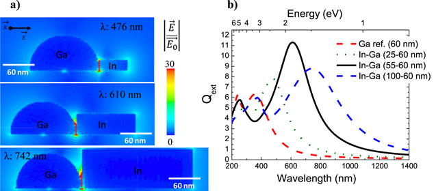
Figure 6. DDA in-plane simulations for the hybrid system Ga next to In. Figure (a) shows the geometry of the NPs and the local electric field distribution in-plane for different sizes. (b) Shows the calculated Qext for different In NPs sizes (from 25 to 100 nm in radius) while Ga is kept constant at 60 nm in radius. The Qext for Ga reference is also plotted.
Download figure:
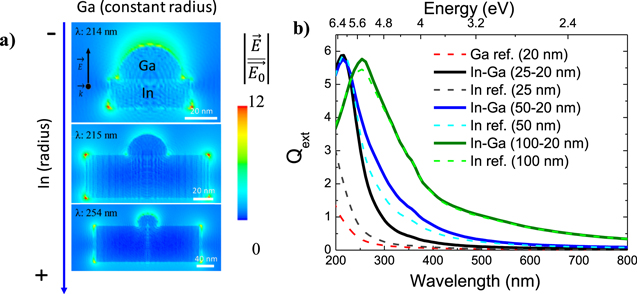
Standard image High-resolution imageFigure 7(a) shows the local electric field distribution when we have changed the In NP size from 25 to 100 nm in radius, while Ga NP is kept constant at 20 nm in radius. The enhancement of the electric field is maximum when the NPs have similar dimensions. This enhancement is evidenced in figure 7(a), where the hot-spots are visible not only around the two NPs system, but also in the interface between Ga and In. Nevertheless, when In NPs increases, the hot-spots appears only at the corners of In NPs. Thus, it suggests that the main contribution in these cases, are due to the In NPs rather than to the coupling effect. Figure 7(b) shows the Qext analysis when Ga NP is on top of In NP. Moreover, we have compared in the figure the Qext of the hybrid system together with Ga and In NPs references. Under this configuration, the results also indicate that the optimal case of the out-of-plane LSPR coupling is when Ga and In NPs have similar dimensions, thus, both plasmon resonances contribute to the coupling. When In is too large in comparison with Ga, there is no overlapping of the hot spots of the particles and then the main contribution to the LSPR is due to the largest particle (i.e. In in our configuration). However, Ga seems to contribute also with small broadening but, remarkably, not to the redshift.
Figure 7. DDA out-of-plane simulations for the hybrid system Ga on top of In. Figure (a) shows the placement of the NPs and the local electric field distribution of the out-of-plane mode when the size of the In NPs increases (from A to B) while Ga NP radius is kept constant at 20 nm. (b) The calculated Qext for single Ga NP as reference (red dashed line) and different NPs sizes: In is similar to Ga (dark line), In reference A (dark dashed-line), In is larger than Ga (blue line), In reference B (light blue dashed-line), In is much larger than Ga (dark green) and In reference C (light green dashed-line).
Download figure:
Standard image High-resolution image
The simulations show a qualitatively good agreement with the experiments considering the limitations of the model, restricted to the two-particle system. The near-field enhancement is optimized when Ga and In NPs have similar dimensions, but the distribution of the NPs (lateral or vertical coupling) affects the intensity of the main hot-spot. According to these results, the broadening and the redshift of the LSPR should be mainly ascribed to the in-plane mode coupling, since the out-of-plane coupling shows a weak effect in the different tested sizes.
4. Conclusion
We have successfully produced hybrid In-Ga systems with a spectrally broad LSPR by adapting the mass (and size) of both NPs. We found that is possible to avoid the eutectic phase thanks to the core-shell structure. The position, width and intensity of the LSPR can be optimized by combining different sizes of the NPs. The hybridization causes a redshift in all the cases and, at the same time, an enhancement in the absorption due to the resonances coupling. The broadening of the LSPR can be as high as 812 nm (or 1.53 eV), being the optimal value found when Ga and In NPs have similar dimensions. DDA simulations confirm this finding and, additionally, show that the broadening is dominated by in-plane coupling, rather than by out-of-plane. This use of plasmon-particles coupling opens the door for further developments to control the light–matter interaction, e.g. in biosensing and solar cell platforms.
Acknowledgments
The authors thank Eduardo Ruiz for technical support during the sample preparation. ARC acknowledges the Ramón y Cajal program (under Contract Number RYC-2015-18047). This research is supported by MINECO (CTQ2017-84309-C2-2-R, CTQ2014-53334-C2-2-R) and Comunidad de Madrid (TRANSNANOAVANSENS P2018/NMT 4349) projects.