

Abstract
The mutual interaction of the type II heterointerface can be very susceptible to the variation of electron states, introducing differences into the band structure and the band alignment in comparison to their pristine states. Here, the thermal evolution of the exciton transition and electronic properties inside the covalently bonded type II interface of the atomically planar WSe2–WS2 lateral heterojunction has been studied. With the aid of luminescence and electronic evolution, it was found that the coupling at the heterointerface is strong, and that the change in the photon–electron transition with temperature is weak. Meanwhile, by employing some quantitative computational methods, the temperature variation of the extracted built-in electric field at the interface is unexpectedly pronounced, resulting from the thermodynamical spanning behaviors of the electrons, as well as the strains generated by the difference in the thermal expansion coefficient between the structural lattice. In addition, the electric contact at the interface shows a negative temperature correlation. The present findings provide a vital contribution to the photo–electron interaction-based application and evaluation paths of the electric contact in two-dimensional transition metal dichalcogenide-based devices.
Export citation and abstract BibTeX RIS
1. Introduction
Possessing several tunable properties, such as carrier density, band gap, band offset, and polarity, two-dimensional (2D) transition metal dichalcogenides (TMDCs) are regarded as promising candidates for applications in photoelectric and energy conversion devices [1–5]. Performance optimization, such as a faster response frequency or lower power dissipation, strongly relies on interfacial states, which are dominated by electronic behaviors, such as photon–electron coupling effects and the electron transfer process across the interface [4, 5]. Previous works have realized the phase transition from semiconductor to metal of MoTe2 thin films, and successfully reduced the Schottky contact barrier at the gold/TMDC interface [6–8]. In addition, a few groups have achieved low contact resistance between metallic graphene and other 2D materials [9]. Nevertheless, their practical applications were hindered by large scale fabrication [9, 10]. Luckily, large area lateral heterojunctions comprised of monolayer 2D TMDCs have been successfully grown recently [1, 2, 11–14]. As the milestone materials are of unique structures with two kinds of 2D TMDC materials covalently bonded at the interface, the in-plane 2D lateral heterojunctions have evoked significant interest in the investigations of photoelectric properties and electric contacts at the interface [1, 12–17]. The interface of the 2D lateral heterojunctions exhibited typical p–n diode behaviors with remarkable electric properties of current rectification and photocurrent generation effects by the current–voltage (I/V) characterizations reported in previous works [1, 12–14, 16, 18–20]. However, the thermal-induced changes of the photon–electron interaction or band alignment properties, as well as the electronic distribution evolution at the heterointerface, have been seldom demonstrated in the 2D planar WSe2–WS2 lateral heterojunction.
In this work, the coupling interaction of the covalently bonded interface and its in situ electronic properties in a monolayer WSe2–WS2 lateral heterojunction have been systematically studied. By variable temperature tuning the electron transition, the band parameters change when the band structure is modulated. The location of the photon–electron interaction can effect the exciton transition energy of the interband, resulting in a blueshift of photo–excitons from a direct to indirect transition. The coupling strength for the covalently bonded interface is strong, which is revealed by the weak changes of photon energy. In addition, an in situ exploration is performed to gain direct insight into the thermodynamic electron evolution at the interface. It is found that temperature is a sensitive factor which specifically adjusts to the carrier distribution as well as the strains generated by the difference in the thermal expansion coefficient between the lattice. Furthermore, with quantitative computational methods, some associated parameters have also been extracted to evaluate the electric contact evolution. These investigations contribute to the estimation of the energy dissipation-induced thermogenesis in photoelectric devices, which can secure the long-term stability of the 2D TMDC-based circuit.
2. Experimental section
2.1. The growth of the WSe2–WS2 lateral heterojunction
The 2D monolayer WSe2–WS2 heterojunction was grown by a two-step epitaxial chemical vapor deposition method on an Si/SiO2 substrate. Two quartz boats with WSe2 and WS2 powder were loaded into a horizontal tube furnace with a quartz tube. A clean Si/SiO2 substrate was placed at the downstream end of the furnace as the growth substrate. The system was pump-purged with argon (Ar) gas and then ramped to the desired growth temperature for the growth of the WS2 nanosheets at 1150 °C for 20 min under ambient pressure and a constant flow of 300 sccm Ar worked as the carrier gas. Then the boat with WS2 powder was pushed out of the hot zone without breaking the vacuum, while the boat with WSe2 powder was simultaneously pushed into the hot zone of the tube in situ. The temperature was then ramped to 1190 °C for the lateral epitaxial growth of the WSe2 for about 20 min under 500 sccm Ar flow. Then the growth was terminated by shutting off the power of the furnace, and the sample was naturally cooled down to ambient temperature.
2.2. Microstructure exploration
The Raman scattering and photolumiscence (PL) measurements were implemented on a confocal microscope system (Jobin-Yvon LabRAM HR Evolution spectrometer) with a 532 nm excited laser. A grating of 1800 grooves mm−1 for Raman and 600 grooves mm−1 grating for PL was used to collect the spectral data. A THMSE 600 heating/cooling stage (Linkam Scientific Instruments) was used in the temperature range from 305 K–405 K with a resolution of 0.1 K. The topography and surface potential images of the sample were simultaneously obtained from the KPFM technique (Bruker, Dimension Icon SPM) in LiftMode, with dual-pass scanning. To avoid oxidation of the sample during the heating process, we performed all of the above in a dry N2 atmosphere. Further, to arrive at the thermal equilibrium state of the charge transferring across the interface of the heterojunction, the temperature ascending speed was controlled at a rate of 5 K min−1 and temperature plateaus of 60 min. The tip bias was adjusted to cancel out the capacitive force by the KPFM system, according to the relation ϕsample = ϕtip − eCPD, where CPD represents the contact potential difference between the tip and sample and e is the elementary charge, respectively. The parameters ϕsample and ϕtip are the workfunctions of the sample and tip, respectively. The workfunction of the Pt/Ir-coated tip (ϕtip) was calibrated to be 4.48 eV using a freshly exfoliated surface of highly oriented pyrolytic graphite (HOPG), of which the workfunction (ϕHOPG) is assumed to be 4.47 eV [21]. The dimension heater/cooler could heat the sample from 300 K to 405 K with an accuracy of 1 K.
3. Results and discussion
3.1. Microstructure verification
Figure 1 shows the spatial distribution structures and optical properties of the planar WSe2–WS2 lateral heterojunction. The optical contrast between the inner and outer triangle shows the core–shell structure of the WSe2–WS2 lateral heterojunction. The AFM image (85 × 85 μm2) in figure 1(b) confirms that the WSe2–WS2 heterojunction is monolayer, with a thickness of approximately 0.8 nm for the shell region and 0.6 nm for the core region, respectively. Figures 1(c)–(e) show the Raman images that map at 257.2 cm−1 corresponding to the  resonant mode of WSe2 and 338.1 cm−1 corresponding to the E12g resonant mode of WS2, respectively. PL intensity maps at 1.69 eV and 1.87 eV are further applied to characterize the distinct core–shell structure. We can clearly see that the PL peak around 1.87 eV is mainly localized at the inner layer (WS2) while 1.69 eV for the outer layer (WSe2). From figures 1(c)–(h), the spatial composition distribution within the WSe2–WS2 heterojunction further verifies that the monolayer WSe2 periphery region is laterally epitaxially connected with the edge of the monolayer WS2 core region.
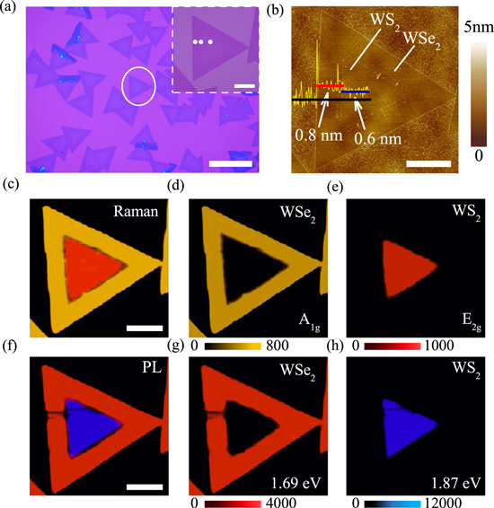
Figure 1. (a) Optical images of the WSe2–WS2 heterostructure. The scale bar is 100 μm. The inset shows the circled zone. (b) AFM image of the monolayer WSe2–WS2 heterostructure. Raman intensity maps at (d) 257.2 cm−1 (A1g resonant mode of WSe2) and (e) 338.1 cm−1 (E12g mode of WS2). PL intensity maps at (g) 1.69 eV of the outer WSe2 and (h) 1.87 eV of the inner WS2. (e), (f) The combined maps. Note that all the scale bars are limited to 20 μm.
Download figure:
Standard image High-resolution image3.2. Band structure evolution
Figure 2(a) shows the PL spectra taken from the point labeled in the inset of figure 1(a). The band structures at different positions in the heterojunction are distinct in the Gaussian fitting. The photon-excited electron–hole pairs will separate and relax to the conduction band edge of WSe2 and the valence band edge of WS2, as shown in the schematic diagram of figure 3(a). The distinct peaks at 1.68 and 1.87 eV correspond to the interband excitation for the pristine WSe2 and WS2 with a direct band gap, respectively. There is a gradual blueshift of the PL exciton position of pristine WSe2 closing to the interface. Considering that the PL intensity of WS2 is stronger than that of WSe2, this behavior in WS2 is negligible. The profile shows that the exciton energy at the interface is approximately 60 meV higher than that of the pristine WSe2 district. However, the emission energy of pristine WS2 is approximately 8 meV higher than that of the interface region. Previous works have demonstrated that photon–electron interactions in semiconductor materials can be seriously affected by chalcogen composition [22–24]. The optical properties of 2D TMDC alloy nanosheets, such as the band gap or the Raman frequency modes, can be varied linearly with stoichiometric compounds of a tunable sulfur ratio [23, 24]. Here, the prominent deviation of the PL emission energy between the pure and interface region in the WSe2–WS2 heterojunction is presumably due to the mixed alloying of the chemical composition around the interface region. In other words, the S atoms are believed to coexist with Se atoms with a gradually changing stoichiometric ratio from pure WSe2 or WS2 to the alloying interface. Moreover, figure S1 (available online at stacks.iop.org/NANO/29/435703/mmedia) depicts the Raman spectra of the sample, which shows the peak positions shifting from pure WSe2 or WS2 to the interface region when the value of the  mode is 3.07 cm−1 for WSe2 and the
  mode is 3.44 cm−1, and the
  mode is 1.99 cm−1 for WS2, respectively. Therefore, the shifting behavior in both the PL and Raman spectra can confirm the hypothesis of the existence of a chemical composition transition region around the interface.
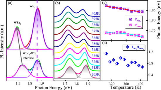
Figure 2. (a) The Gaussian fitting PL spectra of the WSe2, WS2 and the interface areas in the heterostructure domain as marked by the white dots in the inset of figure 1(a). (b) Normalized temperature-dependent PL spectra of the interface at the lateral heterostructure. (c) Peak position of WSe2 and WS2 extracted from the heterointerface. (d) The intensity ratios between WS2 (I1) and WSe2 (I2).
Download figure:
Standard image High-resolution image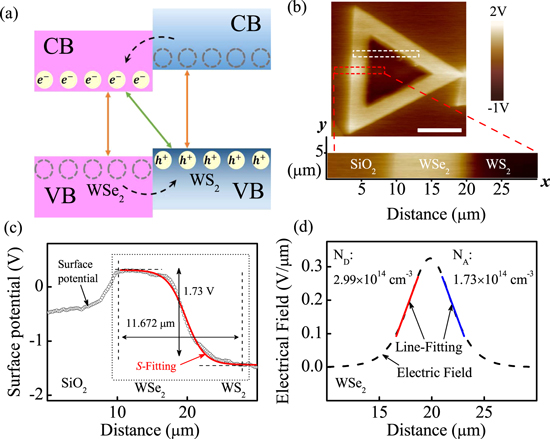
Figure 3. (a) Schematic diagrams of the band alignment of the WS2–WSe2 heterojunction. (b) The top panel is the surface potential image of the WS2–WSe2 heterostructure domain. The bottom panel is the selected area marked by a red dashed rectangular in the top panel for detailed analysis. Note that the scale bar is 20 μm. (c) Surface potential distribution at the WSe2–WS2 interface and its sigmoid function fitting curve. (d) Built-in electric field distribution at the interface of the WS2–WSe2 heterojunction.
Download figure:
Standard image High-resolution imageThe detailed temperature evolution of the electron transition for the covalently bonded interface in the WSe2–WS2 heterojunction is shown in figure 2(b). The photon energy of WSe2 (P ), WS2 (P
 ) is fitted with the integrated intensity peak, on purpose to describe the intensity variation trend with temperature. Figure 2(b) displays the luminescence intensity evolution of the heterointerface as a function of temperature from 305 K–405 K with a stability of about 0.1 K. The PL spectra can be deconvoluted into two major peaks. Along with the variation of the luminescent intensity, the direct transition in the heterostructures experiences a gradual redshift as the temperature increases, as shown in figure 2(c). Such behavior is similar to the response of conventional semiconductors under high temperature, which can be attributed to increased phonon–exciton interactions and slight changes in bonding lengths. Thus, it provides a route to evaluate temperature correlations to the semiconductors. The temperature dependence of the PL peak position is fitted by employing the modified Varshni relationship:

where E0 is the emission energy at zero absolute temperature, S is the Huang–Rhys factor which can reflect the coupling strength between the exciton and phonon,  is the average phonon energy, and ℏ and kB are the Plancks and Boltzmann constant, respectively. The fitting values of E0, S, and
  of WSe2, WS2 are extracted in table 1. By comparing the fitting parameters of the TMDCs at the interface, such as S, the contribution of the interface coupling can be informed. In addition, the temperature difference between WSe2, WS2 at the interface can also be derived by comparing the measured difference between the emission PL energy. The variation with temperature of the peak
  and
and  at the interface do not disply a redshift as obvious as in the pristine WSe2, WS2 monolayer, which is a reflection of the strong coupling interaction between the exciton and phonon at the covalently bonded interface. Furthermore, the intensity ratio (I
 /I
/I ) has been plotted to reflect the competing evolution of the exciton quantities between WSe2 and WS2 in variable temperature processes. The decrease of the intensity ratios, as shown in figure 2(d), also represents the direct–indirect spectral-weight conversion with the increasing temperature.
Table 1. The parameter values of the modified Varshni model for peak energy at the interface as a function of temperature in figure 2(c).
| Sample | Exciton | E0 (eV) | S |
 (meV) (meV) |
|---|---|---|---|---|
| WSe2–WS2 | P
|
1.96 | 3.43 | 8.13 |
| Interface | P
|
1.74 | 2.78 | 6.23 |
3.3. The electron states evolution
Figure 3(a) schematically depicts the type II band structures of the covalently bonded interface. From the surface potential image in figure 3(b), the workfunction of the shell WSe2 is lower than that of the core WS2. The discriminating difference between the Fermi levels of these two materials, which forms the built-in potential barrier, can facilitate the photo-excited electron–hole separation and verify the type II band alignment with an atomically sharp heterointerface. Neglecting the hybridization of electronic states in the WSe2 and WS2 layers, the lowest conduction band resides in WSe2 and the highest valence band resides in WS2, respectively [12, 16, 18, 20, 25]. Likewise, in the WSe2–WS2 heterostructure, due to type-II band alignment, photo-excited electrons and holes will relax (dashed lines in figure 3(a)) to the conduction band edge of WSe2 and the valence band edge of WS2, respectively.
As shown in figure 3(c), the value of the surface potential is averaged along the y-axis direction in the bottom panel of figure 3(b) under the thermal equilibrium condition, from which we can conclude that the WSe2–WS2 heterojunction serves as a quasi planar n–p junction, where the WSe2 works for the n-side and WS2 for the p-side. Treating the surface potential distribution with a sigmoid fitting function (S-fitting) below: [26, 27]

Here, A1 = 0.281 and A2 = −1.433; dx = 1.083 and x0 = 9.242 μm form the frontier between the quasi p-type region and n-type region, respectively. The distinction between the inherent Fermi levels of WSe2 and WS2 (△EF) can be calculated by estimating the CPD difference between the WSe2 and WS2 sides (△CPD :
:
Together with the S-fitting results, we can evaluate the value △EF and the depletion region width to be approximately 1.73 eV and 11.67 μm, respectively. Meanwhile, the potential drop at the WSe2/SiO2 interface can be attributed to the abrupt height change, or the work function differences between semiconductor WSe2 and insulator SiO2 [28].
Furthermore, by differentiating the sigmoid fitting profile, we obtain the built-in electric field distribution, as shown in figure 3(d). The formed built-in electric field locates at the interface zone that impedes the dynamic diffusion of carriers. We use the below equations to define the built-in electric field distribution (ξ(x)) of the 2D abrupt junction: [29, 30]


It is noteworthy that 
 = 6.1 and
  = 11.7 are the dielectric constant of monolayer WS2 and WSe2 [16, 19], respectively. The parameter 0 is the vacuum permittivity. ρ
 and ρ
and ρ are the screening lengths, given by ρ
 = 2πχ
= 2πχ and ρ
and ρ = 2πχ
= 2πχ , where χ
 = 0.718 nm and χ
 = 0.603 nm are polarizabilities of monolayer WSe2 and WS2, respectively [31]. The maximum electric field is estimated to be 32.52 V cm−1, almost locating at the midpoint of the depletion region. Moreover, the amount of the intrinsic doping concentration is derived from the slope of the linear fitting of the electric field distribution. It can be concluded that nD ≈ 2.4 × 107 cm−2 in n-type WSe2 and nA ≈ 1.04 × 107 cm−2 in p-type WS2, respectively. This result is reasonable when compared with the intrinsic carrier concentrations (∼1010 cm−2) reported in previous work [1, 16, 19]. Among which, Wn and Wp are the depletion width in WSe2 and WS2, respectively. The total depletion width W = Wn + Wp, which is the varying part of the surface potential profile along the x-axis direction, can be obtained by the p–n junction modeling below: [19, 32]


According to the relations ND[A] = nD[nA]/tn[p], t is the thickness of the monolayer in-plane heterojunction and can be read directly from the AFM image (t ≈ 0.8 nm, t
 ≈ 0.6 nm). So ND ≈ 2.99 × 1014 cm−3, NA ≈ 1.73 × 1014 cm−3. In addition, the modeling predicts the depletion width Wn and Wp to be approximately 1.43 and 2.48 μm respectively, compared with the estimated value (W ∼ 11.67 μm). This implies that the theoretical p–n heterojunction modeling, which is based on the assumption of no free carriers and constant dopant concentration for the intentionally doped inorganic semiconductors with high-carrier mobility [32], is not completely suitable for describing electronic transport in the 2D covalently bonded heterojunction, and remains to be explored.
Considering the heating phenomenon in the practical integrated circuit of the photoelectric devices, we performed temperature-dependent (305 K–405 K) characterization utilizing the KPFM technique, which was conducted in a N2 atmosphere. Figure 4(a) displays the surface potential mappings of the WSe2–WS2–WSe2 interface at different temperatures. It distinctly shows that the surface potential of WSe2 declines with temperature, and the WS2 manifests an opposing tendency. The variation of the surface potential reflects the thermodynamic charges transferring across the WSe2–WS2–WSe2 interface. An n–p to p–n junction transition emerges at the critical point of temperature (Tc, 365 ∼ Tc ∼ 375 K) [33]. For clarity, we plotted the horizontal profiles of the surface potential distribution at the WSe2–WS2–WSe2 interface, as shown in figure 4(b). It is noteworthy that each of the curves is averaged along the y-axis direction in figure 4(a) at the corresponding temperature. A flat band condition is reached at Tc, where the value of the workfunctions from the WSe2 and WS2 sides stay very close, implying that a zero-barrier ohmic contact between WSe2 and the WS2 side is formed.
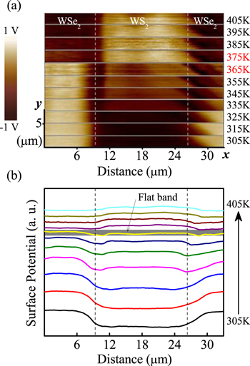
Figure 4. (a) Surface potential images at the WSe2–WS2–WSe2 interface for variable temperature ranging from 305 K–415 K with a step of 10 K. Note that the mapping region is located in the white dashed rectangle marked in figure 2(b). (b) Surface potential distribution at the WSe2–WS2–WSe2 interface within variable temperature.
Download figure:
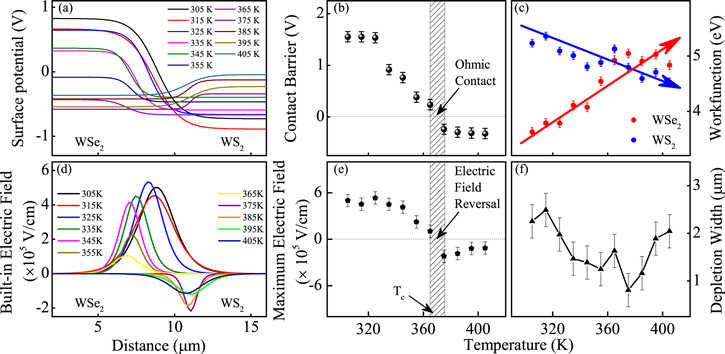
Standard image High-resolution imageTo understand the intrinsic mechanism of the electronic states during the period of the temperature increase, the surface potential profiles of the WSe2–WS2 interface in the whole temperature range are plotted in figure 5(a). Each curve is fitted by the sigmoid function as discussed above. The closed Fermi levels of WSe2 and WS2 at Tc benefit the thermodynamic behaviors of the carriers traveling through the WSe2–WS2 interface. For a detailed view of the dynamic variation of the electric contact between WSe2 and WS2, the built-in potential barrier with temperature is derived in figure 5(b). Obviously, the positive value of the contact barrier tends to decline with an increase in temperature, indicating a negative temperature correlation of the built-in contact barrier. This shows a decrease in the contact resistance with an increase in the temperature of semiconductor devices, unlike the resistance in the semimetal devices of the 1T' phase [34]. The mostly weakened barrier (∼0 V) emerges, implying that the electric contact is effectively tailored at Tc. When the temperature is beyond Tc, the contact barrier between the WSe2 and WS2 side increases with a negative value. Consequently, the charge injection from WSe2 to WS2 is hindered, rendering a relatively opposing diffusion from WS2 to WSe2.
Figure 5. (a) S-fitting curves of the surface potential at the WSe2–WS2 interface at different temperatures. (b) Built-in contact barrier variation and (c) workfunction variations of WSe2 and WS2 at different temperatures, respectively. (d) Built-in electric field distribution at different temperatures. (e) Maximum electric field and (f) depletion width plots at different temperatures, respectively. Note that the width of the shadow rectangles in panels (b) and (e) represent the critical temperature.
Download figure:
Standard image High-resolution image
Since the specific resistivity inside the semiconductors can be strongly affected by the doping level, we have explored the variation of the intrinsic carrier concentration, which is indirectly displayed by the workfunction profile. As shown in figure 5(c), the workfunction variation of WSe2 and WS2 with temperature is deduced. Note that the Fermi levels shift in the opposite direction with the workfunction; the profile shows that both the amount of carriers in the n-type WSe2 and p-type WS2 sides decrease with temperature. This phenomenon is inconsistent with the view that the higher the temperature, the greater the chance of the carriers being thermally excited. Bearing in mind that the environment, such as substrate and ambient, has a strong impact on the doping concentration of carriers [35], it can be concluded that the drop in the amount of carriers can thus be attributed to the electron-withdrawing effect induced by the Si/SiO2 substrate of the WSe2–WS2 heterojunction. [9, 36].
Considering that the electric field poling is sensitive to temperature [37], the spatial distribution of the built-in electric field at different temperatures is obtained by differentiating the work function, as shown in figure 5(d). The pronounced transformation of the built-in electric field can be due to the thermal transferring behaviors that result in the change of electron location at the lattice, which is very susceptible to structural strain along the lattice distribution at the interface. The direction of the built-in electric field gradually reverses at Tc. This evolution of the built-in electric field with the increasing temperature process is assumed to be the difference in the thermal expansion coefficient (TEC) between the WSe2 and WS2 materials, which can induce a structural mismatch of the lattice [33]. Previous work has reported that the TEC mismatch would induce a strain effect in the 2D materials [38]. To verify the strain effect during the temperature varying process, the temperature-dependent Raman spectroscopy at the interface of the WSe2–WS2 lateral heterojunction is utilized, as shown in figure S2(a). The peak position behaves as a function of temperature for the frequency modes of WS2 and WSe2, as shown in figure S2(b)–(d), which we conclude to be the contribution from the thermal anharmonic effect and the thermal expansion [38–41]. In addition, there is a discrepancy in the extracted slope of the linear fitting from the Raman modes versus temperature, which is consistent with previous work [42]. These results accordingly confirm that the strain effect is a consequence of the difference between the thermal coefficient of these materials.
Based on equations (5) and (6), the depletion width at variable temperature is deduced in figure 5(f). The width shrinks till it reaches the minimum value at Tc. When the temperature is beyond the Tc, the width of the depletion region gradually increases, which indicates that the unit cells recover their cubic shape. We concluded that this is due to the thermal diffusion of the intrinsically excited carriers. Due to the fact that the generated holes and electrons move towards the opposite direction and approach the border of the depletion region, the depletion width declines.
4. Conclusion
In summary, the in situ thermal exploration of the photon–electron and electronic evolution of the type II interface in a monolayer WSe2–WS2 lateral heterojunction was performed. The exciton transition energy relating to the photon–electron interaction experienced a blueshift from pristine materials to the interface, which was attributed to the direct-to-indirect exciton transition of the interband. The coupling strength for the covalently bonded interface was strong which was revealed by the weak shift of the photon energy with temperature. Nevertheless, the evolution of the lattice strain effect was magnified by the obvious variation of the built-in electric field with temperature through the computational methods for extracting the electron distribution. In addition, the electric contact at the interface has shown a negative correlation with temperature that facilitated more carrier spanning behaviors. Our results emphasize the evolution relation between the light emission and electronic states of the type II interface in lateral heterojunctions, and they contribute to providing universal paths to the evaluation of the electrical contact for fundamental investigation as well as TMDC-based photodioxide devices.
Acknowledgments
This work was financially supported by the National Key R&D Program of China (Grant Nos. 2018YFB0406500 and 2017YFA0303403), the National Natural Science Foundation of China (Grant Nos. 61674057 and 61227902), the Projects of Science and Technology Commission of Shanghai Municipality (Grant Nos. 18JC1412400, 18YF1407200, 18YF1407000, and 15JC1401600), and the Program for Professor of Special Appointment (Eastern Scholar) at Shanghai Institutions of Higher Learning and the Fundamental Research Funds for the Central Universities.