

Abstract
Suppression of magnetoresistance (MR) is meaningful for sensor applications to immure magnetic fields. Herein, we report the observation of suppressed MR in PtSe2 microflakes by introducing the antidot arrays (AAs). We have compared the magnetotransport properties of PtSe2 microflakes before and after milling of AAs. The enhanced resistivity and notable MR suppression were observed while the AAs are milled in the PtSe2 microflakes. Their physical mechanism has been ascribed to the enhanced electron scattering rate due to the additional electron–antidot interactions. This work gave an example to suppress MR in materials by introducing AAs, which may be useful for sensor applications in magnetic fields.
Export citation and abstract BibTeX RIS
Platinum diselenide (PtSe2) is a recently discovered two-dimensional (2D) transition metal dichalcogenide [1, 2], its exotic spin texture gives an application opportunity in electrically tunable spintronics [3]. The high electron mobility and air-stability of few-layer PtSe2 devices have aroused great research interest for nanoscale electronic applications [4, 5], such as gas sensing [6, 7] and catalytics [8]. Moreover, the bulk PtSe2 is theoretically predicted as a candidate of the type-II Dirac semimetal [9]. The anisotropic three-dimensional Dirac cones with the Dirac cone highly tilted along the kz direction in the Brillouin zone are experimentally observed by using angle-resolved photoemission spectroscopy [10]. Therefore, the electrical transport study of PtSe2 devices is very important not only for fundamental physics, but also for future applications in electronics and catalysis.
Magnetoresistance (MR) is a key property to examine the electron transport mechanisms in materials and devices, and is also applied in variety areas, such as magnetic field sensing and magnetic storage [11–13]. For a nonmagnetic material, its MR has the attractive features such as no magnetic hysteresis and high MR value, making it has potential application in magnetoelectronics devices [14–16]. However, in some cases, for example, to measure the temperature, or gas concentration, or humidity in a magnetic field environment, the MR of sensitive materials will lead to a measurement error [17–19]. The high MR value and the large measurement error. Therefore, the suppression of MR is useful for the sensor applications in the magnetic field environments.
In this work, we report on the suppression of MR in PtSe2 microflakes by introducing the antidot arrays (AAs). AA is a fascinating artificial microstructure, which is consists of an array of holes in a film. The anomalous quantum transport properties of AAs, fabricated on the semiconductor heterostructures, graphene, topological insulators, etc, have been widely investigated previously [20–27]. Here, the AAs were fabricated on the PtSe2 microflakes. We compared the magnetotransport behaviors of PtSe2 microflakes before and after milling of AAs. The notable suppression of MR was observed while the AAs are milled in the PtSe2 microflakes. Our work gave an evidence of MR suppression by introducing AAs in the materials/devices, which may be useful for the PtSe2-based sensor applications to immure magnetic field.
The high-quality PtSe2 bulk crystals were purchased from the commercial company (HQ Graphene, the Netherlands). By using a mechanical exfoliated method, the thin PtSe2 microflakes were transferred onto the silicon substrate covered by 300 nm silica. The Ti/Au (10 nm/150 nm) electrodes were patterned onto the microflakes by a series of processes including the photolithography, electron beam evaporation deposition and lift-off technology. The thickness of the samples was determined by atomic force microscopy. The AA patterns were etched in the PtSe2 microflakes via focused ion beam (FIB) direct writing technology. The electrical transport properties of the PtSe2 devices were measured in a quantum design physical property measurement system.
Figure 1(a) shows a PtSe2 device which prepared the six-probe Hall-type electrodes (denoted as S1). The thickness of S1 is around t = 98 nm. Its length (L, the distance between the two voltage probes) and width (W) are both 10 μm. A periodic distributed AA pattern was etched in this PtSe2 microflakes (figure 1(b)). The average diameter of the antidots was around d = 0.9 μm. As we know, the lattice damages could be occurred by the Ga ion implantation of FIB technology. The serious damages could alter the crystal structure of PtSe2 materials. To overcome this disadvantage, we kept the ratio d/a = 0.5 (a is the center-to-center distance between the adjacent antidots) in our experiments. In such case, the PtSe2 materials can not be completely damaged after AA fabrication [28]. Figure 1(c) shows the Raman spectrums of the PtSe2 device before and after AA milling. The Raman peaks at 175 and 205 cm−1 are belong to the Eg and A1g modes of PtSe2 crystal. The notable Raman modes are both observed in PtSe2 device with and without AAs, this result demonstrated that the PtSe2 crystal structure is not changed after FIB machining.

Figure 1. General characterizations of a PtSe2 device (sample S1). (a) The optical image of the device before antidot milling. (b) The scanning electron microscopy (SEM) image of the PtSe2 device after antidot milling. (c) The Raman spectrums of the PtSe2 flakes with and without antidot arrays (AAs). (d) The temperature dependence of resistance of the PtSe2 device with and without AAs. (e) The Hall resistance as a function of magnetic field B of the PtSe2 device with and without AAs at T = 2 K. The inset shows the Hall resistance curves at T = 300 K for the PtSe2 device. (f) The cartoon picture illustrating the two electron diffusion paths, the path ② presents the additional electron–antidot scattering.
Download figure:
Standard image High-resolution imageFigure 1(d) displays the temperature dependence of resistance of sample S1 with and without AAs. We can see that, after etching AAs, the device's resistance increased compared with the pristine microflake. For sample S1 at T = 2 K, we could obtain that 
 and
and  Furthermore, we could obtain the bulk resistivity
  for the pristine sample. While the AAs were etched in the PtSe2 microflake, the effective volume of materials
  can be estimated by
  where N is the total number of antidots. Then, we could obtain the bulk resistivity of flakes with AAs
  and
and  If we suppose that any resistance increase in PtSe2 microflakes would result from a reduction of the flake's cross-sectional area for the current path, then we should observe that
  Obviously, this assumption is conflict to the experimental results, the detailed reasons should be further investigated.
Hall resistance of PtSe2 microflakes was also measured. Figure 1(e) presents the  curves of sample S1 with and without AAs at T = 2 K. Then, we could extract the electron concentration
  and
and  for S1 without and with AAs respectively. By repeating the above sequence, we could obtain the relevant parameters for S1 at T = 300 K, and the results have been listed in table 1. We can see that
  in the studied temperature range. We expect that the electron effective mass
  is nearly unchanged in PtSe2 microflakes while introducing AAs, that is,
  According to
  where e is the electron charge and τ is the elastic scattering time, we found that
  Therefore, the significant increase of the bulk resistivity is originated from the enhanced electron scattering rate (1/τ) introduced by the AAs. As shown in figure 1(f), there are displayed two types of electron diffusion paths in the nanostructured flakes. The path ① presents the carriers transport in the bulk materials without the electron–antidot interactions (corresponding scattering time denoted as τ1). If the electron–antidot scattering time τea is take into account (the path ②), the total electron scattering rate can be expressed as
  Obviously, the electron scattering rate is enhanced while appearing AAs in PtSe2 flakes.
Table 1. Parameters of sample S1.
| R (Ω) | ρ (μΩ m) | n (1021 cm−3) | |||||||
|---|---|---|---|---|---|---|---|---|---|
| T (K) | w/o AA | AA |

|
w/o AA | AA |

|
w/o AA | AA |

|
| 2 | 0.54 | 44.76 | 83 | 0.053 | 1.597 | 30 | ∼0.96 | 1.54 | ∼1.6 |
| 300 | 3.53 | 91.72 | 26 | 0.346 | 3.272 | 9.5 | 7.78 | 8.73 | 1.1 |
Figure 2 displays the MR curves of sample S1 with and without AAs. We can see that the MR values of PtSe2 microflakes with AAs are greatly suppressed comparing to that of the pristine PtSe2 microflakes (figures 2(a), (b)). For example, MR = 121% and 8% for S1 without and with AAs respectively, at T = 2 K, where MR = [R(B) − R(0)]/R(0) × 100%. If we define  we could obtain
  for S1 at T = 2 K. With the temperature increasing, the MR is weakened both PtSe2 microflakes with and without AAs (figures 2(c), (d)). Nevertheless, the MR of AA device is always suppressed in the studied temperature range compared to the pristine device. The suppressing factor
  is decreased with temperature increasing. The insets of figures 2(c), (d) show the Kohler plot of the MR data of S1 with and without AAs. The MR curves gradually deviated from the universal curve with the temperature increasing, which suggests that the multiple electron scattering processes are dominate in the PtSe2 microflakes with and without AAs.
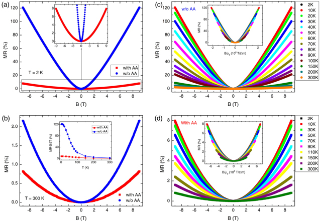
Figure 2. Magnetoresistance (MR) of the PtSe2 device (sample S1). (a) The MR curves of the PtSe2 device with and without AAs at T = 2 K, the inset is the magnified view of the MR curves. The MR value is defined as ![${\rm{M}}{\rm{R}}(B)=[R(B)-R(B=0)]/R(B=0)\times 100{\rm{ \% }}.$](https://content.cld.iop.org/journals/0957-4484/29/40/40LT01/revision2/nanoaad349ieqn25.gif) (b) The MR curves of the PtSe2 device with and without AAs at T = 300 K. The inset shows the temperature dependence of MR values at B = 9 T for PtSe2 device with and without AAs. (c) and (d) show the MR curves at various temperatures for the PtSe2 device without and with AAs, respectively. The insets in (c) and (d) show the MR plotted as a function of B/ρ0 for the PtSe2 device without and with AAs, respectively, where ρ0 is the zero-field resistivity.
(b) The MR curves of the PtSe2 device with and without AAs at T = 300 K. The inset shows the temperature dependence of MR values at B = 9 T for PtSe2 device with and without AAs. (c) and (d) show the MR curves at various temperatures for the PtSe2 device without and with AAs, respectively. The insets in (c) and (d) show the MR plotted as a function of B/ρ0 for the PtSe2 device without and with AAs, respectively, where ρ0 is the zero-field resistivity.
Download figure:
Standard image High-resolution imageAs we know, the commensurability effect of MR is usually observed in a strong spatially modulated potential [20, 22, 29], which is associated with the commensurate orbits encircling a specific number of antidots. Obviously, the high carrier mobility of materials is necessary to observe the commensurability oscillations. Furthermore, the resistance peak position, corresponding orbits around 1 antidot, can be estimated as  for our PtSe2 microflakes, where
  is the Planck constant and ns is the 2D carrier density. We can see that B1 is outside of the magnetic field range in this work. And taking into account the low mobility of our PtSe2 microflakes (μ ∼ 0.1 m2 V−1 s−1), the commensurability transport is therefore absent.
Figure 3 shows the transport properties of other PtSe2 devices, the suppressed MR by introducing AAs is further confirmed. Here, three types of AA are prepared in the PtSe2 microflakes. The first type is the periodic distributed AA (sample S2, figure 3(a)). The second type is the quasi-random distributed AA (sample S3, figure 3(d)), in which the every antidot is randomly distributed in the every sub-area while the entire area is periodically divided into N × M sub-areas. The third type is the random distributed AA (sample S4, figure 3(g)), where the antidots are randomly distributed in the entire area. By analyzing the experimental results of S2–S4, the main theses discussed above are confirmed, that is, comparing to the pristine samples, (i) the electron scattering rate is enhanced while introducing AAs, which leads to the increment of resistance for samples with AAs; (ii) the MR is suppressed for all samples while introducing AAs. One interesting phenomenon is that the resistance upturns with decreasing temperatures at T < 50 K for S3 with AAs (figure 3(e)). Moreover, a weakly MR dip around zero-field can be identified for the nanostructured sample S3 (the inset of figure 3(f)). These results may be originated from the weak antilocalization effect due to the quantum confinement effect [28].
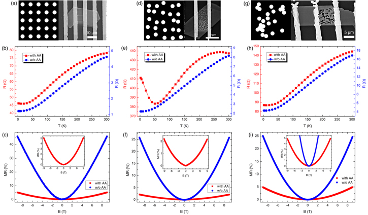
Figure 3. The transport properties of other PtSe2 devices with and without AAs. The left figures in (a), (d), (g) show the periodic, quasi-random and random AA patterns, respectively. The right figures are the SEM images of the PtSe2 devices by milling the periodic, quasi-random and random AAs (denoted as S2–S4 respectively). (b), (e), (h) The R–T curves of sample S2, S3 and S4 with and without AAs, respectively. (c), (f), (i) The MR curves of sample S2–S4 with and without AAs, respectively. The insets in (c), (f), (i) are the magnified views of the MR curves of devices S2–S4 with AAs, respectively.
Download figure:
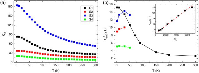
Standard image High-resolution imageIn figure 4(a), we have given a summary of resistance ratio  as a function of temperature for S1–S4. We can clearly see that
  is gradually decreased with increasing temperature. According to above discussions, we have known that the resistance increments of PtSe2 microflakes with AAs are resulted from the scattering rate (1/τea) enhancement of electron–antidot scattering. If we denoted the resistivity of pristine PtSe2 microflakes as
  where τ1 is the electron scattering time including electron–impurity, electron–electron, electron–phonon interactions, and so on. Then, the resistivity of PtSe2 microflakes with AAs can be written as
  Finally, we obtained that

Obviously,  is increases with increasing temperature and
  is nearly independent to the temperature. Therefore, we observed that
  is decreases with increasing temperature.
Figure 4. The transport parameters of the PtSe2 devices with and without AAs. (a) The resistance ratio CR as a function of temperature, where  (b) The magentoresistance ratio
  at B = 9 T as a function of temperature, where
  The legend in (b) is the same as that in (a). The inset in (b) shows the
  as a function of
  for S1.
Download figure:
Standard image High-resolution image
Figure 4(b) plotted the MR ratio  as a function of temperature for S1–S4. At the beginning, we tried to understand the physical mechanisms behind the suppressed MR with AAs. The classical orbital MR theory [30] gives that
  where
where  is the electron mobility. After a few steps simple calculations, we could obtain that

That is,  As shown in figure 4(b) for T = 2 K, we can see that
  is increases with increasing
  for S1, S2 and S4, but S3 is outside with this rule. This may be originated from the quantum interference (weak antilocalization) effect in S3. Let us concentrate on the data at T = 30 K, where the quantum interference effect is weakened in S3, we can see that the scaling law of
  is nearly satisfied. Furthermore, please see the inset of figure 4(b), where
  has been plotted as a function of
  for sample S1. The linear relationship between
  and
and  demonstrates the accuracy of equation (2). Next, according to
  the
the  behaviors can be interpreted by the
  data. That is,
  is decreases with increasing temperature. Finally, we could notice that
  is increases with increasing temperature for
  in samples S2–S4. Obviously, this contradicts with the predictions of
  In our previous work [31], we have reported the anomalous magnetotransport properties of PtSe2 microflakes, that is, the MR value increases with increasing temperature at low-temperature regime. We could expect that the low-temperature
  is dominated by
  due to the
  is suppressed by AAs. We therefore observed the anomalous behaviors of
  at low-temperature regime.
In conclusion, we reported the magnetotransport properties of PtSe2 microflakes with and without AAs. Comparing with the pristine PtSe2 devices (without AAs), the enhanced resistivity and suppressed MR are observed in the PtSe2 microflakes with AAs. The physical mechanism behind above phenomena has been ascribed to the enhanced electron scattering rate due to the electron–antidot interactions. This method by introducing AAs to suppress MR may be useful for PtSe2-based device applications to immure magnetic field.
This work is financially supported by the National Natural Science Foundation of China (Grant Nos. 11604310, 61301015), the National Key Scientific Instrument and Equipment Development Project of China (Grant No. 2014YQ090709), the Key Laboratory of Ultra-Precision Machining Technology Foundation of CAEP (Grant No. ZZ15003) and Hubei Key Laboratory of Pollutant Analysis and Reuse Technique (Hubei Normal University) (Grant No. PA20170204).