

Abstract
As part of the oxygen family, chalcogen (Se, Te) nanostructures have been considered important elements for various practical fields and further exploited to constitute metal chalcogenides for each targeted application. Here, we report a controlled synthesis of well-defined one-dimensional chalcogen nanostructures such as nanowries, nanorods, and nanotubes by controlling reduction reaction rate to fine-tune the dimension and composition of the products. Tunable optical properties (localized surface plasmon resonances) of these chalcogen nanostructures are observed depending on their morphological, dimensional, and compositional variation.
Export citation and abstract BibTeX RIS
As important inorganic materials, the chalcogen family (Se, Te, etc.) have attracted great attention due to their broad applications in optoelectronics, gas sensing, biology, medicine and energy harvesting piezoelectrics, etc [1–6]. The properties and its derived functional nano-devices are highly dependent on the morphologies of chalcogen nanostructures, thus, precise control over geometric dimensions is essential for tuning of various properties including optical, thermal, and electrical characteristics.
In the same group of 6A, elemental Te and Se atoms are covalently bonded in each helical chain along the c-axis with a stacking sequence of ABCABC... and these interchains are bound together via second interaction along the lateral direction in a hexagonal lattice (figure S1 is available online at stacks.iop.org/NANO/29/345603/mmedia). On the basis of the anisotropic crystal structure, elemental Te and Se tend to inherently grow along the c-axis, leading to the formation of 1D morphology [7, 8]. Although many researchers have experimentally synthesized various 1D chalcogen nanostructures through a variety of synthetic methods [8–16], simple and rational solution-based approach for generating 1D chalcogen nanostructures with precisely controlled morphologies remains a great challenge.
Localized surface plasmon resonance (LSPR) is the collective oscillations of free carriers through the interaction between the incident light and nanoparticles with much smaller size than the incident wavelength [17]. In the past few years, various nanostructures such as metals, doped semiconductors, and metal oxides have been intensively studied and demonstrated as practical applications for sensing, enhanced spectroscopies, or photothermal therapy [18–22]. The LSPR could be tunable by varying the size, shape, carrier concentration, and hybridization [23, 24]. A possible surface plasmon resonance from tellurium was reported in the nano-sized regime [25]. However, no report has been provided to demonstrate the systematic study on the LSPR band occurrence when it scales down to nanometer according to the dimensional change. To better understand the LSPR of chalcogen nanostructure, the control over the uniformity regarding the size, shape and composition should be primarily considered. Herein, we report tunable optical properties depending on the morphology, dimension and composition by synthesizing chalcogen (Te, SexTe1−x) nanostructures via rational solution process.
Figure 1 shows as-synthesized Te nanostructures including nanowires (NWs), nanorods (NRs), and nanotubes (NTs) with well-defined morphologies in solution process. The details of experimental procedure are provided in supporting information. The morphology can be modulated based on the nucleation and growth event and thus, the control over reaction parameters such as precursor, surfactant, temperature, pH, and reductant could result in different shapes in final products [26]. For the formation of NWs, Te(OH)6 is reduced by relatively weak reducing agent of hydroxylamine in the presence of PVP surfactant. At the very initial state, tellurium oxides were formed at ∼50 °C. With the increase in reaction temperature, Te oxides became t-Te seeds and were subsequently transformed into Te NWs in 24 h (figure S2). The slow reduction rate is attributed to the weak reducing ability of reductant (NH2OH) with a combination of relatively low temperature (∼98 °C). As-prepared NWs were flexible, very thin (∼8 nm, diameter) and ultralong (several micometers) (figure 1(A)). For the growth of Te NRs, we chose the Na2TeO3 as a precursor since lower valence state of Te+4 of Na2TeO3 than Te6+ of Te(OH)6 can induce fast reduction of Te precursor. Two kinds of Te NRs have been prepared by controlling reaction kinetics. Te NRs with an average diameter of 45 nm and length of 340 nm were synthesized by reduction of Na2TeO3 using ascorbic acid as a reducing agent in EG solvent at 100 °C (figure 1(B)). The reaction was completed in 2 h owing to the fast reduction reaction. To generate and obtain relatively thin and long Te NRs, NaOH was added into reaction mixture as a pH controller. It is well known that the growth of Te nanostructures is very sensitive to the pH value, in which alkaline condition retards the reduction rate of  [27]. As a result, NRs with a smaller diameter (15 nm) and longer length (410 nm) were prepared in 3 h due to the relative slow reduction kinetics in the presence of NaOH (figure 1(C)). Interestingly, Te NTs were generated through the same experimental procedure with that of Te NRs (45 nm thick, 340 nm long) except using half amount of PVP and ascorbic acid as a surfactant and reducing agent, respectively. The growth mechanism could be explained by the combination of two aspects: (I) slow reduction kinetics by decreasing amount of ascorbic acid could cause decrease in Te supersaturation, leading to decrease in the diffusion ability of Te atoms. It promotes tubular morphology via concentration depletion at the surfaces. (II) Insufficient coverage of {101} or {102} planes with PVP could result in stacking or aligning these planes on the initial ones during growth, which is well consistent of results reported recently by Professor Sung's group [28]. As-synthesized Te NTs were several micometers in length and 80–100 nm in outer diameter with thickness of ∼20 nm (figure 1(D)).

Figure 1. Morphology control of Te nanostructures: (A) SEM image of nanowires and (B) nanorods (short, thick). (C) Typical TEM image of nanorods (long, thin). (D) SEM image of nanotubes with an inset of a TEM image showing an edge of single nanotube. (E) UV-visible absorption spectra and (F) its change in LSPR peak of corresponding Te nanostructures.
Download figure:
Standard image High-resolution imageWe found that the color of suspensions was different depending on the morphology of as-synthesized Te nanostructures, which were deep blue (NWs, thin NRs) and gray (thick NRs, NTs) (figure S3). The color difference suggested that the optical properties would be largely different when it comes to its dimension and morphology. The corresponding UV-visible absorption spectra shown in figure 1(E) clearly show the red-shift tendency of absorption peak as the diameter increases from NWs to NTs. Bulk Te has shown only one broad absorption maximum around 300 nm (4.13 eV) while nanocrystalline Te has two absorption band in the range of 0–3 eV and 3–6 eV, respectively [29]. The latter is due to the allowed direct transition from the valence band (p-bonding triplet, VB2) to conduction band (p-antibonding triplet, CB1). The former is assigned to a forbidden direction transition for p-lone pair valence band (VB3) to p-antibonding conduction band (CB1), which falls on the band gap energy in the electronic band structure of Te [29–31]. The energy gap expands as the size of Te decreases down to ∼1.33 eV (Eg,bulk ≈ 0.35 eV) when it exists as Te monolayer [32]. Therefore, the band gap energy is not able to exceed this upper limit value by decreasing dimension of Te nanostructure. In addition, polycrystalline Te is known to have high carrier concentration as much as 1019–20 cm−3 in the range of 300–450 K, which is enough carrier density to develop LSPR [33, 34]. Considering the band gap energy, carrier concentration, and nano-sized regime, the strong absorption peak ranging from 380 to 800 nm of tellurium NW can be originated from plasmon resonance rather than band transition since the absorption is appeared only in the Te nanostructures, not bulk tellurium.
As in metal nanocrystals, LSPR is also observed in semiconductors and metal oxides depending on the carrier concentration and anisotropic shape [17, 34–37]. Moreover, LSPR in the NIR region was reported to be blue-shifted up to visible range by increasing carrier density through a proper doping in metal oxides [36]. In addition to the carrier concentration, the dimension and anisotropic shape can also alter the LSPR behavior. Anisotropic morphology separates LSPR modes for each axis as frequently observed in noble metal nanocrystals. For example, LSPR frequency of Au NRs is split into longitudinal and transverse modes [38]. Unfortunately, in this study, we have obtained only one band centered at 400–800 nm, which can be assigned to transverse LSPR of 1D Te nanostructures. It is continuously red shifted as the diameter of Te nanostructure is increased (figure 1(F)). In semiconductor NRs with high aspect ratio, carriers can be significantly localized, preventing their mobility along the long axis, which can interrupt the occurrence of longitudinal LSPR mode [35]. In addition, the dimension of nanocrystals should be much smaller than the wavelength of incident light for generating LSPR. In this context, longitudinal LSPR of Te nanostructures may not be evolved because of the high aspect ratio and length more than several hundred nanometers along the growth direction (c-axis).
To further investigate the variation of LSPR depending on the dimension and aspect ratio, time dependent shape evolution was observed through TEM and UV–vis absorption spectroscopy during the growth of Te NRs (shown in figure 1(C)) as an example case (figure 2). As the reaction proceeded, nanoparticles formed at very initial state (3 min) grew into NRs in 3 h. The color of suspension gradually changed from light yellow to deep blue (figure 2(A)). The length extended continuously to 21 nm, 30 nm, 49 nm, 72 nm, 160 nm, 265 nm and 406 nm with an average diameter of 7 nm, 8 nm, 10 nm, 11 nm, 13 nm, 14 nm and 15 nm when the reaction time was 3 min, 5 min, 7 min, 10 min, 30 min, 60 min and 180 min, respectively (table S1, figures 2(B)–(G)). Figure 2(H) clearly displays the anisotropic growth profiles that Te NRs predominantly extend along the longitudinal direction, while the diameter variations show a little difference, due to the higher surface energy of growth tips than that of radial surfaces. The aspect ratio was continuously changed from 3 to 27. Note that the reaction was completed in 3 h. Figures S4(A) and (B) show the typical TEM and HR-TEM images of as-synthesized Te NRs in 3 h. The lattice fringes with a spacing about 0.59 nm correspond to the (001) plane of hexagonal Te crystal structure. All peaks in the x-ray diffractogram are well indexed to the hexagonal phase of tellurium (JCPDS 36-1452) (figure S4(C)). The corresponding series of UV–vis absorption spectra obviously show that LSPR peaks are red shifted from 380 to 680 nm depending on the diameter of NRs (figures 2(I), S5).

Figure 2. (A) A photograph of Te colloidal suspensions taken out at different reaction time during the growth of Te nanorods. (B)–(G) TEM images showing the temporal change of Te seeds to nanorods. (H) The variation of length and diameter and (I) UV-visible absorption spectra of Te nanorods at different reaction durations.
Download figure:
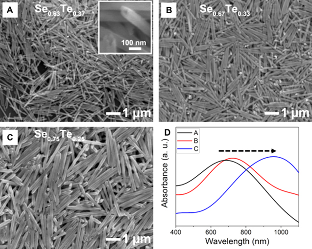
Standard image High-resolution imageTo tune its optical property through making an alloy nanostructure, we have synthesized SexTe1−x NTs with different compositions via varying the molar ratio between Se and Te precursors ([H2SeO3]:[Te(OH)6] = 1.7:1, 2:1, 3:1) (figure 3). Elemental Se and Te have identical crystal structures with the same valence electronic structure, as well as small differences in atomic size and electronegativity. According to the Hume-Rothery rule [39], Se and Te atoms can be randomly located in its trigonal crystalline structure in a manner of binary solid solution (SexTe1−x). The atomic composition of as-synthesized SexTe1−x alloy NTs were well matched with its initial molar ratio (figure S6). When the atomic ratio of Se was enhanced, the average outer diameter and length were increased as 90, 130, 200 nm (outer diameter) and 1400, 1500, 2400 nm (length) (figures 3(A)–(C)). Figures 3(D) and S7 clearly show the red-shift tendency of transverse LSPR peaks with the increase in diameter of SexTe1−x NTs, indicating the tunability of optical properties by controlling composition and dimension.
Figure 3. (A)–(C) SEM images and (D) UV–vis-NIR absorption spectra of SexTe1−x nanotubes obtained by using different molar ratio of Se and Te precursors. ((A) Se0.63Te0.37, (B) Se0.67Te0.33, (C) Se0.75Te0.25) The inset in (A) is a typical SEM image showing a tubular morphology.
Download figure:
Standard image High-resolution image
In conclusion, we have shown the controlled synthesis of chalcogen (Te, SexTe1−x) nanostructures with various morphologies including NWs, NRs, and NTs through the rational solution process. The dimension-dependent optical properties have been explained with UV-visible absorption spectroscopy and we found that the transverse LSPR modes are highly tunable depending on the diameter and composition of chalcogen nanostructures.
Acknowledgments
This work was supported by the Basic Science Research Program through the National Research Foundation of Korea (NRF) funded by the Ministry of Education (No. 2017R1D1A1B03027904); the Korea Institute of Industrial Technology through Fundamental Research and Development (KITECH PEO18222); and the Korea Institute of Materials Science (KIMS) internal R&D program 'Development of transparent polycrystalline ceramics technology' (Grant No. PNK5580).
Conflicts of interest
There are no conflicts to declare.