
Abstract
Thermal scanning probe lithography (t-SPL) is applied to the fabrication of chemical guiding patterns for directed self-assembly (DSA) of block copolymers (BCP). The two key steps of the overall process are the accurate patterning of a poly(phthalaldehyde) resist layer of only 3.5 nm thickness, and the subsequent oxygen-plasma functionalization of an underlying neutral poly(styrene-random-methyl methacrylate) brush layer. We demonstrate that this method allows one to obtain aligned line/space patterns of poly(styrene-block-methyl methacrylate) BCP of 18.5 and 11.7 nm half-pitch. Defect-free alignment has been demonstrated over areas of tens of square micrometres. The main advantages of t-SPL are the absence of proximity effects, which enables the realization of patterns with 10 nm resolution, and its compatibility with standard DSA methods. In the brush activation step by oxygen-plasma exposure, we observe swelling of the brush. This effect is discussed in terms of the chemical reactions occurring in the exposed areas. Our results show that t-SPL can be a suitable method for research activities in the field of DSA, in particular for low-pitch, high-χ BCP to achieve sub-10 nm line/space patterns.
Export citation and abstract BibTeX RIS

Content from this work may be used under the terms of the Creative Commons Attribution 3.0 licence. Any further distribution of this work must maintain attribution to the author(s) and the title of the work, journal citation and DOI.
1. Introduction
Lithography is the predominant process in the fabrication of integrated circuits, as it defines the achievable minimum dimensions of nano-electronic devices. The demand for faster and more powerful computers creates the need for manufacturing and controlling ever smaller features. Silicon MOSFETs entered the nanometre regime around the year 2000, and transistors with sub-10 nm dimensions are envisioned by 2020.
Both the 22 nm and the 14 nm logic node are fabricated using deep ultraviolet (DUV) optical lithography combined with multiple patterning. Although multiple patterning reduces the accessible structure widths considerably, this improvement occurs at the price of higher costs due to the increase in the number of exposures and process steps. The 2015 edition of the International Technology Roadmap for Semiconductors (ITRS) [1] indicates four next-generation lithography techniques with sufficient resolution to provide 10 nm half-pitch structures: extreme ultraviolet lithography, nanoimprint lithography, maskless lithography, and directed self-assembly (DSA) of block copolymers (BCP).
DSA of BCP is a viable bottom-up technique that enables the fabrication of structure widths ranging from 5 to 50 nm. BCPs are two or more chemically different, immiscible polymer chains covalently bonded together. Because of the chemical incompatibility of the blocks, the material self-assembles into a regular pattern as soon as it is heated above the glass-transition temperature. The material exhibits a complex phase behaviour as a function of the absolute and the relative chain lengths of the respective blocks [2]. For patterning, BCP that self-assemble into spheres, cylinders or lamellae are used most frequently [3–5]. Today the most commonly used block copolymer chemistry is poly(styrene-block-methyl methacrylate) (PS-b-PMMA). However, the material characteristic χ-factor (Flory–Huggins interaction parameter), which determines the minimum feature size [6], is low for PS-b-PMMA, precluding self-assembly for pitches smaller than 20 nm [7]. To overcome this limit, several high-χ BCP materials are now under development and testing [8–11].
In addition to suitable methods for pattern transfer, the application of BCP for lithography requires the capability to position and align the self-assembled patterns. To achieve control over the naturally random self-assembly direction of the material, guiding patterns are required. The two most intensively studied types of guiding patterns are based on inducing chemical and topographical surface modifications that direct the material into the desired structures. These two methods are referred to as chemoepitaxy and graphoepitaxy, respectively. In order to use the self-assembled BCP as etch mask, one of the blocks has to be removed selectively [10, 12].
Besides the usual application of lamellar BCP as template for the fabrication of fins, surfaces patterned by the mean of self-assembled BCP can be used as anti-reflection coating [13]. Similar properties have been observed for nanostructured patterns fabricated by other techniques [14, 15].
In this work, we have combined t-SPL with surface chemical modification (e.g. chemoepitaxy) to direct the self-assembly of BCP. Chemoepitaxy has been demonstrated [16, 17] to be an efficient way for directing the self-assembly of BCP as well as to be suitable for large-scale integration. To avoid the formation of dislocations and defects, it is crucial to induce chemically attractive areas with the natural pitch of the material [18] or a small integer multiple thereof [19].
One way to obtain chemical contrast is to expose a surface-sensitive polymeric brush layer to an oxygen plasma through a resist mask defined by the means of lithographic methods, such as electron-beam lithography (EBL) [19] or DUV [20]. The interaction between the brush layer and the oxygen plasma promotes structural changes in the brush layer in such a way that the plasma-modified areas are preferentially wetted by one of the blocks. Mask-less electron-beam exposure [21] and local anodic oxidation [22] are also capable of inducing a chemical contrast, with the chemical contrast induced directly by the interaction of charged particles with the brush layer. The major drawback of DUV-based fabrication of guiding patterns is the high cost of the equipment required at the production site. Moreover, proximity effects make it very difficult to obtain high-density and high-resolution guiding patterns by EBL. In contrast to electron-based methods, probe-based lithography methods do not suffer from constraints due to proximity effects.
In this work, we report on the use of the proximity-effect-free, low-cost t-SPL for the creation of dense guiding patterns. It has been shown that with t-SPL [23] sub-20 nm sized patterns can be fabricated [24]. The patterning principle in t-SPL relies on the resistive heating of an atomic force microscope (AFM) tip up to temperatures of 700 °C–1000 °C. When the heated tip is brought into contact with a poly(phthalaldehyde) (PPA) resist layer [25], the polymer evaporates in nanometre-sized areas. PPA is a self-amplified depolymerizing material with a decomposition temperature of about 150 °C [26]. By heating the tip to a temperature considerably above the polymer decomposition temperature, polymer evaporation is promoted with very short tip-resist interaction times (see figure 1(a)). The main patterning parameters are the tip temperature and the tip-surface contact duration and force [27]. Thanks to the microsecond-scale polymer evaporation, patterning at tip velocities of up to 20 mm s−1 has been demonstrated [26], which means a throughput of up to 104–105 μm2 per hour [28]. Another interesting application of t-SPL is the fabrication of 3D patterns in PPA [27], where the tip contact pressure is used to modulate the writing depth. In this work, we investigate the application of t-SPL to create guiding patterns through selective exposure to an oxygen plasma. The performance of the method is evaluated in terms of pattern resolution and material (e.g. PPA) compatibility.

Figure 1. (a) Scheme of t-SPL working principle. To write a pixel, the resistively heated AFM tip is pulled into contact with the PPA surface by an electromechanically induced force F for several microseconds. (b) The workflow can be divided into six steps, from brush deposition to the final directed self-assembly. (c) AFM contact-mode height image of a t-SPL guiding pattern in PPA corresponding to step (3) in the workflow scheme. (d) Example of directed self-assembly of block copolymers on guiding patterns fabricated according to the workflow presented in (b).
Download figure:
Standard image High-resolution image2. Methods
The overall workflow to achieve long-range-ordered line structures by chemical modification induced by oxygen plasma is subdivided into six steps as shown in figure 1(b). The initial substrate is a p-doped Si wafer (4–40 Ω cm resistivity) with a native oxide layer. After cleaning the substrate in isopropyl alcohol and acetone, a polymer brush layer and a PPA layer are deposited. Then the PPA is patterned by t-SPL, and the resulting pattern is transferred to the brush layer by an oxygen plasma. A local chemical modification is introduced in those areas that have been patterned by t-SPL. In the non-patterned area, the remaining PPA layer is removed, and the block copolymer film is deposited. Figure 1(c) shows a pattern defined by t-SPL on an 8 nm thick PPA film, and figure 1(d) depicts the result at the end of the process. It shows the DSA of a 37 nm pitch PS-b-PMMA block copolymer induced by the guiding pattern of figure 1(c). To increase the topographic contrast, the image was taken after partial removal of the PMMA-domains by O2 plasma etching.
2.1. Brush layer deposition
Two kinds of polymer brush layers were used, depending on the block copolymer whose self-assembly was to be directed: a 6.5 nm thick brush layer of poly(styrene-random-methyl methacrylate) (PS-r-PMMA) with a styrene fraction of 58% ( PDI 1.85) and an 8 nm thick hydroxyl-terminated polystyrene (PS–OH) brush layer (
 PDI 1.09) were grafted to the silicon substrate. To obtain these layers, 1.3 wt% of polymer were solved in propylene glycol methyl ether acetate (PGMEA) in case of PS-r-PMMA and in toluene in case of PS–OH, spin-coated at 5000 rpm for 30 s and subsequently annealed at 230 °C for 5 min. Then the sample was rinsed in a PGMEA ultrasonic bath for 5 min, and afterwards dipped in acetone and isopropyl alcohol. This treatment assures the removal of any non-grafted material from the sample. The roughness of the grafted layers accounts for 0.2–0.3 nm (see supplemental information part, figure S1 is available online at stacks.iop.org/NANO/28/175301/mmedia). We present the results of the experiments done using the PS–OH brush layer in the supplemental information (figures S2 and S3). The PS-r-PMMA brush layer has been obtained from Arkema and the PS–OH brush layer has been purchased from Polymer Source.
2.2. PPA deposition
The 3.5 nm thick t-SPL resist layer was obtained from spin-coating a 0.25 wt% PPA solution in methoxybenzene at 2000 rpm for 90 s. A 35 s long spin-coating process of a 1 wt% PPA solution at 3000 rpm leads to a film thickness of 10 nm. A discussion of the nonuniformities of the PPA layer on top of PS-r-PMMA can be found in the supplemental information (figure S4).
2.3. t-SPL patterning
To take advantage of the high-resolution patterning capability of t-SPL, super sharp silicon-tips with a nominal apex radius of 3 nm were used. The line patterns were written along the fast scan direction at a tip-heater temperature between 680 °C and 720 °C, and applying between 10 and 40 nN force pulses of 5 ms duration. After patterning of a line, that line was immediately imaged in contact mode. The combination of fabrication and imaging is the principle of closed-loop lithography [23]. This mode is very useful to correct the lithography conditions directly during the writing process. To obtain good imaging resolution, every written line corresponds to eight reading lines. Imaging the lines directly after their fabrication is possible because the time required for the tip to cool down after one heating phase corresponds to the thermal time constant of the heater of 6 μs. An example of a t-SPL pattern is given in figure 1(c).
2.4. PPA trim and brush activation
An oxygen-plasma exposure step is used to etch the remaining PPA layer at the bottom of the patterned lines and to activate the unveiled brush layer. We used an oxygen plasma at 1 mbar and 150 W for 8 s to functionalize the PS-r-PMMA brush and an O2/N2 1:4 gas mixture, 10 W power and a pressure of 2 × 10⁻² mbar to functionalize the PS–OH brush.
2.5. Removal of PPA rests
After functionalization, any remaining PPA was removed by dipping the sample into a cyclohexanone bath for 2 s. The cyclohexanone was purchased from Sigma Aldrich and used as received.
2.6. Directed self-assembly
Two block copolymer materials were used. A slightly asymmetric PS-b-PMMA copolymer ( and
and  PDI 1.1) was deposited by spin coating at 2500 rpm for 30 s from a 1.1 wt% solution in PGMEA. The polymer self-assembled in structures with
  pitch. Self-assembly is induced by an annealing step at 230 °C for 10 min on a hot plate in ambient conditions. The resulting film thickness was 22 nm. For the second material, a 30 nm thick block copolymer film was obtained from a 1.5 wt% solution of a PS-b-PMMA polymer (
 PDI 1.09), resulting in a pitch size of
  Both materials are spin-coated and annealed under the same conditions. An aligned block copolymer pattern of
  pitch size is shown in figure 1(d). Both block copolymer materials have been obtained from Arkema.
2.7. Characterization
The samples underwent an analysis after every step. The micrographs presented in this paper were taken in AFM tapping mode (Dimension Icon/Nanoscope V, Bruker) and with a scanning electron microscope (SEM) (AURIGA; Zeiss), where we used the In-lens detector. The images of the t-SPL patterns were taken with the t-SPL tool in contact mode. WSxM [29] was used to process some of the images.
3. Results
The minimum achievable structure size in t-SPL depends on the shape and geometry of the tip. Because the tip is conically shaped, it is recommended to work with extremely thin PPA layers to push the resolution of the technique. Writing deep patterns into thick PPA layers has a resolution-limiting effect because, as sketched in figure 2(a), material will also be removed by the conical upper part of the probe if the writing depth is larger than the tip radius. This indicates that at large writing depths the ultimate resolution is determined by the opening angle of the conically shaped part of the probe far away from the apex, and thus not directly by the radius of the tip. In contrast to that, the resolution at small writing depths is determined by the radius of the apex.
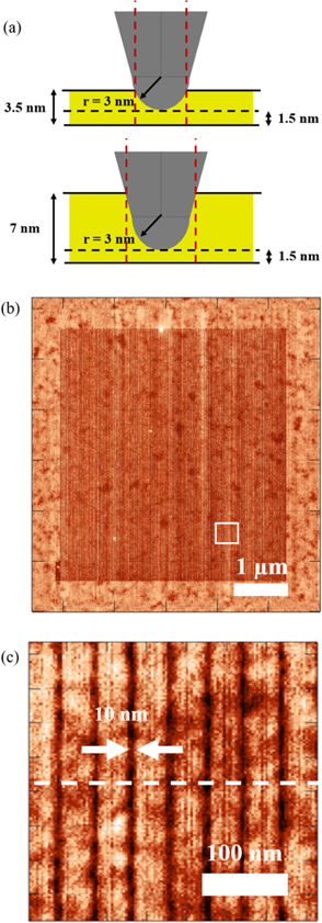
Figure 2. t-SPL patterns. (a) A scheme of the t-SPL tip geometry. The nominal tip radius is 3 nm. The minimum achievable lateral resolution for two different writing depths, 2 and 5.5 nm, is indicated by the dashed red lines. (b) Patterns written in PPA. Overall pattern with slight onset of a dewetting effect of PPA on brush. Z-range is 5 nm. (c) Highly uniform pattern with 10 nm lines at 46.8 nm pitch in a close-up of the area indicated by the white box in (b). Z-range is 5 nm.
Download figure:
Standard image High-resolution imageResults of t-SPL patterning of a 3.5 nm thick PPA layer are shown in figures 2(b) and (c). The patterning step was done at a contact force of 40 nN. The pattern lines were written parallel to the fast scan direction. To write a line, the tip temperature is set to 680 °C for a single scan line. The t-SPL contact-mode image (see figure 2(b)) shows a patterned area of 25 μm2 that has been written with an average tip velocity of 16.1 μm s−1. The total time required for patterning and imaging was 5 min. A pattern with a resolution of 10 nm line width is achieved. This remarkable resolution was obtained by writing shallow patterns of only 2 nm depth, taking advantage of the extremely high resolution of t-SPL for patterning. The pattern pitch is 46.8 nm, which is equal to 2L0, where L0 is the pitch of the block copolymer. In consequence, the multiplication factor η is 2, where η is defined as the ratio of the period of the guiding pattern period to the pitch of the block copolymer. As the patterns are shallower than the PPA film thickness, the polymer brush is not unveiled. The absence of piled-up material on the borders of the written lines proves that the PPA film has indeed been removed by evaporation and not by mechanical force. This observation leads to the conclusion that a tip temperature of 680 °C is sufficiently high for the patterning process.
Fine-tuning of the plasma exposure process is crucial for achieving an optimal chemical guiding pattern. Moreover, the process conditions have to be such that the residual PPA layer in the patterned lines can be removed without removing the PPA layer in the non-patterned areas and without removing the brush layer. This means that during the oxygen-plasma exposure the remaining 1.5 nm PPA layer in the patterned area has to be removed accurately, whereas the 3.5 nm thick pristine PPA layer in the non-patterned area must not be etched away entirely to make sure that the chemical modification of the brush takes place exclusively in the patterned area. Figures 3(a) and (b) compare the patterns before and after oxygen-plasma activation. The area selected for the analysis corresponds to the edge of the patterned area, so that we can compare the change in pattern height with respect to the unpatterned area. After the removal of the residual PPA, the pattern shows a homogeneous and regular line/space pattern (see figure 3(b)). Because of the brush annealing step, the neutral PS-r-PMMA brush layer is grafted onto the silicon surface so that the cyclohexanone dipping step to remove the remaining PPA does not affect the integrity of the brush layer. Interestingly, the previously patterned and oxygen-plasma-exposed areas appear slightly elevated in height with respect to the pristine brush layer. The difference in height is about 1.8 nm.

Figure 3. Documentation of workflow by the mean of AFM images. (a) AFM height image after t-SPL patterning. (b) AFM height image after residual PPA removal, showing the chemical guiding stripes on the polymer brush. (c) AFM height image of aligned block copolymer on guiding pattern depicted in (b). (d) AFM phase image of the same area as depicted in (c). (e) AFM height image after removing the PMMA block by the mean of oxygen plasma. (f) Comparative study of profiles (top to bottom) along the dashed black lines indicated in (a), (b) and (e), respectively. The patterned lines in (1) are recessed, whereas after oxygen-plasma exposure, they are elevated (2). A density multiplication takes place from (2) to (3).
Download figure:
Standard image High-resolution imageFigure 3(c) shows an AFM height image of the resulting block copolymer pattern immediately after self-assembly. As it is difficult to visualize the block copolymer pattern in AFM from the topography, we also present an AFM phase image in figure 3(d). AFM phase imaging helps us to acquire a higher contrast image of the phase separated block copolymer despite the flat sample topography. To enhance the surface contrast of the block copolymer AFM image, a brief oxygen plasma treatment of 5 s at 100 W applied. This leads to a topography contrast between the two blocks because the etch rate of PMMA is larger than that of PS [30, 31] so that the recessed areas correspond to PMMA blocks. The result of this process step is depicted in figure 3(e). The AFM images presented in figures 3(a), (b) and (e) have the same x- and y-scale so that they are directly comparable and the concept of the multiplication factor η becomes evident: the self-assembled pattern is clearly denser than the line pattern fabricated with t-SPL. This is illustrated in the profiles extracted from figures 3(a), (b) and (e) along the dashed lines indicated in figure 3(f). The pattern density multiplication can also be observed by performing the FFT of figures 3(b) and (d) (see figure S5 in the supplemental information)
The SEM images presented in figures 4(a) and (b) contribute to a better understanding of the morphology of the self-assembled structures. Figure 4(a) shows the same DSA pattern as figure 3(e). It exhibits a large-area defect-free DSA. As explained by Wang et al [7], a notable part of the structure in PS-b-PMMA structures with such small domain sizes still consists of a diffuse interface, where the structure is neither pure PS nor pure PMMA. This could explain the relatively large line-edge roughness of the structures, which is even larger after removal of the PMMA block [32]. The absence of defects proves that commensurable guiding patterns can be fabricated with t-SPL. As shown by coarse-grained many-body simulations of self-assembly, BCP may form a wetting layer above wide guiding stripes [33], depending on the strength of the affinity between the modified brush and the blocks. This would lead to a U-shaped configuration of the BCP, in which the structure in top view appears to self-assemble into vertical lamellae, although there is a PMMA bottom layer parallel to the guiding stripes. In our patterns, however, we do not observe any difference in height, pointing to the existence of a wetting layer. This indicates that the guiding patterns are commensurable with L0/2 and that the affinity strength of the guiding patterns is suitable.

Figure 4. SEM images of aligned block copolymer. (a) Defect-free aligned block copolymers on micrometre-scale patterned area with both PS and PMMA blocks present. (b) Comparison of patterned area (right) and non-patterned area (left) shows the influence of the chemical guiding patterns on the self-assembly of the block copolymers. At the bottom on the right of the image, the dimensions of the guiding pattern are indicated. SEM images were taken after removal of the PMMA block by oxygen plasma.
Download figure:
Standard image High-resolution imageFigure 4(b) is an image taken at the edge of the patterned area. On the left-hand side of the image, the characteristic fingerprint pattern can be observed. There is no long-range order in the non-patterned area of the sample. In sharp contrast to that, the block copolymer self-assembles in straight vertical lines on the right-hand side of the image. The patterned and the non-patterned areas can be understood as two adjacent grains. In the patterned area, the BCP self-assemble according to the guiding pattern whereas the adjacent grains nucleate and self-assemble randomly. The transition zone from one area to the other is narrow, and a large number of defects are generated at the interface. The interface can also be referred to as grain boundary. A high density of defects in close vicinity of the grain boundary indicates a large grain boundary energy and thus a large guiding pattern strength. The energy penalty of one defect is in the range of 200 kBT [34].
4. Discussion
Let us now focus on the analysis of the chemical guiding patters. First, we compare the dimensions of the t-SPL pattern with those of the pattern that is subsequently transferred to the brush layer. A single line profile of the pattern shown in figure 3(a) is depicted in the top panel of figure 3(f). The reason why the exposed lines are elevated in height is discussed below. The average line width measured at half minimum is  with a standard deviation
  The full width at half maximum (FWHM) of the lines transferred to the brush layer (see second profile in figure 3(d)) is
  nm, with a standard deviation
  This profile is part of the profile indicated by the dashed line in figure 3(b). Assuming that the nominal tip radius of the imaging probe is 7 nm and the average line height is 1.8 nm, the line width is overestimated by 8.4 nm (tip convolution effect). This implies that the actual FWHM linewidth is
  which means that the plasma activation step causes almost no widening of the structures. Hence the guiding pattern corresponds to 0.52 L0, which is close to the optimal value. Theoretical considerations reveal that (as a function of the guiding pattern strength) the optimal guiding pattern width is slightly below 0.5 L0 to minimize the energy penalty induced by the curvature of the interface between the two blocks [33].
Now we discuss the effect that leads to the swelling of oxygen-plasma-exposed lines in the brush layer. Figure 3(b) shows an AFM height image of a pattern at step 5 that has been exposed to oxygen plasma for 8 s. From this image, we conclude that there is an effect that leads to the swelling of the brush layer after short exposure times, but before the material-removal process begins. The etch rate of PPA was estimated to be 44 nm min−1. Taking into consideration that the device needs about 2.5 s to ignite a plasma, the actual exposure time is reduced to 5.5 s. If we also take into consideration that it takes approximately 2 s to etch through the 1.5 nm of remaining PPA film, the effective exposure time of the film to the plasma is 3.5 s. The swelling effect can be explained by the addition of unspecific functional groups in the exposed areas [35]. One of the characteristics of these functionalized layers is the relatively large ratio of polar hydroxyl groups. The ratio of oxygen on the uppermost polymer layer has been reported to increase and exhibit up to 18–24 oxygen atoms per 100 carbon atoms in the first 2 s of plasma exposure [36]. Polar oxygen-containing groups may be the reason for both the functionalization of the brush and the observed swelling. The existence of polar groups on the surface can explain the attractiveness of these areas to PMMA [19] because methyl methacrylate (MMA) monomers are slightly more polar than styrene monomers.
Extending the effective exposure time by 2 s leads to a pattern in which the exposed lines are on a lower height level than the pristine brush layer, indicating a partial etching of the brush (figure 5(a)). The single line profile depicted in figure 5(b) shows the recess of the exposed areas. We conclude that after the initial formation of functionalized groups, a degradation process of the polymeric films starts once the surface is saturated with oxygen-containing by-products. Particularly, the aromatic ring of polystyrene suffers from degradation because of its large cross section [35]. Previous work suggests that polystyrene loses its aromatic rings relatively fast because it is attached to the rest of the monomer only through a single carbon–carbon bond. This mechanism initiates a crosslinking that leads to the formation of carbon–carbon double bonds [36]. The partial etching of the brush could thus be explained by the removal of aromatic rings from styrene species, which renders the surface chemically less similar to PS, and this in turn favours the wetting of PMMA even more.

Figure 5. The nature of patterned lines after oxygen-plasma activation. (a) AFM height image of an overexposed pattern. (b) Height profile averaged over the box indicated by the dashed white line in (a) shows that the lines in the overexposed pattern are recessed with respect to the pristine brush layer. (c) Behaviour of block copolymers on an over-etched pattern. The morphology changes from vertical to horizontal lamellae.
Download figure:
Standard image High-resolution image
The resulting behaviour of the deposited block copolymer on this pattern is shown in figure 5(c). Increasing the oxygen-plasma exposure time consequently leads to a change of the self-assembly morphology from vertical lamellae to horizontal lamellae. The height of the vertically oriented area increases because vertical lamella BCP can only self-assemble in film thicknesses d with  and
and  As the block copolymer film thickness initially deposited is slightly below the material's natural pitch,
  the difference in height originates in this effect. Furthermore, it is expected that the increased etching time enlarges the width of the functionalized area.
Extrapolating the results of David et al [13] on the use of transferred block copolymer patterns as anti-reflective coating varying the pattern pitch, we expect broad-band anti-reflection properties with a reflectivity dip in the DUV range for 23.4 nm pitch patterns.
5. Conclusions
We have demonstrated the DSA of BCP with very small domain sizes in a chemoepitaxy process using t-SPL as lithography method for creating the guiding patterns. We have shown that it is possible to fabricate dense patterns for aligning the self-assembled block copolymer in the range of 10 nm half-pitch. This result is possible thanks to the inherent absence of proximity effects in t-SPL.
We have demonstrated the fabrication of 10 nm wide chemical guiding patterns using a merely 3.5 nm thick resist mask. For the chemical functionalization of the brush, we have investigated a demanding, but reproducible etching/brush activation process that fulfils all requirements. We have observed the swelling of the activated PS-r-PMMA brush layer when exposed to oxygen plasma for few seconds, which is attributed to the attachment of polar functional groups. Longer exposure times lead to the removal and cracking of aromatic rings and a widening of the exposed areas.
We conclude that brush layer functionalization is exclusively due to the oxygen-plasma activation. We have also shown that we can tailor the strength of the guiding pattern by varying the oxygen-plasma exposure time.
Based on the results presented in this paper, we consider t-SPL to be a viable alternative to EBL for studies that require both high resolution and dense patterns. The process represents a good option for nanofabrication as an alternative to synchrotron radiation or expensive DUV immersion lithography, and it is compatible with the methods commonly used in DSA.
Acknowledgments
This project is partially funded by the EU projects SNM (grant agreement no. 318804) and NFFA (grant agreement no. 654360), and by the Spanish NANOINTEGRA (TEC2015-69864-R). We would like to acknowledge Christophe Navarro and Celia Nicolet from Arkema for supplying some of the polymers used in this work. We would also like to thank Charlotte Bolliger for proofreading the manuscript.