

Abstract
Negative transconductance (NTC) refers to the phenomenon of the N-shape transfer characteristic appearing with a current peak and valley. It has been extensively studied in the past few decades due to its applications in logic and memory devices. Here, we observe unique antibipolar transfer characteristics and NTC behavior in multi-layer 2,6-diphenyl anthracene organic thin-film transistors grown on h-BN, which is due to the vertical potential barrier between the charge accumulation region near the substrate and the neutral bulk region under the contacts. The applied extrinsic electric field could effectively modulate the barrier height, resulting in a competition for charge carrier transport between lateral and vertical directions. Based on the NTC and antibipolar properties, a frequency doubler has been fabricated on a single transistor, which provides a new building block for organic logic circuits.
Export citation and abstract BibTeX RIS
1. Introduction
The multi-terminal devices based on NTC behavior have been heavily studied due to their potential applications in future electronic circuits, such as high-speed switching devices, high-frequency oscillators and memories [1–5]. Most of the reported NTC devices so far were inorganic semiconductor materials, including III–V semiconductors, Si-based materials and two-dimensional atomic crystals [6–10]. However, the counterparts of organic semiconductors were rarely reported due to the poor film quality and low charge carrier mobility. Recently, various organic film growth technologies that can precisely control the thin film thickness and morphology have been developed, such as self-assembly guided strategy [11, 12], alignment of crystalline domains [13, 14] and vapor van der Waals epitaxy [15–17]. The ultra-thin single crystal organic film can be extended to millimeter scale [14, 15, 18]. Coupling with device optimizations, the resulting few-layer molecular crystals have shown outstanding electrical and photo-responsive properties [19–23], and have gained more and more attentions. For instance, several kinds of organic single crystals, such as C8-BTBT, rubrene and 2,6-diphenyl anthracene (DPA), have exhibited the band-like transport behavior with mobility over 30 cm2V−1s−1 [24–26] and photo-responsibility up to 105 A W−1 [20]. Nevertheless, most of studies on organic thin-film transistors (OTFTs) were focused on the electron lateral intralayer transport and how to optimize the contact. The vertical interlayer transport inside organic single crystals has rarely been reported, in which it will afford us a lot of opportunities to explore the new physics in OTFTs.
Here, we studied the interlayer and intralayer charge transport properties of high-quality multi-layer DPA OTFTs grown on h-BN. Antibipolar and NTC behavior were repeatedly observed due to the gate-induced vertical potential barrier change between the charge accumulation region near the substrate and the neutral bulk region inside the DPA thin film under the contact metal, different from the conventional quantum mechanical tunneling and mobility degradation. We systematically investigated the origin of the antibipolar and NTC through variable temperature and bias voltage measurements. Based on the observed NTC phenomenon, we fabricated a frequency doubler on a single OTFT. Our work simplified the structure of the logic device and expanded the application scope of OTFTs.
2. Experiment
2.1. Growth of DPA single crystal film
A DPA few-layer single crystal was grown on h-BN substrate by two-step van der Waals epitaxy in a home-built tube furnace under a high vacuum of ∼1 × 10⁻⁵ torr, similar to our previous reports [16]. Firstly, we placed the mechanically exfoliated h-BN on SiO2/Si substrate and the DPA source power in the center of the heating zone and its upstream 5 cm, respectively. We then kept the heat temperature up to 140 °C for 30 min. After the center of the heating zone cooled down to room temperature, we moved the DPA source powder and the h-BN sample to the center of the heating zone and its downstream 13 cm in sequence. Next, we heated the source up to 135 °C for about 5 min, and then cooled it to 70 °C in 2.5 h.
2.2. Characterization
We carefully characterized the epitaxial DPA single crystal film by optical microscope, atomic force microscopy (AFM) and the cross-polarized optical micrographs. We used AFM performed by Asylum Cypher to characterize the DPA film surface morphology and thickness grown onto h-BN substrate. The cross-polarized optical reflection micrographs were performed by the ScanPro spectro-microscope under the 533 nm laser.
2.3. Device fabrication and measurement
We employed the electrode-transfer technique to fabricate two-terminal and four-terminal devices with Au contact. The thickness of the Au electrodes was 100 nm pre-fabricated by the electron beam lithography process. The details of the transfer process were described in [16] and [17]. All electrical measurements were carried out by a Keithley 4200 semiconductor parameter analyzer in a closed-cycle cryogenic probe station with a base pressure of 10−5 torr.
3. Result and discussion
We first focus on the van der Waals epitaxial growth of single crystal DPA films on exfoliated h-BN substrate, where the atomical flatness and free dangling bonds on the h-BN surface are crucial to deposit the high-quality single crystal thin film (figure 1(b)). Many molecular clusters were found on the surface of h-BN during the first step growth, which would be served as the seed layer for growing the multi-layer single crystal during the second step (figure 1(c); figure S1 is available online at stacks.iop.org/NANO/30/02LT01/mmedia; see experiment section for detailed information about the two-step growth). From figure 1(c), we found that the DPA crystal film preferentially grew on h-BN, in a layer-by-layer growth fashion with atomic smoothness. The average thickness of each molecular layer is 1.89 nm, which is close to the length of DPA (1.777 nm; figure 1(a)), indicating a perpendicular packing on the substrate, which is consistent with previously reported results [27]. Cross-polarized optical micrographs showed that the brightness of the DPA film changed uniformly with a twofold symmetry, as expected for high-quality single crystal (figures 1(d)–(f)).
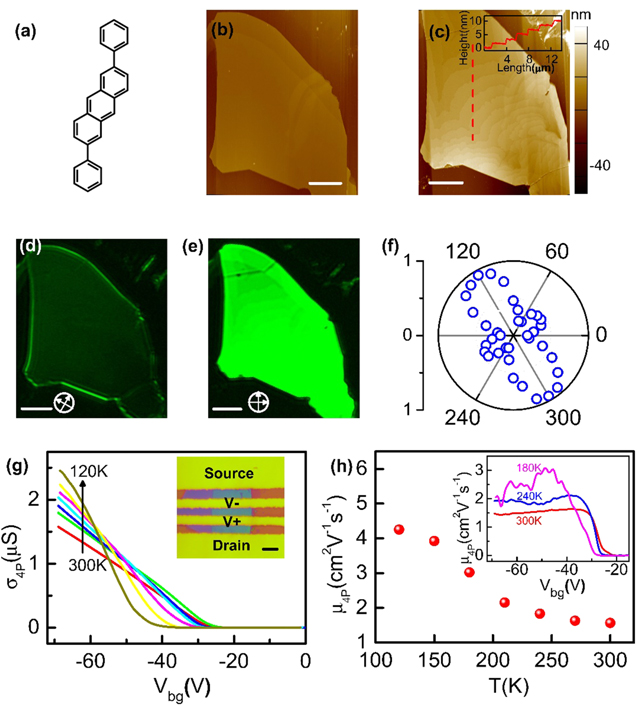
Figure 1. Epitaxial growth of DPA film and basic electrical characterization. (a) Cartoon illustration of the molecular structure of DPA. (b), (c) AFM images of before and after growth of DPA crystals on h-BN, respectively. The inset in (c) is the line profile of DPA film as marked by the red line in (c). (d), (e) Cross-polarized optical micrographs of the sample in (b). (f) Normalized intensity of the DPA crystal under cross-polarized optical microscope as a function of rotation angle. The scale bar in (b)–(e) is 5 μm. (g) Four-terminal conductance in a DPA device plotted as a function of the gate voltage at various temperatures under Vds = −2 V. Inset: The optical microscopic image of the device based on 12.5 nm DPA single crystal film in our measurement. The source (S), drain (D), and voltage probes (V−, V+) are marked. Scale bar: 4 μm. (h) Intrinsic mobility as a function of temperature at Vbg = −50 V. The inset showed the extracted intrinsic mobility as a function of Vbg at different temperatures.
Download figure:
Standard image High-resolution imageNext, we focus on the electrical transport properties of multi-layer DPA transistors, including four-terminal and two-terminal structures (figure S2). Because of the mismatch between the highest occupied molecular orbital (HOMO) energy level of DPA (5.6 eV) and the work function of gold (5.1 eV), a relatively large contact resistance is expected at low bias voltage. To eliminate the influence of the contact resistance and investigate the intrinsic transport properties of DPA single crystal, a four-terminal structure (inset of figure 1(g)) is used in our measurement. The channel conductance  the intrinsic mobility
  and the contact resistance
  could be extracted [28], where
  is the current passing through the channel,
  is the voltage drop between the two probes in the middle separated by D, L is the channel length, W is the channel width,
  is gate capacitance and
  is the back gate voltage applied in the devices. Figure 1(g) shows the temperature-dependent channel conductance as a function of the gate voltage of a four-terminal DPA transistor. The DPA single crystal exhibits clear band-like transport until ∼120 K, shown by the increase of
  and mobility with the cooling. The mobility at Vbg = −50 V increases almost monotonically from ∼1.6 to 4.3 cm2V−1s−1 with temperature decreasing from 300 to 120 K (figure 1(h)). Figure S3 shows the temperature-dependent electrical transport results of another four-terminal DPA transistor with the same qualitative behavior.
Figure 2(a) displays the typical Ids-Vbg transfer characteristics at various temperatures for a two-terminal device with DPA thickness of 18.6 nm (∼10 layers). At room temperature, the device exhibits a standard p-type transport character (figure 2(a), red solid line), consistent with the previous work [26, 27]. Notably, with the temperature decreasing, Ids tends to saturate at large Vbg (e.g., at 170 K), and changes to non-monotonic behavior as a function of Vbg (T < 150 K), showing an interesting antibipolar transfer characteristic and NTC behavior. Such behavior has been reported in multi-layer MoS2 transistors [10], but has never been observed in organic systems to the best of our knowledge. Figure 2(b) shows the Ids-Vds output characteristic at 90 K, where the NTC behavior could be clearly observed at low Vds and persist up to −1.2 V. To further demonstrate the effect of Vds, we plot the Ids-Vbg curves under various Vds from −0.5 V to −1.5 V at 90 K (figure 2(c)). With increasing Vds, the NTC behavior weakens and eventually disappears, and the device restores to a normal p-type OTFT. We note that NTC was observed in all of multi-layer devices and showed significant thickness-dependence as its thickness was over 8.5 nm, but in the thinner DPA devices, typical p-type transistor behavior is observed without NTC (figures S4–S6).
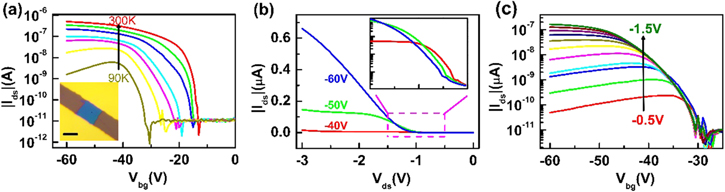
Figure 2. Negative transconductance at low temperature in a two-terminal DPA transistor. (a) Ids-Vbg characteristics (Vds = −1 V) at different temperatures of a typical multi-layer DPA device. The inset is the optical microscopic image of the device. Scale bar: 5 μm. (b) Ids-Vds characteristic under T = 90 K at Vbg = −40 V (red), −50 V (green) and −60 V (blue). The inset shows a detail of the Vds interval where the negative transconductance appears. (c) Ids -Vbg characteristics of the device at T = 90 K under different Vds from −0.5 V to −1.5 V with −0.1 V step.
Download figure:
Standard image High-resolution imageTo further explore the origin of the NTC in multi-layer DPA devices, we have quantitatively analyzed the effective potential barrier of the device based on the variable temperature data. The current across a Schottky contact into a 2D channel can be described by 2D thermionic emission [29, 30],  where the q is the electronic charge,
  is the effective potential barrier height,
  is the Boltzmann constant and
  is the temperature. We extracted the effective potential barrier by linear fitting of the Arrhenius plot at different Vbg (figure 3(a)). The barrier height as a function of Vbg was plotted as shown in figure 3(b). The barrier first decreases and then slowly increases as the Vbg sweeps from −30 V to −60 V, and the position of the minimum
  (Vpeak) corresponds to peak conductance in transfer characteristics. Counterintuitively, we did not observe this variation trend of barrier and NTC in thinner DPA OTFTs. Therefore, we speculated that the change of potential barrier is the main factor leading to the NTC phenomenon. In order to explain the NTC mechanisms, we draw the band diagram under various gate voltage conditions in thicker DPA, as shown in figure 3(d). Here, the barrier includes (I) the Schottky barrier at contact interface and (II) the vertical potential barrier between the charge accumulation region near the substrate and the neutral bulk region under the contacts inside the DPA organic thin film. These two barriers can be effectively tuned by the gate electrostatic coupling effect and source-drain bias. Under the gate voltage being smaller than the threshold voltage, the device is in the off-state. When increasing the gate voltage at the range of Vth ∼ Vpeak, the Schottky barrier dominated the electrons injection and the drain current monotonically increased. With continually increasing gate voltage, the Fermi level of the charge accumulation layer of DPA film near the substrate further shifts down the HOMO and that of the neutral bulk region remaining unchanged owing to the screening effect. Then, the vertical potential barrier height (
 ) was enlarged. This larger vertical barrier reduced the electron transport from charge accumulation layer to neutral bulk region, thus resulting in an n-type behavior. So, the n-type vertical interlayer transport in series with p-type intralayer transport is the main reason for the observed NTC, as shown in figures 2(a) and (c). Meanwhile, due to the drain-induced barrier lowing effect, we did not observe the NTC behavior at large source-drain bias. Furthermore, we carried out four-terminal measurements in the NTC regime. Figure 3(c) shows the total, channel and contact resistance as a function of Vbg. We observe that Rcontact is one order of magnitude larger than Rchannel and presents a non-monotonic change (figure 3(c) inset), while the Rchannel always decreases with increasing gate voltage, consistent with the expected p-type behavior, indicating that the vertical potential barrier dominates the electron transport.

Figure 3. Mechanism of negative transconductance. (a) Arrhenius plot of ln(Ids/T3/2) of the multi-layer device in figure 2 under Vbg = −36 V (red), −42 V (green), −48 V (blue), −54 V (cyan), −60 V (magenta). (b) Derived barrier height as a function of Vbg. At the high gate voltage, the  increases with the gate voltage further increasing, exhibiting an n-type barrier behavior. (c) Vbg dependence of the total resistance, the extracted contact resistance and the DPA channel resistance of the four-terminal device tested in figure 1(g). The inset demonstrates a detail of the Vbg interval where the negative transconductance appears. (d) The device schematics and band alignment of thick multi-layer DPA transistor under different gate voltages, Vbg < Vth (left), Vth < Vbg < Vpeak (middle) and Vbg > Vpeak (right).
Download figure:
Standard image High-resolution imageDue to the unique NTC behavior, the sign of the transconductance could be switched from positive to negative, which provides new opportunities in the field of analog circuits applications. We fabricate a frequency doubler using a single multi-layer DPA OTFT. As displayed in figure 4(a), the DC offset voltage carrying a sinusoidal AC signal is applied as the input signal, with a 50 MΩ resistor connected to the source electrode in the circuit. From the transfer characteristic of the device in the circuit shown in figure 4(b), we could get that the peak-to-valley ratio is about 5.1, which is defined by the ratio of maximum peak current (Ipeak) versus the valley current at the largest gate voltage (Ivalley at Vbg = −70 V,), and Vpeak = −50 V. When Vin < Vpeak, the transconductance is positive and the output voltage increases with increasing of the input AC signal; when Vin > Vpeak, the transconductance is negative and the output voltage decreases as the input AC signal increases. Therefore, a maximum and a minimum value appear simultaneously on one side of Vpeak when Voffset is set to Vpeak, implementing a frequency doubler. We set the Voffset = −50 V and use the sinusoidal AC signal with a frequency of 40 mHz as the input single, shown in the upper panel of figure 4(c), then an 80 mHz AC signal (bottom panel of figure 4(c)) will output from the circuit.

Figure 4. Frequency doubler based on signal DPA transistor. (a) The circuit of the DPA transistor frequency doubling. The circuit employs a signal DPA transistor in series with a resistor (50 MΩ). Bias voltage (Vdd) is 0.8 V and the measurement temperature is 60 K. The offset voltage is a DC voltage, and the signal is an AC sinusoidal voltage. (b) The corresponding transfer characteristic of this multi-layer DPA transistor, demonstrating obvious NTC behavior. At Vbg = −50 V, the channel current (Ids) reaches to a peak. (c) Input AC signal (up) and output (bottom) signal when the offset voltage is −50 V. The frequency of the input signal is 40 mHz, and the output signal is 80 mHz.
Download figure:
Standard image High-resolution image
4. Conclusion
In conclusion, high-quality multi-layer DPA single crystal films have been grown on h-BN substrate, and the OTFTs exhibited obvious band-like transport characteristics down to 120 K. Further, we observed a unique antibipolar and obvious NTC behavior in the multi-layer organic semiconductor transistors, due to a competition for charge carrier transport between lateral and vertical directions. The vertical potential barrier between the charge accumulation region near the substrate and the charge neutral bulk region inside DPA organic thin film under the contact metal, effectively modulated by the applied extrinsic electric field, is the fundamental origin, which was further testified from the temperature and source-drain bias dependence measurement. Based on the NTC and antibipolar phenomena, a frequency doubler had been fabricated using a single organic transistor.
Acknowledgments
The authors acknowledge support from the National Natural Science Foundation of China (Grant Nos. 61734003, 61704073, 61521001, 51725304, 51633006), National Key Basic Research Program of China (Grant Nos. 2013CBA01604 and 2015CB921600) and the Ministry of Science and Technology of China (2017YFA0204503).