

Abstract
We studied optical properties and photocurrent characteristics of PbS nanowires grown by chemical vapor deposition. Distinct bandedge photoluminescence (PL) emission was observed in the mid-infrared spectral range and the quantum confinement effect estimated from the PL peak energy was within 40 meV, consistent with the average diameter of the nanowire (∼70 nm) being significantly larger than the exciton Bohr radius (∼18 nm). We also demonstrated interdigit photo detectors making use of these PbS nanowires suspended between two pre-patterned Ti electrodes, where Ti also acted as metal catalyst for the nanowire growth. The threshold wavelength of the photocurrent was found to be ∼3 μm at room temperature.
Export citation and abstract BibTeX RIS
1. Introduction
Lead sulfide (PbS) nanostructures have attracted much attention for optoelectronic applications such as photo-detectors [1] and photovoltaic devices [2–4]. Among the nanostructures, PbS nanowires grown by chemical vapor deposition (CVD) method demonstrated very high electron mobility up to 660 cm2 V−1 s–1 at room temperature [5], indicating that their crystal quality is high and that the surface carrier trapping, or scattering does not play an important role in PbS nanowires. PbS has a cubic rock salt structure and the nanowires typically grow along [100] direction with CVD method [6]. Bulk PbS has a direct bandgap at 0.41 eV at room temperature and its bandgap shrinks down to ∼0.3 eV (∼4.3 µm) at 10 K [7, 8], making it suitable for mid infrared detectors.
Although impressive results have been already demonstrated from single PbS nanowire devices, they were typically fabricated by expensive and time-consuming method such as electron-beam lithography to define electrodes and it is still quite challenging to obtain device performance on a mass production scale. Additionally, for vertical type detectors [3, 4], transparent top contact electrodes are necessary in order for the incident light to reach PbS. For the application of mid infrared detectors, it is difficult to develop suitable transparent electrodes since most transparent oxide materials typically exhibit strong absorption near mid infrared due to free carrier absorption.
It is well known that the bandgap of PbS nanostructures increases by the quantum confinement effect when the physical dimension of the nanostructures is less than their exciton Bohr radius of 18 nm, which is well demonstrated from the size dependent bandgap of PbS nanocrystals, or quantum dots [9]. On the other hand, it is rare to find literatures regarding the photoluminescence (PL) study in the mid-infrared spectral range for PbS with relatively large physical dimensions [7, 10]. Detailed studies on the PL characteristics of CVD grown PbS nanowires, including the origin of the emissions and the temperature dependent intensities and line-widths, have not been discussed previously. PL studies provide useful information on non-radiative recombinations and surface trapping effects, which could be crucial for the performance of optoelectronic applications.
In this paper, we discuss PL properties of PbS nanowires grown by CVD whose average diameter is ∼70 nm, larger than the exciton Bohr radius. PL spectra were taken in the temperature range of 10–300 K with a Fourier transformed infrared (FTIR) set-up, allowing full spectral measurements. We also report PbS nanowire bridge photodetectors for the first time. The photodetectors were fabricated making use of the PbS nanowires which were suspended between two pre-patterned Ti electrodes, which also act as metal catalyst for the nanowire growth. Since it is easy to obtain long nanowires (>20 μm), the suspended nanowires connect the two separated electrodes whose gap is as large as 20 μm. Also, these detectors do not require top contact electrodes, which could be important for the future development of mid-, or far-infrared detectors.
2. Experimental
PbS nanowires were synthesized via a CVD approach inside a tube furnace. Two precursors, PbCl2 and S powders, were placed at the center of the furnace and initially outside the heating zone, respectively. The growth substrates consist of Ti coated Si wafers with thermal oxide on top. In a standard growth, the substrate is placed 5 cm downstream from the center of the furnace, where the temperature is measured to be around 600 °C. The quartz tube was first evacuated to a base pressure of 15 mTorr, and then filled with N2 to atmospheric pressure. The N2 flow was maintained at 150 sccm while the furnace center temperature was ramped to 630 °C. Once the peak temperature is reached, the nanowire growth is triggered by transferring S into the heating zone of 450 °C. The growth duration varies from 30 min to 1 h. Subsequently, the temperature of the furnace is naturally cooled down to room temperature. The as-grown samples appear black in color.
PL spectra were measured using a Bruker Vertex 80 V Fourier transform spectrometer, equipped with a KBr beam-splitter and diamond/CsI windows, the excitation wavelength being 532 nm. For temperature dependent measurements, samples were mounted inside a vibration-free closed-cycle He optical cryostat immersed in the FTIR set-up, prohibiting moisture/gas absorption in the air. Optical windows of the cryostat were made of ZnSe to reduce the absorption in the mid-ir range.
For the fabrication of photo detector devices, PbS nanowires were grown on top of interdigit Ti (thickness ∼50 nm) electrodes, which were pre-patterned on SiO2/Si substrates by photolithography. The gap between the interdigit electrodes was varied between 5 and 20 μm, the metal stripe width being kept the same as the gap width. The length of the electrodes was 160 μm. The I–V characteristics were measured by using an ammeter with a sensitivity of pA and the photocurrent characteristics were obtained using the 514.5 nm laser beam from an Ar+ laser, the excitation power being 7 mW. The wavelength dependent photocurrent is measured using a tunable laser (NKT SuperK), with wavelength varying from 600 to 1700 nm as well as using the FTIR set-up. All measurements were done at room temperature if not specified.
3. Results and discussion
Figure 1(a) shows the PL spectra of PbS nanowires grown by CVD method using Ti catalysts at various temperatures T. The PL peak blue-shifts with increasing temperature, as expected for PbS [8], and the PL intensity decreases with increasing temperatures due to the increasing contribution of non-radiative recombinations at higher temperatures. The integrated PL intensity is shown in figure 1(b) as a function of temperature. The ratio of the integrated PL intensity from 10 to 300 K for the nanowires is only about 1/3, compared to 1/20 [7] for nanocubes grown by hydrothermal method, indicating that the role of non-radiative recombination centers is significantly less in CVD-grown nanowires probably due to the reduced structural and point defects. This could be also associated with the reduced surface recombination in the nanowires associated with their unintentional surface passivation.
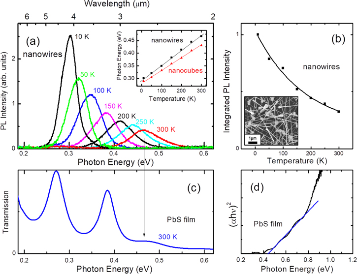
Figure 1. (a) PL spectra of PbS nanowires at various temperatures. In the inset, we show the PL peak energies as a function of temperature for PbS nanowires (■) and sub-micron size PbS nanocubes (▲). (b) Integrated PL intensity as a function of temperature for the nanowires. Inset shows an SEM image of the nanowires. (c) Transmission spectrum of a PbS film at 300 K, demonstrating the absorption edge. The oscillations below the bandgap are due to interference fringes. (d) A fitting curve used for the bandgap estimation of PbS film.
Download figure:
Standard image High-resolution imageThe blue-shift of the bandgap Eo in PbS with increasing temperatures is known to be associated with the abnormal negative value of  T, where P is the pressure, leading to the increase of the bandgap by the lattice thermal expansion [8]. In the inset of figure 1(a), we show the change of the PL peak energy (■) as a function of temperature T. PL peak energies of the nanowires are very close to, but slightly higher than the reported values for bulk PbS. As we will discuss below, the quantum confinement effect from these nanowires is within 40 meV since the average diameter of our nanowires being ∼70 nm, significantly larger than the exciton Bohr radius of 18 nm. Due to the large variation of the nanowire diameters, some nanowires are as thin as 25–30 nm, closer to the exciton Bohr radius. The full-width at half maximum of the PL peak is as large as 40 meV at 10 K, which is twice of that for the sub-micron size nanocubes [7]. The PL peak broadening is probably due to the variation of the confinement effect associated with the diameter variation. In the inset, we also showed the PL peak energies (▲) of the nanocubes, for comparison. From the temperature dependence of the PL peak energy, we obtain a slope dE/dT = 5.7 × 10⁻⁴ eV K−1, reasonably close to 4.9 × 10⁻⁴ eV K−1, the value we previously reported for sub-micron size nanocubes.
We changed the Pb and S ratio for the growth of the nanowires and studied the change of the PL spectra with doping. It has been shown earlier that the carrier type of PbS nanowires depends on the PbCl2/S precursor mass ratio [5]. A Pb rich growth condition leads to n-type nanowires, while a S rich condition generates p-type nanowires. However, it was found that the PL peak energies do not exhibit any systematic variation with doping conditions, indicating that the PL emission probably originates from the bandedge emission due to the recombination between the electrons in the conduction band minimum and the holes in the valence band maximum, rather than from acceptor or donor related recombinations such as donor-acceptor pairs. The PL peak energy was not changed by the excitation density (not shown), also supporting this conclusion. The exciton binding energy of PbS is less than 4 meV [11], which corresponds to the value of kT at T ∼ 50 K. For T ≤ 50 K, excitonic transition could be important, whereas bandedge emission becomes dominant for T > 50 K. Since the exciton binding energy is significantly less than the PL line-width, the PL peak energy can be considered to be the bandgap energy of the PbS nanowires for all temperature ranges.
While transmission spectra could not be obtained from these CVD-grown nanowires due to the metal catalyst used for their growth, which blocks most of the light, we show the room-temperature transmission spectrum of 0.2 μm thick PbS film deposited by thermal evaporation method in figure 1(c). The film was deposited on a Si substrate at 250 °C. In the transmission spectrum, oscillations are observed for photon energy below the bandgap due to the interference effect by the multiple reflections between the film and the Si substrate, indicating the smooth surface of the film. The oscillation suddenly disappears and the transmission drops to almost zero above the absorption edge. In figure 1(d), we show a plot of (αhν)2 versus photon energy hν, which is typically used for bandgap estimation in direct bandgap semiconductors. Here, α is the absorption coefficient. Although it is difficult to obtain a good linear fit, the bandgap of the film appears very close to the PL peak energy of the nanowires, consistent with almost negligible quantum confinement. We note here that we were able to detect PL emission at ∼0.3 eV at 10 K from the film, but it was extremely weak and noisy even at 10 K (not shown).
In order to fabricate photo detectors, the nanowires were grown on top of interdigit Ti electrodes pre-patterned by photolithography on SiO2/Si substrates. Figure 2(a) shows an SEM image of an interdigit device, where the nanowires grow only on the metal pattern. As seen in the SEM image of figure 2(b), the nanowires grow on the surface of PbS micro crystal seeds, which grow by direct deposition from vapor (i.e., vapor–solid mechanism). This is similar to the observations by Ge et al [12]. The authors found that the PbS nanowires grow perpendicular to the cubic faces (or along x, y, and z directions), forming orthogonal networks, the growth direction being along 〈100〉. Figure 2(e) shows a low-resolution Transmission electron microscope (TEM) image and a Selected area electron diffraction (SAED) pattern, confirming the growth direction along 〈100〉. A high resolution TEM image in figure 2(f) demonstrates the single crystalline nature and the inter-plane distance along 〈100〉 is found to be 2.96 Å, which is the half of the lattice constant (a = 5.93 Å), as expected. While the exact growth mechanism of the nanowires is out of the scope of this paper, we would like to mention that Ti influences the formation of the PbS micro crystal seeds, since both the crystals and the nanowires are mostly found only on the Ti deposited area. (Please see additional SEM images of interdigit devices, in supplementary figure S1, which are available online at stacks.iop.org/NANO/28/475706/mmedia.)
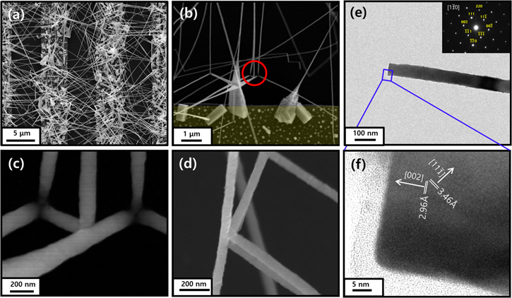
Figure 2. (a) An SEM image of an interdigit device using PbS nanowires. The gap and the metal stripe widths are 5 μm for this device. (b) An SEM image in a lower nanowire density area, in order to show that the nanowires grow on the surface of the micro crystals. As marked by the red circle, when the nanowires touch the SiO2 surface, they continue to re-grow in orthogonal directions. (c) An enlarged SEM image of the red circle area. (d) An SEM image that demonstrates that some nanowires merge during the growth, possibly by the static force, or by the Van der Waals force between the nanowires. (e) A low resolution TEM image of a nanowire with an SAED pattern. (f) A high resolution TEM image of the nanowire.
Download figure:
Standard image High-resolution imageAs can be seen in figures 2 and S1, there are areas on the Ti electrodes free of PbS nanowires. This could be caused by two possible mechanisms. One is nucleation exclusion zone: the zones in the vicinity of nuclei have a reduced and even zero nucleation rate because of the consumption of the diffusing adatoms. The other is partial oxidation of Ti, which can potentially lower its catalytic efficiency and even create a contact barrier in the final device. We have tried to minimize oxidation by storing Ti covered substrate in a nitrogen glovebox and by achieving low base pressure in the reaction quartz tube. We did not observe any obvious change such as in color or morphology in the Ti film and Ti remained conductive after nanowire growth. However, this does not exclude the possibility of slight surface oxidation of Ti.
It was found that some PbS nanowires merge during the growth, possibly by the static force, or by the Van der Waals force between the nanowires (see figure 2(d)). As seen in figure 2(b), PbS nanowires sometimes touch the SiO2 surface and continue to re-grow in orthogonal directions. Figure 2(c) shows the enlarged image of this area.
The inset in the upper right corner of figure 3(a) shows the I–V characteristics of an interdigit device under the exposure of the light (red) as well as in the dark condition (black), measured with the 514.5 nm laser beam from an Ar+ laser, powder density being ∼9 W cm−2. Both the electrode gap and the metal stripe width were 10 μm and the length of each stripe was 160 μm. Total active area of the device was 160 × 600 μm2. The I–V curves are slightly nonlinear as a function of applied bias due to a Schottky contact between PbS and Ti metal. The temporal response of the photocurrent for the interdigit device is shown in figure 3(a) under the applied voltages of 1 and 2 V. The relatively slow photo response indicates the existence of the carrier traps; the rise time corresponds to the carrier filling time and the decay time represent the carrier release time from the traps. In a p-type PbS photoconductive film, an electron trap level is known to be 0.2 eV below the conduction band [13]. Similar trap states may also play a role in the nanowires. The decay time of the photocurrent was found to decrease with increasing applied voltage, while the change is less apparent for the rise time. In figure 3(b) we show the decay of the normalized photocurrent with various voltages.
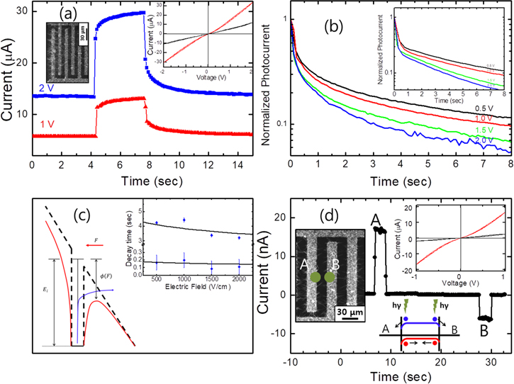
Figure 3. (a) Time trace of the photocurrent from an interdigit device under a bias voltages of 1 and 2 V as the laser was turned on and off. The inset in the upper right shows I–V characteristics of the device under the exposure of the light (red) as well as in the dark condition (black). (b) Normalized photocurrent decay under the bias voltages of 0.5, 1, 1.5, and 2 V, demonstrating the decrease of the decay time with increasing bias. The theoretical fits are shown in the inset. (c) A schematic diagram of the Poole–Frenkel model. In the model, the decrease of the decay time with increasing bias is explained by a decrease of the effective potential barrier of the electron trap. The curves in the inset shows the theoretical decay time as a function of the electric field. (d) Time trace of photovoltaic current due to the Schottky contact between PbS and Ti metal. The inset shows I–V characteristics of the device with and without laser excitation.
Download figure:
Standard image High-resolution imageWe fit the normalized photocurrent decay with two exponential decay components such that 
 and
and  being the carrier release times from two types of traps. From the fit,
  was found to be ∼6.5:2.5, indicating faster decay component is larger than the slower one. A small value of
  represents the persistent photocurrent component, which decreases from 0.07 at 0.5 V to 0.03 at 2 V. The inset in figure 3(b) shows the fitting curves. As seen, the decay time of the photocurrent clearly decreases with increasing bias. The values of
  and
and  from the fits are shown in figure 3(c) as a function of an electric field. Here the strength of the electric field is simply the bias voltage divided by the gap of the electrodes, assuming that the bias voltage is only applied to the body of the nanowire and that the length the suspended nanowires is the gap width of 10 μm.
The decrease of the carrier release time with increasing electric field can be understood as a decrease of the effective potential barrier of the trap. The carrier release time is given by ![${\tau }^{-1}={\sigma }_{n}{N}_{{\rm{c}}}{\nu }_{{\rm{t}}{\rm{h}}}\exp [-({\rm{\Delta }}E)/kT],$](https://content.cld.iop.org/journals/0957-4484/28/47/475706/revision2/nanoaa8fa5ieqn9.gif) where
where  is the capture cross section of the trap,
  is the density of states in conduction band,
  is the thermal velocity of the carriers, and
  is the energy barrier of the trap measured relative to the conduction band edge [14]. Here, the effective potential barrier
  where
where  is the trap level without electric field and
  is the decrease of the potential barrier under an external electric field. Following the Poole–Frenkel mechanism for a charged trap,
  where
where  is the dielectric constant (see figure 3(c)) [15]. Then the carrier release time decreases with increasing E, such that
 ![$\tau ={\tau }_{0}({E}=0)\exp \left[\tfrac{-e\sqrt{eF/\pi {\varepsilon }_{S}\,}}{kT}\,\right].$](https://content.cld.iop.org/journals/0957-4484/28/47/475706/revision2/nanoaa8fa5ieqn19.gif) The solid curves shown in figure 3(c) are obtained using
The solid curves shown in figure 3(c) are obtained using  for
for  At 2 V (corresponding to E = 2 kV cm−1), the decrease of the potential barrier
  and
and  is expected to be
  which reasonably agrees with the experimental data.
Figure 3(d) shows the switching characteristics of the photocurrent at zero bias at the left (A) and right (B) hand sides of the gap for another device (D20) with both the gap and the metal stripe width being 20 μm. Total active area of the device was 160 × 800 μm2. More photocurrent data can be seen in supplementary figure S2 and the SEM image of the whole device is included in the inset of the figure. The positive and negative photocurrents were obtained by shining a focused laser beam at the left and right hand sides of a gap, respectively. Such photovoltaic current is due to the Schottky contact and the response time is very fast with no persistent photocurrent. The I–V characteristic of D20 is shown in the upper right corner of figure 3(d). Using the value of 0.3 eV for the difference of the work function of Ti (4.3 eV) and the Fermi level of p-type PbS (4.6 eV) and the depletion width ∼24 nm, the maximum electric field at the Schottky contact is ∼250 kV cm−1. In case of Poole–Frenkel mechanism, the decrease of the potential barrier  yielding the expected
  value of 0.12 s. which can explain the experimentally observed fast response. It is also possible that the potential barrier of the traps is comparable with, or less than 90 meV.
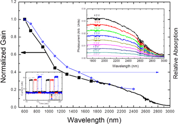
The wavelength dependent photocurrent is measured using a tunable laser (see the botom left inset in figure 4) under a bias voltage of 0.1 V. The gap between the interdigit electrodes was 10 μm. Figure 4 shows the excitation wavelength dependence of the gain (■), which is calculated by (ΔI/e)/(P/hν), where ΔI = Ilight − Idark is the photocurrent. Since the maximum wavelength of the tunable laser was 1700 nm, the photocurrent spectra for a longer wavelength range were obtained using a FTIR setup, which are shown in the upper right inset of figure 4. The decrease of the gain with increasing wavelength closely reflects the decrease of the PbS absorption (○) calculated using absorption coefficients in [16]. We note here that this spectral response is quite different from that of chemically deposited polycrystalline PbS films studied by Blount et al [17], who observed a decrease of the photoconductivity with increasing photon energy. The authors explained their spectral response by the trapping effect. Konstantatos and Sargent pointed out in colloidal quantum dot systems [14] that the surface passivation together with quantum confinement may determine the trap state energy and the photocurrent decay. Further investigation is necessary to identify the trap state energy in PbS nanowires.
Figure 4. Normalized gain of an interdigit device as a function of laser excitation wavelength. The photo response in the infrared range is demonstrated up to 1.7 μm using a tunable laser. The excitation power was 2 mW up to 0.9 μm and 2.5 mW above 1 μm. The bottom left inset shows the time trace of the photocurrent for excitation wavelengths of 0.6, 1.1, and 1.7 μm under a bias voltage of 0.1 V. In the upper right inset, we show the photocurrent spectra in the longer wavelength range at various bias voltages obtained using a FTIR setup. The absorption (○) curve was calculated using the average diameter (70 nm) of nanowires.
Download figure:
Standard image High-resolution image
4. Conclusions
In summary, we discussed the temperature dependent PL properties of PbS nanowires grown by CVD method. The ratio of the integrated PL intensity from 10 to 300 K for the nanowires is only about 1/3, indicating high optical quality of these nanostructures. From the temperature dependence of the PL peak energy, we obtain a slope dE/dT = 5.7 × 10⁻⁴ eV K−1, reasonably close to the reported values, including that for sub-micron size. Optical properties presented in this work is important for developing mid-infra light emitting diodes.
In addition, we demonstrated the photo response up to ∼3 μm by using interdigit devices made of these nanowires grown on top of pre-patterned Ti electrodes, where Ti also acted as metal catalyst for the nanowire growth. It was found that the photocurrent decay contains slow component  which decreases with increasing bias voltage. This is explained by the decrease of the effective energy barrier of the carrier trap under an external electric field. The interdigit type of photo-detectors does not require top contact electrodes, which is especially useful for mid-, or far-infrared detectors.
Acknowledgments
This research was supported by Basic Science Research Program through the National Research Foundation of Korea (NRF) funded by the Ministry of Education (2015-1997-01) and Chungnam National University.